Imaging the Kondo Insulating Gap on SmB6
Abstract
Topological insulators host spin-polarized surface states which robustly span the band gap and hold promise for novel applications. Recent theoretical predictions have suggested that topologically protected surface states may similarly span the hybridization gap in some strongly correlated heavy fermion materials, particularly SmB6. However, the process by which the Sm electrons hybridize with the electrons on the surface of SmB6, and the expected Fermi-level gap in the density of states out of which the predicted topological surface states must arise, have not been directly measured. We use scanning tunneling microscopy to conduct the first atomic resolution spectroscopic study of the cleaved surface of SmB6, and to reveal a robust hybridization gap which universally spans the Fermi level on four distinct surface morphologies despite shifts in the band energy. Using a cotunneling model, we separate the density of states of the hybridized bands from which the predicted topological surface states must be disentangled. On all surfaces we observe residual spectral weight spanning the hybridization gap down to the lowest , which is consistent with a topological surface state.
The classification of solids based on topological invariants has led to the recognition of new electronic phases of matter. The existence of non-trivial topology in band insulators, combined with time reversal or crystal symmetries, gives rise to topologically protected metallic surface states.Fu et al. (2007) Potential applications ranging from spintronics to quantum computing have driven intense research efforts into the surface states of topological band insulators such as Bi- and Sn-based chalcogenides.Ando (2013); Hasan and Moore (2011); Qi and Zhang (2011) Recently, it was suggested that similar topological arguments could apply to the more strongly correlated Kondo insulators.Dzero et al. (2010) In these heavy fermion compounds, itinerant electrons screen the local magnetic moments of the lattice in a process known as the Kondo effect.Coleman (2007) At temperatures below the Kondo coherence temperature () the conduction electrons hybridize with the magnetic moments to open up an energy gap in the density of states (DOS). In a Kondo insulator, the hybridization gap spans the Fermi level , causing a metal to insulator transition upon cooling through . In a topological Kondo insulator (TKI), protected chiral surface states are predicted to span the Kondo hybridization gap.
Recently, there has been tremendous interest in the heavy fermion material SmB6 as a possible TKI.Dzero et al. (2010); Takimoto (2011); Lu et al. (2013) SmB6 undergoes a metal to insulator transition around 50 KMenth et al. (1969); Allen et al. (1979); Cooley et al. (1995) which has been attributed to hybridization between the electrons and conduction band. Below 3 K, a saturation in the resistivityMenth et al. (1969); Cooley et al. (1995) indicates a zero temperature conducting channel which could be explained by the existence of topologically protected surface states.Dzero et al. (2010); Takimoto (2011) This hypothesis has been investigated by a number of recent point contact spectroscopy,Zhang et al. (2013) transport,Kim et al. (2012); Wolgast et al. (2012); Kim et al. (2013); Thomas et al. (2013) quantum oscillation,Li et al. (2013) and angle-resolved photoemission spectroscopy (ARPES)Miyazaki et al. (2012); Xu et al. ; Jiang et al. (2013); Neupane et al. (2013); Frantzeskakis et al. (2013) experiments. The dispersion and orbital chirality of some surface states,Jiang et al. (2013) the half integer Berry phase from Landau levels,Li et al. (2013) and transport response to magnetic impuritiesKim et al. (2013) are strongly suggestive of nontrivial topology in SmB6.
Although evidence is accumulating for topological surface states on SmB6, precise understanding of their properties is presently limited by poor understanding of the hybridization gap within which they emerge. DC transportMenth et al. (1969); Cooley et al. (1995); Flachbart et al. (2001) and optical reflectivityTravaglini and Wachter (1984) studies typically report a gap of 5-10 meV, but both the activation energy fits and the Kramers-Kronig transformations necessary to extract these gap energies may be affected by residual states in the gap.Cooley et al. (1995); Flachbart et al. (2001); Gorshunov et al. (1999) Larger gaps of 19 meV and 36 meV have also been observed by optical transmissivityGorshunov et al. (1999) and Raman spectroscopy,Nyhus et al. (1995) respectively. However, transport and optical techniques cannot determine the gap center with respect to . Angle-resolved photoemission spectroscopy (ARPES) experiments, which measure filled states only, loosely identify the magnitude of the hybridization gap as the binding energy of the sharp band just below , typically 14-20 meV.Miyazaki et al. (2012); Xu et al. ; Jiang et al. (2013); Neupane et al. (2013) However the lack of information on the empty state side makes even the simple question of whether the gap spans the Fermi level elusive.Frantzeskakis et al. (2013)
Planar tunneling and point contact spectroscopy (PTS/PCS) purport to measure the complete DOS, showing the -dependent opening of a gap 14-22 meV.Amsler et al. (1998); Flachbart et al. (2001); Zhang et al. (2013) However, PCS lineshapes in SmB6-SmB6 junctions vary dramatically with junction size,Flachbart et al. (2001) while PTS and PCS heterojunction experiments have shown an asymmetric peak on the positive energy side of the gap,Amsler et al. (1998); Zhang et al. (2013) in contrast to the preponderance of theoretical and experimental evidence for an electron-like conduction band.Lu et al. (2013); Alexandrov et al. (2013); Miyazaki et al. (2012); Xu et al. ; Jiang et al. (2013); Neupane et al. (2013); Frantzeskakis et al. (2013) It remains crucial to access the bare DOS and full hybridization gap.
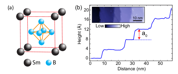
The aforementioned studies on SmB6 have averaged over at least several microns of surface area. Spatial averaging over large regions of SmB6 is problematic because, unlike the first generation of Bi-based topological insulators, which are layered materials with natural cleavage planes, SmB6 is a fully three dimensional material whose cleavage properties are unknown. SmB6 has a CsCl-type cubic crystal structure with alternating Sm2+ ions and B octahedra, shown in Fig. 1a. It is therefore expected that complete Sm2+(001) or B(001) terminations would be polar, resulting in surface band bending. On the other hand, a partial Sm surface may suffer from structural reconstructions as seen by low energy electron diffraction (LEED).Aono et al. (1979); Miyazaki et al. (2012) Although the topologically protected surface states are expected to exist on all surface morphologies, their manifestation may be influenced by the differing electronic environments in which they live. Furthermore, the possible shifts of the hybridization gap and/or coexistence of topologically trivial states on some surfaces may short out the fundamental chiral states of interest for transport devices. It remains crucial to quantify the hybridization gap itself, and to understand its variation with surface morphology. Here we use atomically resolved scanning tunneling microscopy and spectroscopy (STM/STS) to probe variations in differential tunneling conductance () across multiple SmB6 surface morphologies. We demonstrate that vacuum tunneling conductance is dominated by the bare DOS, and shows a robust hybridization gap which universally spans the Fermi level on all surfaces, as well as anomalous in-gap spectral weight.
Results
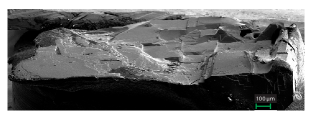
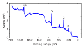
Surface structure. The topographic image in Fig. 1b shows the cleaved surface of SmB6 with atomically flat terraces of typical 10 nm extent. Terraces are separated by steps of height equal to the cubic lattice constant Å, which identifies the cleaved surface as the (001) plane. After the conclusion of the STM experiment, we performed electron back scatter diffraction (EBSD) and x-ray photoelectron spectroscopy (XPS) measurements which confirmed the (001) orientation and showed a B-rich surface,Sup consistent with previous measurements.Aono et al. (1979)
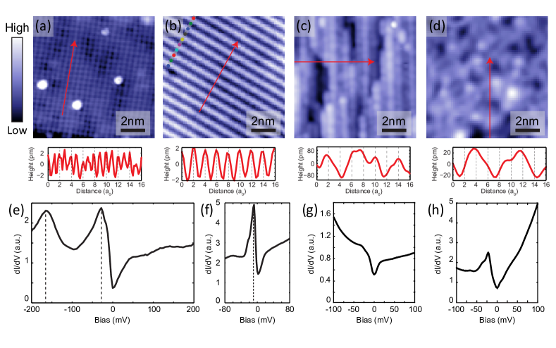
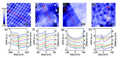
Figure 2 shows higher resolution topographies of the four distinct surface morphologies we observed. Figure 2a shows a rarely observed square lattice which we identify as a complete Sm layer, similar to the complete La layer of (001) cleaved LaB6 previously imaged by STM.Ozcomert and Trenary (1992) Because the Sm atoms have a valence of 2+, this polar surface may be energetically unfavorable,Gao et al. (2010) explaining its typical limitation to small regions approximately 10 nm 10 nm on the cleaved surface. The polar instability of the surface could be resolved by removing half of the Sm atoms from the topmost layer, consistent with the striped surface in Fig. 2b (also shown on the terraces of Fig. 1b). This surface is consistent with LEED observations of a reconstructionMiyazaki et al. (2012) and ARPES observations of band-foldingXu et al. ; Jiang et al. (2013) on the cleaved SmB6 surface. However, we find that the majority of the cleaved surface is disordered and can be classified as filamentary or amorphous, shown in Figs. 2c-d, respectively. Both of these disordered surfaces show corrugations larger than the suspected Sm terminations in Figs. 2a-b. Furthermore, the terrace step heights between these disordered morphologies are non-rational multiples of . We speculate that the commonly observed filament morphology could be a reconstruction of the B6 octahedra, consistent with our XPS measurements showing that the average surface is B-rich.Sup
bands and hybridization gap. Having assigned chemical identities to these surface morphologies, we image their differential tunneling conductance , which is typically proportional to the local DOS.Bardeen (1961) Figs. 2e-h show spatially averaged spectra representative of each of the four surfaces, emphasizing some ubiquitous features, as well as dramatic differences between the morphologies. The dominant features common to all surfaces are the spectral minimum located near the Fermi energy, and the relative prominence of the peak on the filled state side, compared to the empty state side. Both observations are consistent with the bare DOS for a hybridized electron-like conduction band.Figgins and Morr (2010)
To better understand the band hybridization, we focus in more depth on the two Sm-terminated surfaces. Spectra on the surface (Fig. 2e) show two strong peaks around -165 mV and -28 mV, which we identify as the hybridized Sm2+ multiplet typically seen by ARPES at 150-160 mV, and the hybridized multiplet typically seen by ARPES at 14-20 meV, respectively.Miyazaki et al. (2012); Xu et al. ; Jiang et al. (2013); Neupane et al. (2013) The downward energy shift of both the STM-observed and multiplets compared to the average ARPES observations could arise from the polar catastrophe at the surface.Nakagawa et al. (2006) The polar catastrophe would cause the movement of electrons towards the surface, decreasing the charge of the surface Sm layer, and would shift the Fermi level up, causing the bands to appear lower in comparison. Indeed, a very recent ARPES experimentFrantzeskakis et al. (2013) which boasted no evidence of surface reconstruction from LEEDMiyazaki et al. (2012) or band-foldingXu et al. ; Jiang et al. (2013), showed similarly higher binding energies of -170 mV and -40 mV, consistent with a chemical potential shift at a polar surface.
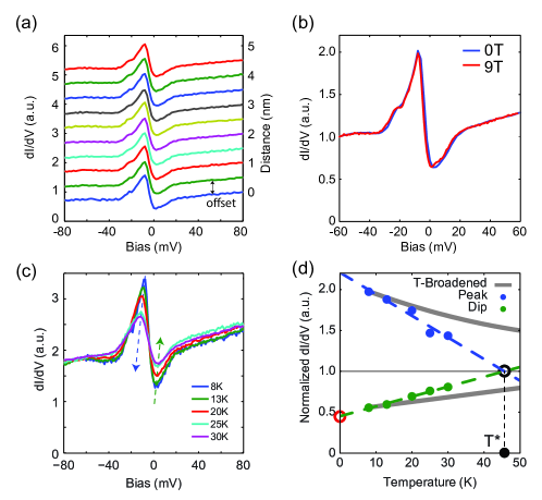
We expect that the surface is nonpolar, and may provide a better view of the bulk bands and hybridization process. On the surface, instead of the broad and inhomogeneous -28 mV feature, we observe a remarkably sharp feature centered at -8 meV (Fig. 2, which is extremely homogeneous on clean terraces of varying sizes (Fig. 3a). The state shows no change in magnetic field up to 9 T (Fig. 3b), unlike the field-suppression of the ‘in-gap’ state observed by NMR.Caldwell et al. (2007) A similar state has been seen by some ARPES experiments, weakly dispersing around -8 mV to -4 mV, and has been claimed as the ‘in-gap’ signature of a TKI.Miyazaki et al. (2012); Neupane et al. (2013) On the contrary, we will argue based on its temperature dependence that the -8 mV feature is the hybridized - band itself, observed specifically on the surface and possibly representative of the bulk.
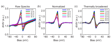
Figure 3c shows substantial reduction in spectral weight of the -8 mV peak between 8 K and 30 K. To determine whether the reduction could be ascribed to thermal broadening alone, we compare the maximum value of the normalized spectra at each temperature to the maximum value of a thermally broadened 8 K spectrum in Fig. 3d. It is clear that the spectral peak of the raw data decreases substantially faster than would be expected from thermal broadening alone, and will be completely suppressed by 40 - 50 K. We similarly extrapolate that the associated Fermi level gap will be completely filled by 40 - 50 K. This temperature scale is consistent with the reported where previous experiments have observed a sharp increase in resistivity,Menth et al. (1969) a sign change of the Hall coefficient,Allen et al. (1979) a change in the magnetic susceptibility,Caldwell et al. (2007) and an abrupt change in Sm valence from 2.50.Mizumaki et al. (2009) This coincident temperature dependence confirms that the -8 mV state is intimately related to the band hybridization.
‘In-gap’ states. Although the spectral gap width uniformly exceeds 20 meV, we observe residual spectral weight in the gap on all four surfaces. Temperature dependent spectroscopy on the surface allows extrapolation of the gap minimum to K to check whether the in-gap spectral weight is consistent with simple thermal excitation. Figure 3d shows that even at zero temperature, the extrapolated minimum is nonzero and approximately half the background conductance. This contrasts with a two-channel tunneling model of a clean Kondo insulator in which the hybridization gap should completely suppress the Fermi level tunneling conductance at K.Maltseva et al. (2009); Figgins and Morr (2010) Furthermore, unlike previous STM observations of hybridization gap development in other heavy fermion materials,Schmidt et al. (2010); Ernst et al. (2011); Aynajian et al. (2012) the surface of SmB6 measured in Fig. 3c is free from quantum critical fluctuations, impurities, or structural defects, which would increase the self-energy and move spectral weight into the gap.Wölfle et al. (2010) Our observation of zero bias tunneling conductance are consistent with the in-gap surface states of a TKI recently suggested by other experiments,Jiang et al. (2013); Li et al. (2013); Kim et al. (2013) but we cannot exclude the possibility of topologically trivial surface states.Frantzeskakis et al. (2013)
Discussion
It is well known that tunneling into a Kondo impurity – a single magnetic atom in a non-magnetic host – reflects the impurity level, the conduction band, and the quantum mechanical interference between those two tunneling channels. The interference manifests as a Fano resonance – an asymmetric dip-peak feature – which dominates the tunneling signal.Madhavan et al. (1998) Similarly in Kondo lattice systems, the interference effect may dominate the differential tunneling conductance, giving an asymmetric dip-peak but obscuring the underlying DOS.Yang (2009); Maltseva et al. (2009); Figgins and Morr (2010); Wölfle et al. (2010); Benlagra et al. (2011) Here we will separate the three components of the STM-measured on SmB6 and show that it is dominated by the bare DOS.
The differential tunneling conductance can be modeled as
| (1) |
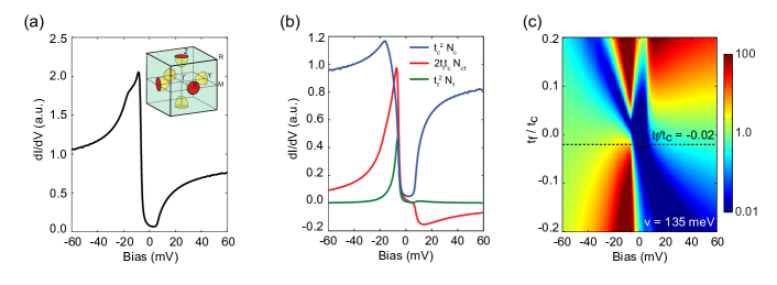
where and are the imaginary parts of the conduction and band Green’s functions, and are the respective tunneling amplitudes, and represents the quantum mechanical interference between the two tunneling channels.Figgins and Morr (2010); Wölfle et al. (2010); Benlagra et al. (2011); Aynajian et al. (2012) Guided by ARPES,Jiang et al. (2013) we model the conduction band as an ellipsoid centered at the point, shown schematically in the inset to Fig. 4a, and the states as a flat band whose energy depends on the chemical potential at the surface. We vary the band energy , tunneling ratio , and hybridization amplitude to find the best match to our data, shown in Fig. 4a.Sup The fit qualitatively reproduces the peak position, peak shape, and gap width in the data. The scaled components , , and are separately plotted in Fig. 4b, thus giving access to the bare hybridized DOS in and . Both show a dominant peak on the filled state side, in accordance with the electron-like conduction band.Miyazaki et al. (2012); Xu et al. ; Jiang et al. (2013); Neupane et al. (2013); Frantzeskakis et al. (2013) Because the ratio depends on the details of the tunnel junction, we show in Fig. 4c the dependence of on . For positive , a prominent peak from the interference term appears on the empty state side, consistent with PTS and PCS data.Amsler et al. (1998); Zhang et al. (2013) In fact, given the ARPES-measured bulk band structure, the Green’s functions of Fig. 4b show that a positive bias peak can come only from , suggesting that PTS/PCS experiments are dominated by the interference rather than the bare DOS. The dip apparent in PTS/PCS data may therefore represent an energy range of destructive interference, and not necessarily the hybridization gap. But for all four surface morphologies in Figs. 2e-h, we find the more prominent peak on the filled state side of the spectral gap, consistent with expectations for the bare DOS, suggesting that the STM-observed spectral gap is representative of the true hybridization gap. Furthermore, throughout this tunneling regime, the modeled differential conductance is vanishingly small within the hybridization gap, in contrast to the in-gap spectral weight we observe on all four surfaces.
We use the spatial resolution of STM to reconcile some apparent discrepancies between ARPES experiments.Miyazaki et al. (2012); Xu et al. ; Jiang et al. (2013); Neupane et al. (2013); Frantzeskakis et al. (2013) ARPES, with typical spot size on the order of hundreds of microns, measures signatures of all surfaces simultaneously. We expect that most ARPES experiments will show momentum-resolved contributions from both the Sm-terminated and surfaces (Figs. 2a-b), and possibly the top few layers of the bulk, but not from the two disordered surfaces where is a poor quantum number (Figs. 2c-d). Depending on the fractional composition of the cleaved surface structure, as well as the photon energy, depth probed, and detector resolution, ARPES may observe the spatial average of the -28 mV and -8 mV bands from the Sm-terminated surfaces as a single broadened band at intermediate energy,Xu et al. ; Jiang et al. (2013) or as oneFrantzeskakis et al. (2013) or twoMiyazaki et al. (2012); Neupane et al. (2013) separate states. In the latter scenario, the -8 mV band has been interpreted as an ‘in-gap’ state.Miyazaki et al. (2012); Neupane et al. (2013) However, we note that a topological in-gap state would be expected to span the upper and lower hybridized bands, and thus would appear as continuous spectral weight filling the hybridization gap, rather than as a sharp peak at a specific energy. Indeed, we consistently observe broad in-gap spectral weight on all surfaces.
With these first atomically resolved spectroscopic measurements on SmB6, we provide a general new paradigm for interpreting Kondo hybridization, and lay the specific groundwork for understanding TKIs. First, our explicit decomposition of the measured tunneling conductance into DOS vs. interference channels provides an intuitive way to understand tunneling measurements of Kondo hybridization in a broad class of heavy fermion materials.Schmidt et al. (2010); Ernst et al. (2011); Park et al. (2012); Aynajian et al. (2012); Zhang et al. (2013) Second, we confirm that SmB6 is a Kondo insulator, by using this decomposition to reveal the full band hybridization gap, spanning the Fermi level, on all four observed surface morphologies. Our temperature dependent spectroscopy illustrates the surface hybridization process, beginning around 40-50 K, in agreement with previous bulk measurements. Third, our observation of the band shifts between polar and non-polar cleaved surfaces of SmB6 reveals the dramatically different electronic environments in which the predicted topological surface state must exist. However, we observe in-gap spectral weight significantly exceeding bulk hybridization models persisting on all surface morphologies. Theoretical modeling of bulk band shifts, surface states, and hybridization for different surface terminations is urgently needed. Our work provides the nanoscale spectroscopic details necessary for understanding the first strongly correlated topological insulator.
Methods
Single crystals of SmB6 were grown using an Al flux method,Kim et al. (2012) cleaved in cryogenic ultrahigh vacuum around 30 K, and immediately inserted into our homebuilt STM. STM tips were cut from PtIr wire and cleaned via field emission on polycrystalline Au foil. We imaged two samples, with multiple tip-sample approaches on each cleaved surface, in regions separated by many microns. Spectroscopic measurements were carried out between 2 and 30 K, in fields up to 9 T, using a standard lock-in technique with bias modulation at 1115 Hz.
Acknowledgements
We especially thank Piers Coleman, Ilya Elfimov, Rebecca Flint, Victor Galitski, Laura Greene, Dirk Morr, Wan Kyu Park, and Jason Zhu for helpful conversations. We thank Dennis Huang, Eric Hudson, and Can-Li Song for careful reading of the manuscript. We thank David Lange for help with the SEM and EBSD measurements, and Greg Lin for help with the XPS measurements. M.M.Y. acknowledges a fellowship from NSERC. The work at Harvard was supported by the US National Science Foundation under grant DMR-1106023. The work at UC Irvine was supported by NSF-DMR-0801253 and UC Irvine CORCL Grant MIIG-2011-12-8.
References
- Fu et al. (2007) L. Fu, C. Kane, and E. Mele, Physical Review Letters 98, 106803 (2007).
- Ando (2013) Y. Ando, (2013), arXiv:1304.5693 .
- Hasan and Moore (2011) M. Z. Hasan and J. E. Moore, Annual Review of Condensed Matter Physics 2, 55 (2011).
- Qi and Zhang (2011) X.-L. Qi and S.-C. Zhang, Reviews of Modern Physics 83, 1057 (2011).
- Dzero et al. (2010) M. Dzero, K. Sun, V. Galitski, and P. Coleman, Physical Review Letters 104, 106408 (2010).
- Coleman (2007) P. Coleman, Handbook of Magnetism and Advanced Magnetic Materials (2007), arXiv:0612006 .
- Takimoto (2011) T. Takimoto, Journal of the Physical Society of Japan 80, 123710 (2011).
- Lu et al. (2013) F. Lu, J. Zhao, H. Weng, Z. Fang, and X. Dai, Physical Review Letters 110, 096401 (2013).
- Menth et al. (1969) A. Menth, E. Buehler, and T. Geballe, Physical Review Letters 22, 295 (1969).
- Allen et al. (1979) J. Allen, B. Batlogg, and P. Wachter, Physical Review B 20, 4807 (1979).
- Cooley et al. (1995) J. Cooley, M. Aronson, Z. Fisk, and P. Canfield, Physical Review Letters 74, 1629 (1995).
- Zhang et al. (2013) X. Zhang, N. P. Butch, P. Syers, S. Ziemak, R. L. Greene, and J. Paglione, Physical Review X 3, 011011 (2013).
- Kim et al. (2012) D. J. Kim, S. Thomas, T. Grant, J. Botimer, Z. Fisk, and J. Xia, (2012), arXiv:1211.6769 .
- Wolgast et al. (2012) S. Wolgast, C. Kurdak, K. Sun, J. W. Allen, D.-J. Kim, and Z. Fisk, (2012), arXiv:1211.5104 .
- Kim et al. (2013) D. J. Kim, J. Xia, and Z. Fisk, (2013), arXiv:1307.0448 .
- Thomas et al. (2013) S. Thomas, D. J. Kim, S. B. Chung, T. Grant, Z. Fisk, and J. Xia, (2013), arXiv:1307.4133 .
- Li et al. (2013) G. Li, Z. Xiang, F. Yu, T. Asaba, B. Lawson, P. Cai, C. Tinsman, A. Berkley, S. Wolgast, Y. S. Eo, D.-J. Kim, C. Kurdak, J. W. Allen, K. Sun, X. H. Chen, Y. Y. Wang, Z. Fisk, and L. Li, (2013), arXiv:1306.5221 .
- Miyazaki et al. (2012) H. Miyazaki, T. Hajiri, T. Ito, S. Kunii, and S.-i. Kimura, Physical Review B 86, 075105 (2012).
- (19) N. Xu, X. Shi, P. K. Biswas, C. E. Matt, R. S. Dhaka, Y. Huang, N. C. Plumb, M. Radovic, J. H. Dil, E. Pomjakushina, A. Amato, Z. Salman, D. M. Paul, J. Mesot, H. Ding, and M. Shi, (2013) arXiv:1306.3678 .
- Jiang et al. (2013) J. Jiang, S. Li, T. Zhang, Z. Sun, F. Chen, Z. R. Ye, M. Xu, Q. Q. Ge, S. Y. Tan, X. H. Niu, M. Xia, B. P. Xie, Y. F. Li, X. H. Chen, H. H. Wen, and D. L. Feng, (2013), arXiv:1306.5664 .
- Neupane et al. (2013) M. Neupane, N. Alidoust, S. Y. Xu, T. Kondo, D. J. Kim, C. Liu, I. Belopolski, T. R. Chang, H. T. Jeng, T. Durakiewicz, L. Balicas, H. Lin, A. Bansil, S. Shin, Z. Fisk, and M. Z. Hasan, (2013), arXiv:1306.4634 .
- Frantzeskakis et al. (2013) E. Frantzeskakis, N. de Jong, B. Zwartsenberg, Y. K. Huang, Y. Pan, X. Zhang, J. X. Zhang, F. X. Zhang, L. H. Bao, O. Tegus, A. Varykhalov, A. de Visser, and M. S. Golden, (2013), arXiv:1308.0151 .
- Flachbart et al. (2001) K. Flachbart, K. Gloos, E. Konovalova, Y. Paderno, M. Reiffers, P. Samuely, and P. Švec, Physical Review B 64, 085104 (2001).
- Travaglini and Wachter (1984) G. Travaglini and P. Wachter, Physical Review B 29, 893 (1984).
- Gorshunov et al. (1999) B. Gorshunov, N. Sluchanko, A. Volkov, M. Dressel, G. Knebel, A. Loidl, and S. Kunii, Physical Review B 59, 1808 (1999).
- Nyhus et al. (1995) P. Nyhus, S. Cooper, Z. Fisk, and J. Sarrao, Physical Review B 52, R14308 (1995).
- Amsler et al. (1998) B. Amsler, Z. Fisk, J. Sarrao, S. von Molnar, M. Meisel, and F. Sharifi, Physical Review B 57, 8747 (1998).
- Alexandrov et al. (2013) V. Alexandrov, M. Dzero, and P. Coleman, (2013), arXiv:1303.7224 .
- Aono et al. (1979) M. Aono, R. Nishitani, C. Oshima, T. Tanaka, E. Bannai, and S. Kawai, Surface Science 86, 631 (1979).
- (30) See supplemental materials.
- Ozcomert and Trenary (1992) J. S. Ozcomert and M. Trenary, Surface Science 265, L227 (1992).
- Gao et al. (2010) M. Gao, F. Ma, Z.-Y. Lu, and T. Xiang, Physical Review B 81, 193409 (2010).
- Bardeen (1961) J. Bardeen, Physical Review Letters 6, 57 (1961).
- Figgins and Morr (2010) J. Figgins and D. K. Morr, Physical Review Letters 104, 187202 (2010).
- Nakagawa et al. (2006) N. Nakagawa, H. Y. Hwang, and D. A. Muller, Nature Materials 5, 204 (2006).
- Caldwell et al. (2007) T. Caldwell, A. Reyes, W. Moulton, P. Kuhns, M. Hoch, P. Schlottmann, and Z. Fisk, Physical Review B 75, 075106 (2007).
- Mizumaki et al. (2009) M. Mizumaki, S. Tsutsui, and F. Iga, Journal of Physics: Conference Series 176, 012034 (2009).
- Maltseva et al. (2009) M. Maltseva, M. Dzero, and P. Coleman, Physical Review Letters 103, 206402 (2009).
- Schmidt et al. (2010) A. R. Schmidt, M. H. Hamidian, P. Wahl, F. Meier, A. V. Balatsky, J. D. Garrett, T. J. Williams, G. M. Luke, and J. C. Davis, Nature 465, 570 (2010).
- Ernst et al. (2011) S. Ernst, S. Kirchner, C. Krellner, C. Geibel, G. Zwicknagl, F. Steglich, and S. Wirth, Nature 474, 362 (2011).
- Aynajian et al. (2012) P. Aynajian, E. H. da Silva Neto, A. Gyenis, R. E. Baumbach, J. D. Thompson, Z. Fisk, E. D. Bauer, and A. Yazdani, Nature 486, 201 (2012).
- Wölfle et al. (2010) P. Wölfle, Y. Dubi, and A. V. Balatsky, Physical Review Letters 105, 246401 (2010).
- Madhavan et al. (1998) V. Madhavan, W. Chen, T. Jamneala, M. F. Crommie, and N. S. Wingreen, Science 280, 567 (1998).
- Yang (2009) Y.-f. Yang, Physical Review B 79, 241107 (2009).
- Benlagra et al. (2011) A. Benlagra, T. Pruschke, and M. Vojta, Physical Review B 84, 195141 (2011).
- Park et al. (2012) W. K. Park, P. H. Tobash, F. Ronning, E. D. Bauer, J. L. Sarrao, J. D. Thompson, and L. H. Greene, Physical Review Letters 108, 246403 (2012).
Supplemental Material for:
Imaging the Kondo Insulating Gap on SmB6
Michael M. Yee, Yang He, Anjan Soumyanarayanan, Dae-Jeong Kim, Zachary Fisk, Jennifer E. Hoffman
I. Surface characterization
| Element | Atomic % | |
|---|---|---|
| O | 21 | .03 |
| Sm | 2 | .56 |
| C | 45 | |
| B | 24 | .34 |
| Other | 7 | .06 |
II. Spatial dependence of spectra
III. Normalization & thermal broadening
Low temperature differential conductance spectra on the surface of SmB6 show a prominent peak-dip feature that decreases with increasing temperature (main text Fig. 3c). To determine whether the peak-dip reduction is consistent with thermal broadening alone, we first normalize the spectra to remove any artifact variations in asymmetry from piezo drift, and then simulate the effect of thermal broadening on the normalized spectra. To eliminate variations in spectral asymmetry arising from piezo drift we divide each spectrum by a cubic polynomial fit to the data, excluding the energy range of the strongly -dependent peak-dip feature (-60 mV mV), as shown in Fig. S4a. The resultant normalized spectra are shown in Fig. S4b.
To study the intrinsic temperature dependence of the spectra we need to account for the thermal broadening of data acquired at different . The effect on the spectra can be expressed as the convolution of the sample density of states and the derivative of the Fermi-Dirac distribution,Nagaoka et al. (2002)
| (S1) |
Here and are the density of states of the tip and sample respectively, * represents a convolution, and the derivative of the Fermi-Dirac distribution is
| (S2) |
which has a FWHM of . Using this formalism we can change the temperature of a spectrum from the temperature at which the data was acquired, , by deconvolving the spectrum to K with , and then convolving the spectrum to an arbitrary simulation temperature . We apply this technique to the normalized K spectrum in Fig. S4b to arrive at the series of simulated spectra at in Fig. S4c.
IV. Simulating the spectra
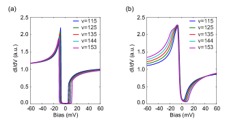
In typical STM/STS experiments, the measured differential conductance is representative of the sample density of states (DOS). However, in Kondo systems the measured represents the tunneling into the conduction band and the heavy band, as well as the quantum mechanical interference between these two tunneling channels. It is necessary to account for this cotunneling process in order to extract the underlying DOS of the hybridized bands from the spectra. We used three models to simulate our experimental spectra: a Fano modelYang (2009); Wölfle et al. (2010) as well as two Kondo lattice models.Maltseva et al. (2009); Figgins and Morr (2010) While the Fano model fails to fit the SmB6 spectra, both Kondo lattice models capture the main qualitative features of the spectra: the peak location, width, and sharpness, as well as the width and positive energy kink of the gap.
The tunneling conductance into a single ion Kondo system follows a simple Fano lineshape,Madhavan et al. (1998)
| (S3) |
where is the Fano parameter, , is the energy of the discrete -state and is the width of the resonance. The Fano lineshape is also the limiting case in Kondo lattice systems with spatial disorder or large self-energy.Wölfle et al. (2010)
To expand this to a clean Kondo Lattice system, we use both the analytic model of Maltseva, Dzero, and ColemanMaltseva et al. (2009) and the numerical model of Figgins and Morr.Figgins and Morr (2010)
Using the formalism of Figgins and Morr, we modeled the spectrum as the sum of three terms from the conduction band, the -band and the interference of the two channels:
| (S4) |
| (S5) |
where represents the DOS of the respective channel, is the ratio of the tunneling amplitudes into the -band and the conduction band, and the hybridized Green’s functions are given by
| (S6) | |||||
| (S7) | |||||
| (S8) |
The hybridized Green’s functions are expressed in terms of the hybridization amplitude and the bare Green’s functions: and where and are the unhybridized band structures of the conduction and -band, respectively. The hybridized bands take the form
| (S9) |
We modeled the Sm conduction band as an ellipsoid centered at the point of the three-dimensional Brillouin zone, with semi-major axes and eV in agreement with ARPES measurements.Jiang et al. (2013) We modeled the Sm band as a non-dispersive flat band spanning the Brillouin zone at energy . We used a self-energy for the measurement temperature K , and varied , , and to match the data. We found a good match to the main qualitative features of the data for meV, meV, and .
To verify our results we also used the model of Maltseva, Dzero and Coleman:
| (S10) |
| (S11) |
where , and are the lower and upper conduction band edges, is the width of the single ion Kondo resonance, is the hybridization amplitude, is the ratio of the tunneling amplitudes, is the energy of the non-dispersive -band and is the self-energy.Mal
We used experimental data on SmB6 to choose appropriate values for the parameters. We used eV in agreement with ARPES,Jiang et al. (2013) eV in agreement with LDA calculations,Antonov et al. (2002) giving a total conduction bandwidth of eV.Unp We used with K in agreement with the onset of a valence change.Mizumaki et al. (2009) We used for the measurement temperature K and varied , , and to match the data. We also found good match to the main qualitative features of the data for meV, meV, and . Furthermore, this value of is roughly consistent with the expected magnitude of the hybridization gap .
We summarize the three models in Figs. S5 and S6. The calculated is plotted as a function of bias and tunneling ratio/Fano parameter. All models agree on the following main features: (1) the relative prominence of a negative energy peak for and the emergence of a positive energy peak for ; (2) the persistence of a deep gap ( of the background ) near the Fermi level across a wide range of . However, the Fano model fails to capture some subtleties of the full Kondo lattice modelsZhang et al. (2013) which are seen in the data, such as the abrupt kink on the positive edge of the gap.

References
- Nagaoka et al. (2002) K. Nagaoka, T. Jamneala, M. Grobis, and M. Crommie, Physical Review Letters 88, 077205 (2002).
- Yang (2009) Y.-f. Yang, Physical Review B 79, 241107 (2009).
- Wölfle et al. (2010) P. Wölfle, Y. Dubi, and A. V. Balatsky, Physical Review Letters 105, 246401 (2010).
- Maltseva et al. (2009) M. Maltseva, M. Dzero, and P. Coleman, Physical Review Letters 103, 206402 (2009).
- Figgins and Morr (2010) J. Figgins and D. K. Morr, Physical Review Letters 104, 187202 (2010).
- Madhavan et al. (1998) V. Madhavan, W. Chen, T. Jamneala, M. F. Crommie, and N. S. Wingreen, Science 280, 567 (1998).
- Jiang et al. (2013) J. Jiang, S. Li, T. Zhang, Z. Sun, F. Chen, Z. R. Ye, M. Xu, Q. Q. Ge, S. Y. Tan, X. H. Niu, M. Xia, B. P. Xie, Y. F. Li, X. H. Chen, H. H. Wen, and D. L. Feng, (2013), arXiv:1306.5664 .
- (8) We have corrected a typo in the original Ref. Maltseva et al., 2009, which propagated into Ref. Zhang et al., 2013. The factor in the second term of the Green’s function is necessary to correctly dimensionalize the equation; its absence leads to an unphysical in a subset of parameter space.
- Antonov et al. (2002) V. Antonov, B. Harmon, and A. Yaresko, Physical Review B 66, 165209 (2002).
- (10) We note the use of unphysically small conduction bandwidth meV in Ref. Zhang et al., 2013.
- Mizumaki et al. (2009) M. Mizumaki, S. Tsutsui, and F. Iga, Journal of Physics: Conference Series 176, 012034 (2009).
- Zhang et al. (2013) X. Zhang, N. P. Butch, P. Syers, S. Ziemak, R. L. Greene, and J. Paglione, Physical Review X 3, 011011 (2013).