Elemental Topological Insulator with a Tunable Fermi Level:
Strained -Sn on InSb(001)
Abstract
We report on the epitaxial fabrication and electronic properties of a topological phase in strained -Sn on InSb. The topological surface state forms in the presence of an unusual band order not based on direct spin-orbit coupling, as shown in density functional and GW slab-layer calculations. Angle-resolved photoemission including spin detection probes experimentally how the topological spin-polarized state emerges from the second bulk valence band. Moreover, we demonstrate the precise control of the Fermi level by dopants.
Two- and three-dimensional (2D, 3D) topological insulators (TIs) owe their conductance to spin-polarized edge or surface states, respectively Qi and Zhang (2011); Kane and Mele (2005a); König et al. (2007); Fu et al. (2007). Assuming time-reversal symmetry (TRS), an inversion between occupied and unoccupied bands of different parity is usually caused by strong spin-orbit (SO) coupling, which alters the topological invariant from =0 (trivial insulator) to =1 (topological insulator) Kane and Mele (2005b); Fu and Kane (2007). This gives rise to an odd number of gapless boundary states Kane (2008). For such a state, TRS demands that electrons moving in opposite directions carry opposite spins, which are therefore protected against backscattering. They promise lossless transport and new avenues for spin-based data processing.
A number of materials were proposed as TIs based on parity inversions Fu and Kane (2007). Some have been investigated by angle-resolved photoemission (ARPES), which can directly probe the topological surface state (TSS) with its two linearly dispersing bands that cross at the Dirac point. Examples are Bi0.9Sb0.1 Hsieh et al. (2009), Bi2Se3 Xia et al. (2009), Bi2Te3 Chen et al. (2009), and Sb2Te3 Pauly et al. (2012) (Bi2X3 family). A 2D TI is predicted Bernevig et al. (2006) for HgTe quantum wells embedded in CdTe. Closely related to HgTe in terms of band structure is -Sn, which in strained form (together with HgTe) has been proposed as a 3D TI Fu and Kane (2007), however, has not yet been explored. The band order in both high-Z systems (with zero gap unless strained) is rather uncommon: The crystal symmetries together with relativistic corrections give rise to the necessary inversion of band parity - unlike in the Bi2X3 family where the SO partner bands are connected by the TSS Zhang et al. (2009).
In HgTe/CdTe quantum wells the conductivity of is explained by spin-polarized edge channels in the quantum spin Hall effect König et al. (2007); Brüne et al. (2010, 2012), giving proof of a 2D TI. A crossover to 3D has been reported for thick HgTe films, judged from odd Hall plateaus Brüne et al. (2011) as well as ARPES data of a linear surface state Brüne et al. (2011); Crauste et al. (2013). However, a direct probe of the spin character by spin-resolved photoemission (SARPES) is missing Crauste et al. (2013). Moreover, the delicate growth together with the toxicity of Hg makes handling of this system difficult.
The material in focus of the present work, -Sn on InSb, is likewise a heteroepitaxial strained system. The use of InSb as a template for high quality crystals is well established Farrow et al. (1981); Mason and Williams (1992); Magnano et al. (2002). It induces a slight compressive strain of 0.14% in the diamond lattice of -Sn. The bulk band structure of -Sn/InSb was the subject of a few photoemission reports for the (001) Höchst and Hernandez-Calderon (1983); Fantini et al. (2000a) and (111) surface Hernandez-Calderon and Höchst (1985); Fantini et al. (2000b). These early studies at low resolution, however, did not address the question of a TSS. To date, experimental and computational demonstrations are still missing.
In this Letter, we report on a 3D topological phase in strained -Sn. By comparing ARPES including spin detection with density functional theory (DFT) and GW quasi-particle calculations, we show that the topological situation emerges from an unusual band order not simply explained by SO coupling. The spin character of the TSS is probed directly, showing a counter-clockwise in-plane rotation for the occupied states of the Dirac cone. In addition, we demonstrate control of the Fermi level by adding dopants. This is the first realization of an elemental TI, which promises ease of fabrication and tuning.
-Sn samples have been synthesized in situ by molecular-beam epitaxy in ultra-high vacuum on a clean InSb(001) substrate with an additional Te dopant flux, leading to high surface quality as monitored by low-energy electron diffraction. ARPES measurements have been performed with He-I and Ne-I excitation (21.22 eV and 16.86 eV), and by tunable synchrotron radiation. Experimental details as well as the numerical procedures are described in the Supplementary Material 111supplementary material.
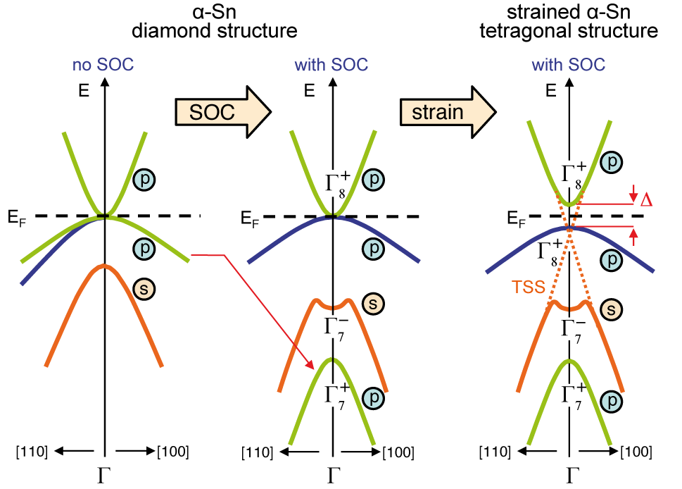
In -Sn, the band situation is different from the Bi2X3 TIs, where the SO coupling drives the parity inversion Zhang et al. (2009). The unstrained -Sncrystal is a zero-gap material in which the light-hole valence band () and the band (usually the conduction band) are inverted Groves and Paul (1963); Pollak et al. (1970) compared to other semiconductors in diamond and zinc-blende structure Harrison (1989), see band schematic in Fig. 1. The closed gap results from degenerate states at the -point, where the heavy-hole valence band and the conduction band touch each other at . The effect of SO coupling is to impose a strong downward shift (middle panel of Fig. 1), which leads to a deep-lying split-off band ().
This gives rise to the unusual band situation in -Sn: Since the SO split-off band () is even lower than the band, this latter (second) valence band can host the TSS in conjunction with the conduction band of opposite parity. In addition, there is the first valence band () in-between, representing a further modification compared to the Bi2X3 family with a direct (SO-driven) topological band pairing. Lattice strain then can lift the band degeneracy at the -point, as shown in the right panel of Fig. 1 for in-plane compressive strain (i.e. a tetragonal lattice). A small energy gap opens at while the band order remains otherwise unchanged.
The bands for bulk -Sn with the appropriate strain (0.14%) have been derived from a GW quasi-particle calculation (including SO coupling) and are displayed in Fig. 2a). The strain induces a small -point gap of 30 meV at the Fermi level. The second valence band - as the candidate to host the TSS - exhibits a weak M-shape and a maximum roughly located at 0.5 eV below . Interestingly, and unlike in Bi2X3, this carries a strong s-orbital character (rather than p-character). The third valence band (from SO coupling) is located slightly below.
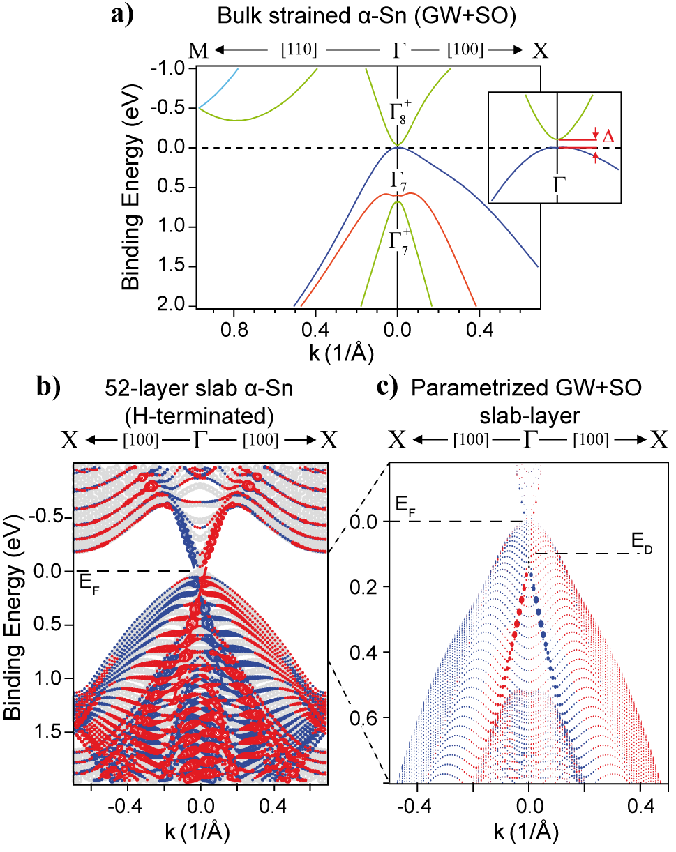
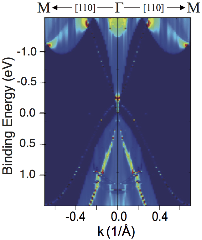
In order to generate the TSS, which requires existence of surfaces, we have performed slab-layer calculations, see Fig. 2 b), where two linearly dispersing states (on a bulk band background) are clearly discernible (unlike simple LDA, the LDA+U used here produces the correct band order, as does GW). In addition, we have evaluated the spin character, which shows a clear separation into opposite signs (fully in-plane for the main symmetry lines). The spin helicity is counter-clockwise below the Dirac point, and reversed above. Quantization effects present in small slab models can be avoided using a semi-infinite bulk connection to the surface layers, as in supplementary Fig. S1 [25]. A detailed view of the TSS is obtained from GW calculations where a tight-binding parametrization was implemented in a particularly thick slab with 256 layers. Here it becomes apparent that the TSS emerges straight from the second valence band, as assumed above based on the band parity sequence. It gives rise to a Dirac crossing at about 0.1 eV below the Fermi level.
In Fig. 3a) we present ARPES data of pristine -Sn taken with an excitation energy of h = 119 eV which corresponds approximately to the -point of the bulk BZ and, thus, compares directly to the band structure calculations of Fig. 2. We identify the and bands, which appear rather intense at this photon energy. Interestingly, the band looses much of its intensity close to normal emission, i.e., k = 0, which is caused by parity-related matrix elements and, thus, directly reflects the uneven parity at . However, the linearly dispersing feature seen in our DFT calculations is not resolved at 119 eV in this sample.
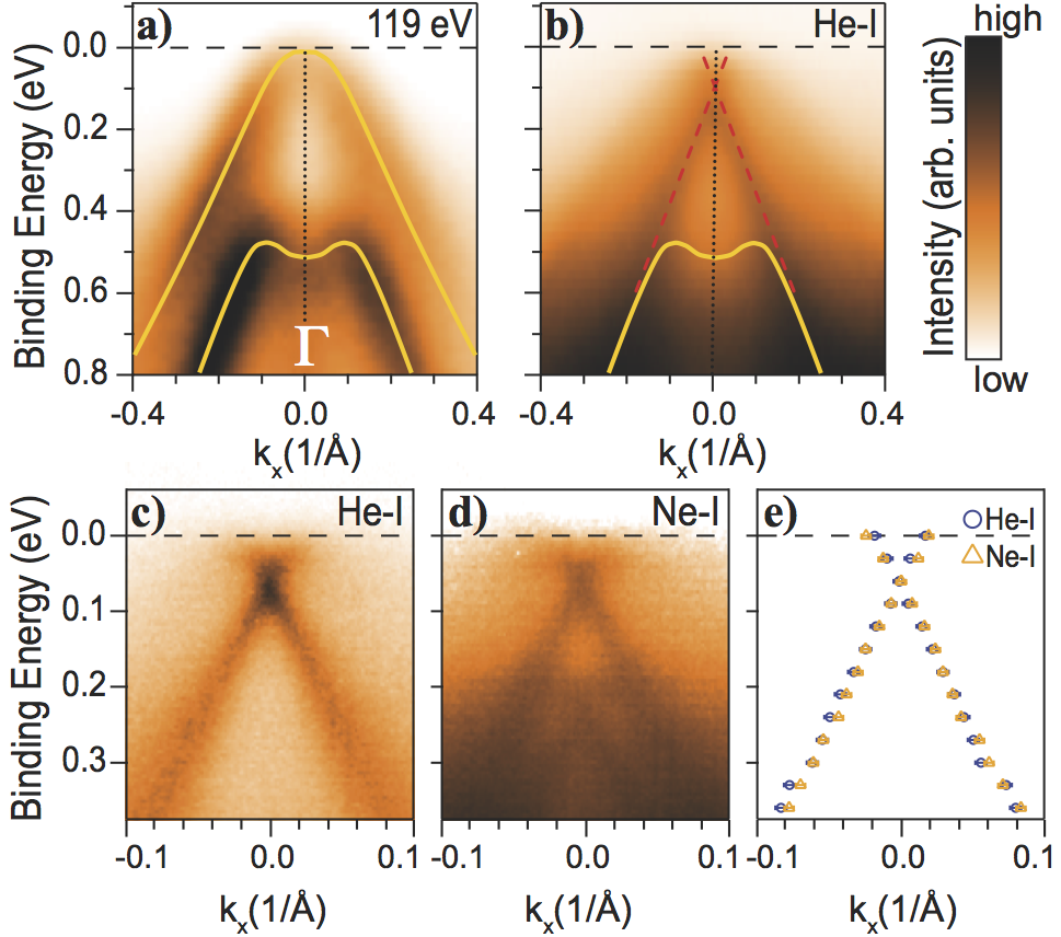
The situation changes drastically at h = 21.22 eV which gives a better observation condition for the sought-after linear feature (Fig. 3b). Additionally, the sample of Fig. 3b) has an increased surface quality as compared to the one of Fig. 3a), since Te which acts as a surfactant was added during the growth, as discussed below. The change of h adjusts the perpendicular momentum of the photoelectrons kz close to the X-point of the bulk BZ. The -valence band is smeared out to a weak background intensity but, centered around of the surface BZ, we now find a prominent feature that seems to cross with a rather linear dispersion. In addition, the close-up in Fig. 3c) suggests a crossing of the two visible branches at a binding energy of 60 meV. In agreement with our calculations presented in Fig. 2, the state emerges out of the -valence band, suggesting that it is indeed a TSS.
We can experimentally justify this suggestion further, as we characterize the feature to be a 2D surface state by changing the photon energy to h = 16.86 eV (Fig. 3d). A surface state should be unaffected by this change as it shows no dispersion perpendicular to the surface. Indeed, as we quantify by an overlay of the fitted momentum distribution curve (MDC) peak positions (Fig. 3e), the state is essentially unaltered by this change.
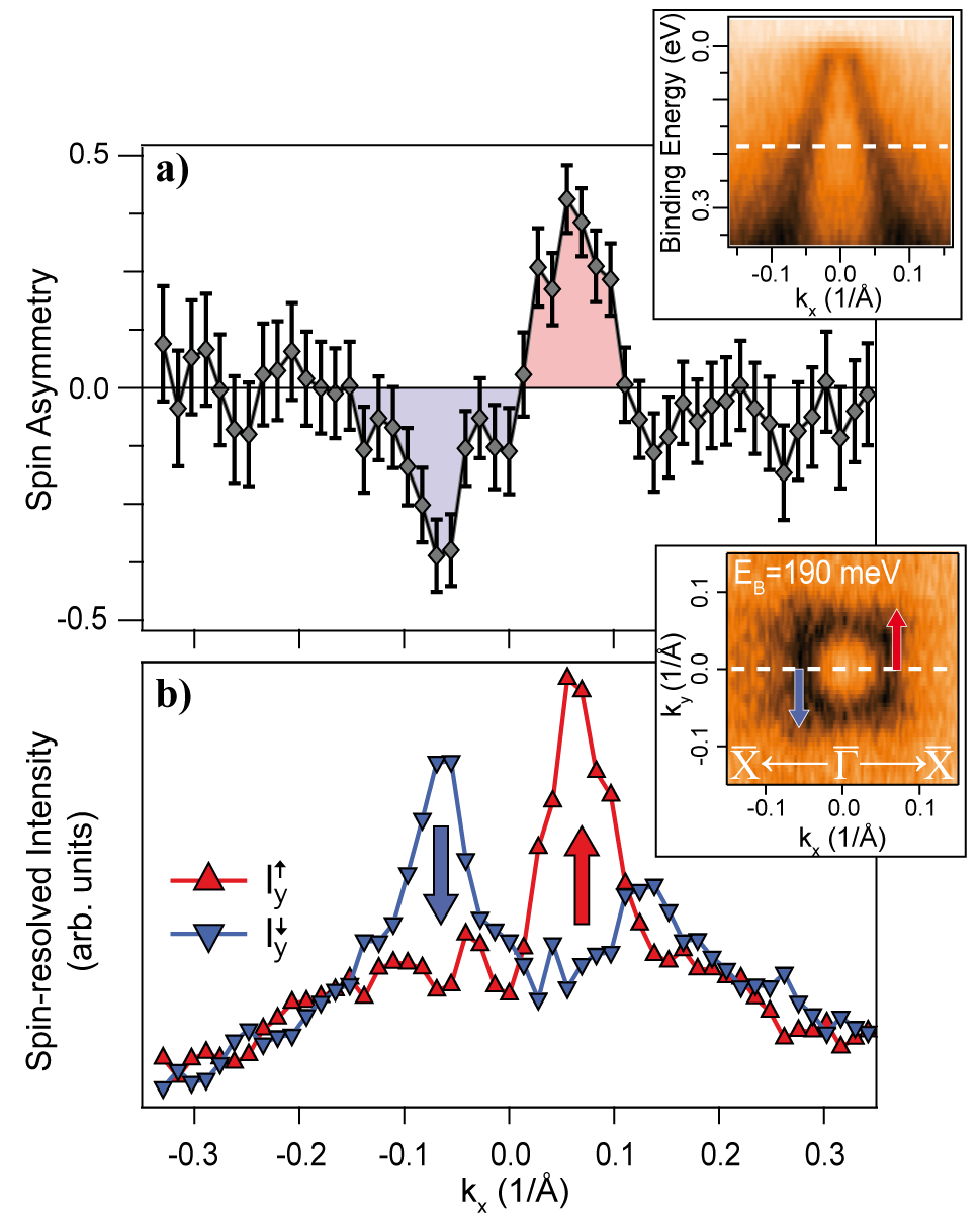
Hence, we find the linear state to satisfy key characteristics of a TSS that are surface localization and metallicity. Final evidence is obtained from the spin-polarization of the surface state. For a TI the two branches of the state should show opposite spin-polarization, in agreement with time-reversal symmetry. In Fig. 4, we present our results from spin-resolved photoemission measurements on -Sn. A MDC at = 190 meV, as marked in the upper inset of Fig. 4, reveals a strong spin-asymmetry when Mott-polarimetry is applied to the photoelectrons (Fig. 4a). We observe two features of opposite sign which match very well with the peak positions of the TSS in k-space. This leads to a spin-resolved intensity distribution where the state at k has spin along +ky while the state at k has spin along -ky (Fig. 4 b).
While we have measured all three spatial components of the spin vector Dil (2009), we limit our presentation to the y-component, as the polarization lies, within the error of the measurement, fully in this direction. Since the MDC is taken along the kx direction this means that the spin is oriented perpendicular to the momentum along the high-symmetry direction -. As sketched on the constant energy surface at = 190 meV (lower inset of Fig. 4) the sign of the spin-vector is such that the helicity is counter-clockwise below the Dirac point, in agreement with our own DFT calculations and findings in other TIs Souma et al. (2011); Pan et al. (2011); Pauly et al. (2012).
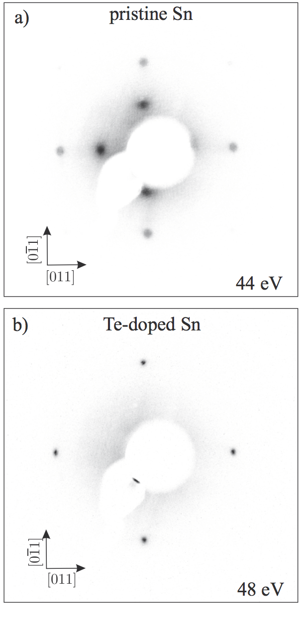
Finally, we want to address the role of the Te adatoms during the growth of our samples. As observed by low energy electron diffraction (see supplementary Fig. S2 [25]), the overall surface quality of our samples is increased as Te is added. This indicates that Te acts as a surfactant during the growth of -Sn films, similar to findings in Ge epitaxy Sakata et al. (2000). The benefit of Te for the surface quality is further underpinned by the fact that we where not able to observe the TSS in samples without any Te added as in Fig. 3 a). We speculate that a minor surface quality smears out the TSS in our photoemission experiment similar to observations in Bi2Se3 Hatch et al. (2011).
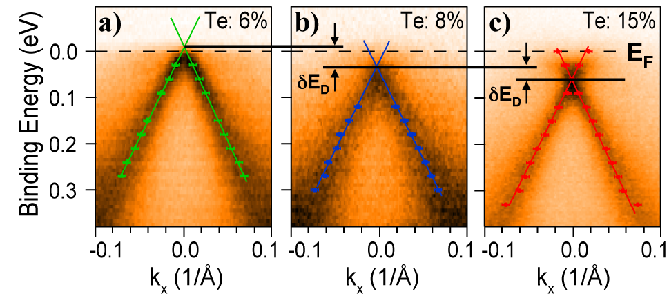
Importantly, we find that Te acts as an electron-donor which we demonstrate by dispersions measured on three samples with different Te concentrations (Fig. 5). The concentration is controlled by the Te flux during the growth and determined by core-level intensity ratios of Sn and Te. By increasing the Te concentration from 6% (Fig. 5 a) to 15% (Fig. 5 c), we can shift the position of the Dirac-point from 10 meV above to 60 meV below . We attribute the slight p-doping at low Te concentrations to a diffusion of In atoms from the substrate into the sample.
In conclusion, we have established the 3D topological insulator phase in strained -Sn by means of spin- and angle-resolved photoemission accompanied by ab initio theoretical calculations. We find good overall agreement to relativistic LDA+U as well as GW quasi-particle calculations. Our results show that the band order in -Sn is different from the known TIs of the Bi2X3 family of materials. As a consequence, a surface state emerges out of the second lowest -valence band that shows all characteristics of a TSS.
The close similarity of the -Sn bulk band structure to HgTe makes our system a promising candidate to exhibit the quantum spin Hall effect, if the film thickness is reduced to the 2D limit. In this context, it may be important to note that very recently, Sn monolayers were suggested to exhibit the quantum spin Hall insulator phase with a bulk band gap similar to 300 meV which would allow room temperature applications Xu et al. (2013). Moreover, the underlying diamond lattice of -Sn and the fact that it is the first realization of an elemental topological insulator opens up easier pathways of engineering future devices.
We are grateful for discussion with Oliver Rader and Laurens Molenkamp. This work was supported by the Deutsche Forschungsgemeinschaft under grants FOR 1162 and SCHA 1510/5-1.
References
- Qi and Zhang (2011) X.-L. Qi and S.-C. Zhang, Rev. Mod. Phys. 83, 1057 (2011).
- Kane and Mele (2005a) C. L. Kane and E. J. Mele, Phys. Rev. Lett. 95, 226801 (2005a).
- König et al. (2007) M. König, S. Wiedmann, C. Bruene, A. Roth, H. Buhmann, L. W. Molenkamp, X.-L. Qi, and S.-C. Zhang, Science 318, 766 (2007).
- Fu et al. (2007) L. Fu, C. L. Kane, and E. J. Mele, Phys. Rev. Lett. 98, 106803 (2007).
- Kane and Mele (2005b) C. L. Kane and E. Mele, Phys. Rev. Lett. 95, 146802 (2005b).
- Fu and Kane (2007) L. Fu and C. L. Kane, Phys. Rev. B 76, 45302 (2007).
- Kane (2008) C. L. Kane, Nat. Phys. 4, 348 (2008).
- Hsieh et al. (2009) D. Hsieh, Y. Xia, L. Wray, D. Qian, A. Pal, J. H. Dil, J. Osterwalder, F. Meier, G. Bihlmayer, C. L. Kane, Y. S. Hor, R. J. Cava, and M. Z. Hasan, Science 323, 919 (2009).
- Xia et al. (2009) Y. Xia, D. Qian, D. Hsieh, L. Wray, A. Pal, H. Lin, A. Bansil, D. Grauer, Y. S. Hor, R. J. Cava, and M. Z. Hasan, Nat. Phys. 5, 398 (2009).
- Chen et al. (2009) Y. L. Chen, J. G. Analytis, J.-H. Chu, Z. K. Liu, S.-K. Mo, X.-L. Qi, H. J. Zhang, D. H. Lu, X. Dai, Z. Fang, S. C. Zhang, I. R. Fisher, Z. Hussain, and Z.-X. Shen, Science 325, 178 (2009).
- Pauly et al. (2012) C. Pauly, G. Bihlmayer, M. Liebmann, M. Grob, A. Georgi, D. Subramaniam, M. R. Scholz, J. Sánchez-Barriga, A. Varykhalov, S. Blügel, O. Rader, and M. Morgenstern, Phys. Rev. B 86, 235106 (2012).
- Bernevig et al. (2006) B. A. Bernevig, T. L. Hughes, and S.-C. Zhang, Science 314, 1757 (2006).
- Zhang et al. (2009) H. Zhang, C.-X. Liu, X.-L. Qi, X. Dai, Z. Fang, and S.-C. Zhang, Nat. Phys. 5, 438 (2009).
- Brüne et al. (2010) C. Brüne, A. Roth, E. G. Novik, M. König, H. Buhmann, E. M. Hankiewicz, W. Hanke, J. Sinova, and L. W. Molenkamp, Nat. Phys. 6, 448 (2010).
- Brüne et al. (2012) C. Brüne, A. Roth, H. Buhmann, E. M. Hankiewicz, L. W. Molenkamp, J. Maciejko, X.-L. Qi, and S.-C. Zhang, Nat. Phys. 8, 485 (2012).
- Brüne et al. (2011) C. Brüne, C. X. Liu, E. G. Novik, E. M. Hankiewicz, H. Buhmann, Y. L. Chen, X. L. Qi, Z. X. Shen, S. C. Zhang, and L. W. Molenkamp, Phys. Rev. Lett. 106, 126803 (2011).
- Crauste et al. (2013) O. Crauste, Y. Ohtsubo, P. Ballet, P. A. L. Delplace, D. Carpentier, C. Bouvier, T. Meunier, A. Taleb-Ibrahimi, and L. Lévy, arXiv (2013), 1307.2008v1 .
- Farrow et al. (1981) R. Farrow, D. Robertson, G. Williams, A. Williams, A. Cullis, G. Jones, I. Young, and P. Dennis, J. Cryst. Growth 54, 507 (1981).
- Mason and Williams (1992) B. Mason and B. R. Williams, Surf. Sci. 273, L472 (1992).
- Magnano et al. (2002) E. Magnano, C. Cepek, S. Gardonio, B. Allieri, I. Baek, E. Vescovo, L. Roca, J. Avila, M. G. Betti, C. Mariani, and M. Sancrotti, J. Electron Spectrosc. Relat. Phenom. 127, 29 (2002).
- Höchst and Hernandez-Calderon (1983) H. Höchst and I. Hernandez-Calderon, Surf. Sci. 126, 25 (1983).
- Fantini et al. (2000a) P. Fantini, M. G. Betti, C. Mariani, E. Magnano, M. Pivetta, and M. Sancrotti, Surf. Sci. 454-456, 807 (2000a).
- Hernandez-Calderon and Höchst (1985) I. Hernandez-Calderon and H. Höchst, Surf. Sci. 152-153, 1035 (1985).
- Fantini et al. (2000b) P. Fantini, S. Gardonio, P. Barbieri, U. del Pennino, C. Mariani, M. G. Betti, E. Magnano, M. Pivetta, and M. Sancrotti, Surf. Sci. 463, 174 (2000b).
- Note (1) Supplementary material.
- Groves and Paul (1963) S. Groves and W. Paul, Phys. Rev. Lett. 11, 194 (1963).
- Pollak et al. (1970) F. H. Pollak, M. Cardona, C. W. Higginbotham, F. Herman, and J. P. van Dyke, Phys. Rev. B 2, 352 (1970).
- Harrison (1989) W. A. Harrison, Electronic Structure And The Properties of Solids (Dover Publications, Inc., New York, 1989).
- Dil (2009) J. H. Dil, J. Phys.: Condens. Matt. 21, 3001 (2009).
- Souma et al. (2011) S. Souma, K. Kosaka, T. Sato, M. Komatsu, A. Takayama, T. Takahashi, M. Kriener, K. Segawa, and Y. Ando, Phys. Rev. Lett. 106, 216803 (2011).
- Pan et al. (2011) Z.-H. Pan, E. Vescovo, A. V. Fedorov, D. Gardner, Y. S. Lee, S. Chu, G. D. Gu, and T. Valla, Phys. Rev. Lett. 106, 257004 (2011).
- Sakata et al. (2000) O. Sakata, P. F. Lyman, B. P. Tinkham, D. A. Walko, D. L. Marasco, T. L. Lee, and M. J. Bedzyk, Phys. Rev. B 61, 91794 (2000).
- Hatch et al. (2011) R. C. Hatch, M. Bianchi, D. Guan, S. Bao, J. Mi, B. B. Iversen, L. Nilsson, L. Hornekær, and P. Hofmann, Phys. Rev. B 83, 241303 (2011).
- Xu et al. (2013) Y. Xu, B. Yan, H.-J. Zhang, J. Wang, G. Xu, P. Tang, W. Duan, and S.-C. Zhang, arXiv (2013), 1306.3008v1 .
I Supplementary Information
I.1 Theory
Density functional theory calculations have been performed employing the full-potential linearized augmented planewave method as implemented in the FLEUR-code [1]. DFT calculations in the local density approximation (LDA) or generalized gradient approximation (GGA) predict the wrong band ordering (like in HgTe Sakuma et al. (2011)) and a metallic behavior at the L-point Rohlfing et al. (1998). To correct these deficiencies, we applied the DFT+U scheme in the spirit of Cubiotti et al. Cubiotti et al. (1999) with U = 3.5 eV. Surfaces have been simulated via calculation of films of more than 50 atomic layer thickness, to achieve a decoupling of the two surfaces of the film. Different surface terminations (e.g. a p(2 1) reconstruction or a p(1 1), hydrogen and tellurium termination) lead to different (trivial) surface states, but the topological surface state (TSS) shows up as a resonance in the bulk-projected states in all cases.
Different from DFT bandstructures of finite film setups, the spectral function calculated in a semi-infinite surface geometry allows a very direct comparison with experimental data. The infinite bulk attached to one of the surface regions provides a continuous spectrum in which surface resonances and surface states can be identified as peaks protruding over the bulk background. We performed such semi-infinite calculations using the Green function embedding method Wortmann et al. (2002), with which a surface region embedded between a semi-infinite bulk substrate and a semi-infinite vacuum can be obtained, whose imaginary part yields the Bloch spectral function of the surface . Neglecting matrix element effects and more complex interactions, the Bloch spectral function integrated over the surface region is the quantity measured in ARPES. While the projected bulk states and surface resonances are easily visualized by plotting the Bloch spectral function, truly localized surface states can only be plotted after performing broadening by adding a small imaginary part to the energy due to the infinite lifetime of such states in a DFT calculation. The result of our semi-infinte calculation is presented in Fig. S1. Two linearly dispersing states, on the bulk band background, are clearly discernible.
We have also performed many-body calculations within the GW approximation of the bulk band structure of the cubic and strained -Sn. The GW corrections to band energies have been added perturbatively to the LDA band structures obtained within the plane-wave, pseudopotential method, using the Sn4+ pseudopotentials. Special care has been paid to the contribution of the atomic core charge of Sn within the GW approximation, as discussed in Fleszar and Hanke (2005). The GW bulk band structures have been parametrized according to the non-orthogonal sp tight-binding model, similary as was done in Pedersen et al. (2010), and the obtained parameters were used in calculations of the surface band structure of large slabs containing several hundreds of Sn layers.
I.2 Experiment
The growth properties of -Sn on InSb(001) have been studied extensively in the literature. A seminal paper was published by Farrow et al. Farrow et al. (1981) who reported a high structural quality from x-ray diffraction up to film thickness. The -Sn phase in the diamond lattice is the thermodynamically stable form for bulk material below C, above which the solid will transform to the metallic -phase without TI properties. However, the heteroepitaxial film growth serves to stabilize the -Sn phase up to temperatures of C Mason and Williams (1992), so that it is stable for all practically relevant temperatures, and in addition can be subjected to moderate annealing treatments if desired. The effect of the growth conditions (rate, substrate temperature, annealing) to achieve an optimized film quality is well documented Farrow et al. (1981); Mason and Williams (1992); Magnano et al. (2002).
We have performed epitaxial deposition studies by using InSb(001) substrates using commercial wafers. Prior to epitaxy, the surface is prepared by several cycles of Ar ion sputtering and thermal annealing. The formation of a surface reconstruction on InSb, i.e., a c(8 2) superstructure visible in electron diffraction, is taken as indication for long-range-order and small defect density. Epitaxy of Sn on a substrate kept at room temperature yielded the best results, leading to a (2 1)-reconstructed surface, as reported in the literature Farrow et al. (1981); Mason and Williams (1992), even without anneal. Incorporating Te as a dopant which also acts as a surfactant resulted in a (1 1) diffraction pattern of particularly good quality (Fig. S2).
Subsequent ARPES measurements were performed on a six-axis goniometer using either He-I (21.22 eV) or Ne-I (16.86 eV) discharge radiation. The photoemission data were acquired at room temperature using a SPECS Phoibos 100 imaging analyzer, typically set to meV and resolution.
Further ARPES measurements were done at beamline 7.0.1 at the Advanced Light Source and at the SIS - X09LA beamline of the Swiss Light Source. Both endstations are equipped with Scienta R4000 electron energy analyzers. Spin-resolved measurements have been carried out at the COPHEE endstation at the SIS - X09LA beamline of the Swiss Light Source.
References
- Note (1) For a programm description see http://www.flapw.de.
- Sakuma et al. (2011) R. Sakuma, C. Friedrich, T. Miyake, S. Blügel, and F. Aryasetiawan, Physical Review B 84, 085144 (2011).
- Rohlfing et al. (1998) M. Rohlfing, P. Krüger, and J. Pollmann, Physical Review B 57, 6485 (1998).
- Cubiotti et al. (1999) G. Cubiotti, Y. Kucherenko, A. Yaresko, A. Perlov, and V. Antonov, Journal of Physics: Condensed Matter 11, 2265 (1999).
- Wortmann et al. (2002) D. Wortmann, H. Ishida, and S. Blügel, Physical Review B 66, 075113 (2002).
- Fleszar and Hanke (2005) A. Fleszar and W. Hanke, Phys Rev B 71, 45207 (2005).
- Pedersen et al. (2010) T. G. Pedersen, C. Fisker, and R. V. S. Jensen, J Phys Chem Solids 71, 18 (2010).
- Farrow et al. (1981) R. Farrow, D. Robertson, G. Williams, A. Cullis, G. Jones, I. Young, and P. Dennis, Journal of Crystal Growth 54, 507 (1981).
- Mason and Williams (1992) B. Mason and B. Williams, Surface Science 262, 169 (1992).
- Magnano et al. (2002) E. Magnano, C. Cepek, S. Gardonio, B. Allieri, I. Baek, E. Vescovo, L. Roca, J. Avila, M. G. Betti, C. Mariani, and M. Sancrotti, Journal of Electron Spectroscopy and Related Phenomena 127, 29 (2002).