Strong- versus Weak-Coupling Paradigms for Cuprate Superconductivity
Abstract
Absolute resistivity measurements as a function of temperature from optimally doped YBa2Cu3O7-δ, La2-xSrxCuO4, Bi2Sr2Ca1Cu2O8-x, and (Ca0.1La0.9)(Ba1.65La0.35)Cu3Oy thin films are reported. Special attention is given to the measurement geometrical factors and the resistivity slope between and . The results are compared with a strong coupling theory for the resistivity derivative near , which is based on hard core bosons (HCB), and with several weak coupling theories, which are BCS based. Surprisingly, our results agree with both paradigms. The implications of these findings and the missing calculations needed to distinguish between the two paradigms are discussed.
Two major discoveries were made at a very early stage in the study of cuprate superconductivity. One was the Uemura relation for underdoped samples UemuraPRL89 . This relation states that , where is the superconducting transition temperature, and is the magnetic penetration depth at zero temperature. This relation was found using the muon spin rotation (SR) technique. The second discovery was that for under doping and optimal doping, at temperatures above the resistivity is a linear function of AndoPRL04 ; BarisicCM . Near optimal doping, is similar to and the linear relation extends down to . Later on Homes extended the Uemura relation and showed that a broader scaling holds for both underdoped, optimally doped, and overdoped samples: where is the superfluid density at zero temperature, and is the conductivity at HomesPRB05 . This observation was based on optical conductivity measurements. In many low doping models, BernardetPRB02 . Therefore, the Homes law can be expressed as For both Homes and Uemura’s laws to coexist, must be universal for all underdoped cuprates.
Two kinds of theories address the Homes law. The first kind was provided by Tallon et al. TallonPRB06 , and the latter by Imry, Strongin, and Homes ImryPRL12 , and by Kogan KoganCM13 . They predict
| (1) |
where ranges from , as in the original Homes law, to . These theories have a few elements in common. They assume weak coupling (WC), that the resistivity arises mainly from disorder, that the BCS relation between the superconducting gap and the critical temperature is correct, and that the constant of proportionality (which varies a bit between authors) is on the order of unity. The big advantage of these theories is that they explain materials of all dopings. The disadvantage is that they treat a compound such as optimally doped YBCO as a dirty superconductor. In optimally doped YBCO, the resistivity extrapolates to zero at (see below), which can only occur in the absence of impurities. In fact, no experiment shows inhomogeneities in this compound OferPRB06 . In addition, the weak coupling theories do not address the temperature dependence of for , which is very different from simple metals GarlandPRL68 .
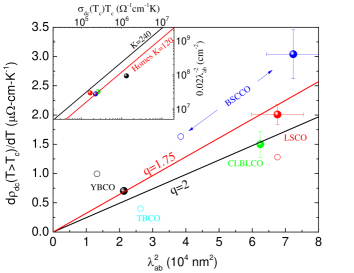
The second theory was provided by Lindner and Auerbach (LA) LindnerPRB10 . They derived the relation using the hard core boson (HCB) model at half boson filling (optimal doping); is the boson charge in units of and is the Boltzmann constant. The HCB model is expected to be valid for temperatures lower than , where Cooper pairs are supposed to start forming in the cuprates. This theory assumes a clean system and that the resistivity arises from strong coupling (SC) between bosons. The LA derivation generates the Homes law for optimal doping; it also captures the linear resistivity and provides the coefficient of proportionality quantitatively. However, the theory is not valid for an underdoped or overdoped compound, which is a serious disadvantage. Due to impurities, the extrapolation to of is finite in some cuprates. Therefore, it is more practical to write the LA law in a differential form
| (2) |
In this work, we check both the WC and SC theories, as accurately as possible, in the small region where both are valid, namely, optimal doping. We use direct current (dc) resistivity versus measurements in films of YBa2Cu3O7-δ (YBCO), (Ca0.1La0.9)(Ba1.65La0.35)Cu3Oy (CLBLCO), La2-xSrxCuO4 (LSCO), and Bi2Sr2Ca1Cu2O8-x (BSCCO). We take the geometrical factors of the film into account and check their influence experimentally. This allows us to determine in absolute value, and to demonstrate that our results are indeed film-geometry independent. We then compare to and to , as in the SC and WC theories, respectively. is taken from Refs. JacksonPRL00 , KerenSSC03 , lsco , and ProzorovApplPhysLett00 respectively; the scatter in values as provided by different authors is incorporated in the error bars as described below. Our main results, given in Fig. 1, are represented by the solid symbols. For comparison we also show for single crystals of YBCO, LSCO, BSCCO and Tl2Ba2CuO6+δ (TBCO) taken from Refs. AndoPRL04 , AndoPRL04 , WatanabePRL97 , and CarringtonPRB95 respectively, versus for single crystal taken from Refs. KieflPRB10 , lsco , TallonPRB06 and TallonPRB06 respectively (open symbols).
In the case of the LA law, we fit our data to a straight line given by Eq. 2 with as a fit parameter. We find . The fit is shown in Fig. 1. We also depict in the figure the LA prediction with . The experimentally determined boson charge of is very similar to theoretical charge of . It means that the HCB model is self-consistent for the cuprates, and a very good starting point for understanding the conductivity of optimally doped samples. We also present our results as a Homes-type plot in the inset of Fig. 1. Since optical conductivity measures the plasma frequency which is proportional to it leaves one free parameter. To achieve the same scales as Homes we multiply by . This correction is due to the difference in the penetration depth and DC conductivity as estimated by optical conductivity measurements and the techniques used here DordevicNSR13 . With this scale we find that on a log-log plot our data are not far from Homes’, which are represented by the solid line. We also show the WC theoretical predictions with in Eq. 1.
It seems that both WC and SC theories are in agreement with our experiment. Another important piece of information is the indication of carriers with charge around the superconducting-insulator transition. This indication comes from doping-temperature scaling relations of the resistivity BollingerNature11 . The emerging picture is that the superconducting state in the cuprates is grainy, sometimes called Bose glass BollingerNature11 . The SC HCB model is a good starting point for describing each grain. The normal metal between grains, in underdoped and possibly overdoped samples, plays an important role in determining the conductivity above the global . This metal is best described by one of the WC theories. However, at optimal doping one grain takes over the entire sample. When this happens the conductivity is related only to the superconducting properties, as Eq. 2 predicts.
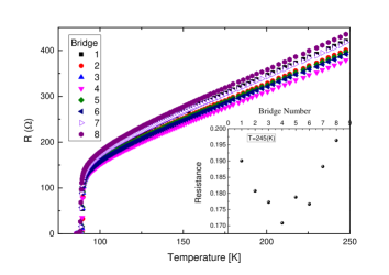
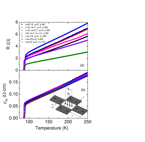
We now describe our experiment in more detail. A cardinal aspect of our measurement is the determination of the absolute value of the resistivity and resistivity derivative near . One strategy is to use single crystals, but in this case one does not know exactly which route the current takes in the sample between contacts, and it is difficult to precisely determine the resistivity. Therefore, such measurements are usually done by preparing a film and patterning a bridge on it by ion milling. It is then assumed that the resistance is dominated by the bridge. However, in high temperature superconductors, close to , the situation is not that simple. Figure 2 shows resistance measurement for a set of identical bridges. For this and other measurements, we used films grown on a mm2 SrTiO3 (STO) substrate with the -axis perpendicular to the film. Due to flux flow resistance, the transition region from normal to the superconducting state is very rounded and it is difficult to determine . There is also variation in the resistance between different bridges. This variation is due to the film being less thick near the edges. The inset of Fig. 2 shows the resistance at K as a function of bridge number. Indeed, the first and last bridges are more resistive, but the middle ones have very similar resistance. We therefore abandoned the bridge method, and focused on wide film measurements which sample the film center and have very sharp transitions, as shown in Fig. 3. However, in this case geometrical factors have to be taken into account when measuring resistivity Smits .
Our four-point probe measurement setup is shown in the inset of Fig. 3(b). The two external contacts are used as the current source and drain and the two internal contacts are the voltage probes. For a single current source at the origin in contact with a two-dimensional (2D) infinite conducting plane, the current density at a distance from the source is given by . The electric field on the conducting surface is set by . This leads to a logarithmic potential . In a current source () and drain (), with equal distance between all probes, the potential difference is For a finite sheet, the potential difference is found by introducing an infinite number of images to the original current source and drain, as shown by the spots on dark slabs in the inset of Fig. 3(b) Smits . This forces the current to run parallel to the boundary. One then sums the potential from all images. The current sources and drains, and their images, are located on a lattice given by and , where and are the width and length of the film, respectively. The potential difference between the two measured contacts is given by , where
| (3) |
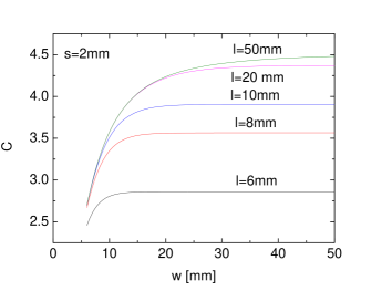
as a function of for various and a typical is shown in Fig. 4. In our set up, is on the order of . Therefore, it is essential to check that Eq. 3 is valid, as is done below. Another important factor is the film thickness , which is measured by atomic force microscopy(AFM) as shown in the inset of Fig. 5. Each of the films waw measured from all sides, and, unless stated otherwise, their thickness is nm. The resistivity is given by
| (4) |
Current simulations show that only of the total current passes close to the edges of the films where the resistance is high by (see the inset of Fig. 2). This leads to an error of less than on the resistivity due to the thickness measurement.
To check the validity of Eqs. 3 and 4, we produced YBCO films of various geometries and measured their resistance as presented in Fig. 3(a). The figure shows the resistance () of seven different films with various heights , widths , lengths and distances between contacts , in units of millimeters. Figure 3(b) depicts the resistivity obtained by Eq. 4. The resistivity is indeed geometry-independent and linear immediately above
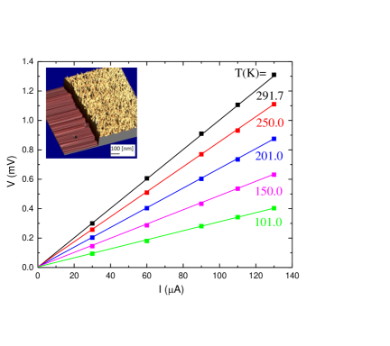
In Fig. 5, we show measurements of one of the YBCO films. In the normal state, the films show ohmic behavior up to a current of 140 A. Therefore, all our measurements are done in a current of 100.
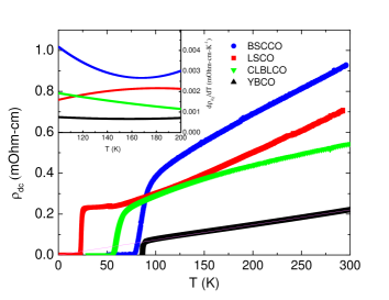
Finally, we present resistivity measurements in optimally doped films of YBCO, LSCO, BSCCO, and CLBLCO in Fig. 6. A pure linear behavior is observed only in YBCO, and, as expected, the resistivity extrapolates to zero at zero temperature. In LSCO, the substrate reduces from the bulk value considerably, due to a mismatch in lattice parameters. This lattice mismatch also reduce the of the other compounds but not as much as in LSCO. To simplify our analysis, we focus on the temperature range 100 to 200 K, which, for all materials, is higher than , higher than the region of fluctuating superconductivity, and lower than . In this temperature range, the reduction of in LSCO is not relevant. In the inset of Fig. 6, we present the first derivative of the resistivity as a function of temperature. As expected, the derivative is a constant only for YBCO. For the other materials, the derivative varies slowly with temperature. We treat the derivative as a statistical variable and assign to each material an averaged resistivity slope and standard deviation over the entire plotted range. The standard deviation is used to generate the error bars. The summary of our thermal derivative of the resistivity versus magnetic penetration depth results is plotted in Fig. 1. As mentioned before, the penetration depth is taken from the literature. For optimally doped YBCO film, nm was determined in a theory-free method using slow muons JacksonPRL00 . In this case, the value of agrees with coated samples resonance (CSR) measurements, which is also a theory-free method ProzorovApplPhysLett00 , and the error bar is known. For YBCO crystal was also measured with slow muons KieflPRB10 . For LSCO, there are only crystal measurements and all values reported are scattered around nm lsco . For BSCCO, the nm value was taken from CSR with its error bar ProzorovApplPhysLett00 . For BSCCO and TBCO crystals the value of and respectively are from Ref. TallonPRB06 . They have been measured by a few techniques but no error bar is assigned. Finally, CLBLCO was measured only by standard SR where the determination of nm involves theoretical arguments and the error bar is not known KerenSSC03 .
A comparison between our experimental results and both WC and SC theories show that both are valid for optimally doped samples to some extent. To distinguish between the two the WC theories should be extended to provide . Similarly, the SC theory should be broadened to include the doping dependence of ). We believe that there is room for a third theoretical approach that combines the two paradigms into one, in order to account for the full doping and temperature variations. As for optimal doping, the fact that the resistivity above is determined by the superconducting quantity only is an amazing property of the cuprates.
We would like to thank Gad Koren for the use of his film preparation laboratory. In addition we are grateful for helpful discussions with N. H. Lindner, A. Auerbach, and Y. Imry. This research was funded by the Israeli Science Foundation.
References
- (1) Y. J. Uemura, G. M. Luke, B. J. Sternlieb, J. H. Brewer, J. F. Carolan, W. N. Hardy, R. Kadono, J. R. Kempton, R. F. Kiefl , S. R. Kreitzman, P. Mulhern, T. M. Riseman, D. Ll. Williams, B. X. Yang, S. Uchida, H. Takagi, J. Gopalakrishnan, A. W. Sleight, M. A. Subramanian, C. L. Chien, M. Z. Cieplak, G. Xiao, V. Y. Lee, B. W. Statt, C. E. Stronach, W. J. Kossler, and X. H. Yu, Phys. Rev. Lett. 62, 2317 (1989).
- (2) Y. Ando, S. Komiya, K. Segawa, S. Ono, and Y. Kurita, Phys. Rev. Lett 93, 267001 (2004).
- (3) N. Barišić, Y. Li, G. Yu, X. Zhao, M. Dressel, A. Smontara, and M. Greven, PNAS 110, 12235 (2013).
- (4) C. C. Homes, S. V. Dordevic, T. Valla, and M. Strongin, Phys. Rev. B 72, 134517 (2005).
- (5) K. Bernardet, G. G. Batrouni, J.-L. Meunier, G. Schmid, M. Troyer, and A. Dorneich, Phys. Rev. B 65, 104519 (2002).
- (6) J. L. Tallon, J. R. Cooper, S. H. Naqib, and J. W. Loram, Phys. Rev. B 73, 180504 (2006).
- (7) Y. Imry, M. Strongin, and C. C. Homes, Phys. Rev. Lett. 109, 067003 (2012).
- (8) V. G. Kogan cond-mat/1305.3487.
- (9) R. Ofer, S. Levy, A. Kanigel, and A. Keren, Phys. Rev. B 73, 012503 (2006).
- (10) J. C. Garland and R. Bowers, Phys. Rev. Lett. 21, 1007 (1968).
- (11) N. H. Lindner and A. Auerbach, Phys. Rev B 81, 054512 (2010).
- (12) T. J. Jackson, T. M. Riseman, E. M. Forgan, H. Glückler, T. Prokscha, E. Morenzoni, M. Pleines, Ch. Niedermayer, G. Schatz, H. Luetkens, and J. Litterst, Phys. Rev. Lett. 84, 4958 (2000).
- (13) A. Keren, A. Kanigel, J. S. Lord, and A. Amato, Solid State Communications 126, 39 (2003).
- (14) Q. Li, M. Suenaga, T. Kimura, K. Kishio, Phys. Rev. B 47, 2854 (1993); C. Panagopoulos, B. D. Rainford, J. R. Cooper, W. Lo, J. L. Tallon, J. W. Loram, J. Betouras, Y. S. Wang and C. W. Chu, ibid. 60, 14617 (1999); F. Gao, D. B. Romero, D. B. Tanner, J. Talvacchio, and M. G. Forrester, ibid 47, 1036 (1993).
- (15) R. Prozorov, R. W. Giannetta, A. Carrington, P. Fournier, R. L. Greene, P. Guptasarma, D. G. Hinks, A. R. Banks, Appl. Phys. Lett. 77, 4202 (2000).
- (16) T. Watanabe, T. Fujii, and A. Matsuda Phys. Rev. Lett. 79, 2113 (1997).
- (17) A. Carrington, A. P. Mackenzie, D. C. Sinclair, and J. R. Cooper, Phys. Rev. B 49, 13243 (1994).
- (18) R. F. Kiefl, M. D. Hossain, B. M. Wojek, S. R. Dunsiger, G. D. Morris, T. Prokscha, Z. Salman, J. Baglo, D. A. Bonn, R. Liang, W. N. Hardy, A. Suter,4 and E. Morenzoni, Phys. Rev. B 81, 180502(R) (2010).
- (19) S. V. Dordevic, D. N. Basov, and C. C. Homes, Nat. Sci. Rep. 3, 1713 (2013)
- (20) A. T. Bollinger, G. Dubuis, J. Yoon, D. Pavuna, J. Misewich, and I. Božović, Nature (London) 472, 458 (2011).
- (21) F. M. Smits, Bell System Technical Journal 34, 711 (1958).