Electronic structure modification of Si-nanocrystals with F4-TCNQ
Abstract
We use first-principles models to demonstrate how an organic oxidizing agent, F4-TCNQ (7,7,8,8-tetracyano-2,3,5,6-tetrafluoroquinodimethane), modifies the electronic structure of silicon nanocrystals, suggesting it may enhance -type carrier density and mobility. The proximity of the lowest unoccupied level of F4-TCNQ to the highest occupied level of the Si-nanocrystals leads to the formation of an empty hybrid state overlapping both nanocrystal and molecule, reducing the excitation energy to about 0.8-1 eV in vacuum. Hence, it is suggested that F4-TCNQ can serve both as a surface oxidant and a mediator for hole hopping between adjacent nanocrystals.
pacs:
61.72.Bb, 61.80.Az, 71.55.CnI Introduction
Free-standing silicon nanocrystals (Si-NCs) are specially flexible building blocks for novel functional materials, offering the possibility of energy band engineering from infra-red to ultra-violet, multiple-exciton generation and the relaxation of the momentum conservation restriction.Pavesi and Turan (2010); Kovalev et al. (1998); Beard et al. (2007) These have opened the way for conceiving a range of new Si-based applications, such as wavelength-tunable light emitters and hybrid solar cells.Pavesi and Turan (2010); Liu et al. (2009) Silicon nanoparticles may be synthesized by gas phase methods, which combine a high industrial upscaling production potential with increased facility of size and surface chemistry manipulation.Mangolini and Kortshagen (2007); Gupta et al. (2009)
After recent advances, p- and n-type doping of free-standing silicon nanocrystals has been achieved, with P and B incorporation efficiencies close to 100%.Stegner et al. (2008, 2009); Lechner et al. (2008); Pi et al. (2008) Given the high crystal quality of the silicon nanocrystals currently produced, the electrical performance of the films is now predominantly limited by the granularity and nanoscale effects.Stegner et al. (2009) The doping of nanostructures suffers from limitations not present in bulk silicon, including dopant segregation to the surface during growth,Stegner et al. (2009) compensation by surface traps, self-purification and higher ionization energies of dopants confined in nanoparticlesStegner et al. (2009); Melnikov and Chelikowsky (2004); Iori et al. (2007) resulting from carrier confinement.Pereira et al. (2009); Chan et al. (2008) Further, for decreasing nanocrystal diameters, charge carrier scattering at the surface becomes more important, and the electronic coupling between the nanoparticles becomes a dominant factor conditioning the carrier mobility.
Here, we present a strategy which may be used to improve the electrical properties of p-type nanocrystal films. The idea is to use an oxidizing agent to attract the electrons to the interface region between neighboring nanocrystals, hence increasing the hole density in the nanocrystal core. As oxidizing agent, we have chosen the organic molecule 2,3,5,6-tetrafluoro-7,7,8,8-tetracyanoquinodimethane (F4-TCNQ), used as p-type dopant in the fabrication of organic light-emitting diodes,Pfeiffer et al. (2003); Walzer et al. (2007) which has one of the highest electron affinities amongst organic electron acceptors (5.08 eV).Kanai et al. (2009) F4-TCNQ has been used for -type transfer doping of diamondQi et al. (2007) and graphene,Pinto et al. (2009); Chen et al. (2007) and to increase the work function of copper(111) crystals.Romaner et al. (2007) Similarly, since its electron affinity is larger than the ionization energy of bulk silicon, it can be used to oxidize the silicon surface. Here we will show, using first-principles electronic structure calculations, that for Si nanocrystals, the position of the highest occupied electron state varies with the diameter , and becomes very close to the energy of the lowest unoccupied electron state of F4-TCNQ for nm. Thus, it is possible to engineer a hybrid state shared by the nanocrystal and the molecule that can serve as a bridging platform for hole transfer between adjacent nanocrystals.
II Methodology
The electronic structure of F4-TCNQ/Si-NC systems was analyzed using first-principles calculations, carried out with a density functional code (AIMPRO).Briddon and Jones (2000); Rayson and Briddon (2008)
The local density approximationBriddon and Jones (2000) was used for the exchange and correlation energy. Core electrons were accounted for by using the pseudopotentials of Hartwigsen et al.,Hartwigsen et al. (1998) whereas Kohn-Sham orbitals were expanded on a Cartesian Gaussian basis set.Goss et al. (2007) Contracted 44G* basis functions were placed on Si and H atom sites, and uncontracted ddpp, dddd and ddpp basis functions were place on C, N and F sites, respectively (see Ref. Goss et al., 2007 for a comprehensive description).
The silicon nanocrystals modeled were approximately spherical, and had the surface passivated by hydrogen. The diameters of the Si core ranged from 1.5 nm (87 Si atoms) to 3.4 nm (1063 Si atoms). For the nanocrystal total energy and electronic structure calculations, we used finite real space boundary conditions. Charge density integrations were performed using periodic boundary conditions, ensuring a minimum distance of 8 Å between replicas of the system. In the latter, the charge density was expanded in a plane wave basis set with an energy cutoff of 350 Ry.
Additionally, we investigated a composite F4-TCNQ/Si-NC system, modeled by a periodic tetragonal superlattice, with a base of one Si-NC and a F4-TCNQ molecule, having the conventional tetragonal unit cell vectors parallel to the principle axis of the nanocrystal. All atomic coordinates were relaxed using a conjugate gradient algorithm, and cell coordinates were optimized using a simplex method.
III Results
III.1 Adsorption geometry
We consider the physisorption of a single F4-TCNQ molecule on the surface of the nanocrystals. Following a previous combined theoretical and experimental study on flat (111) Si surfaces,Furuhashi and Yoshinobu (2010) we assume that adsorbed F4-TCNQ molecules lie approximately parallel to the surface of a Si-NC. Full relaxation of the atomic coordinates using a conjugate-gradient algorithm leaves the F4-TCNQ hovering over the Si-NC curved surface, with small deviations from its original 2D geometry. The hydrogen atoms at the nanocrystal surface form weak bonds with N and F atoms from the adsorbate. Thus, the shortest distance between F4-TCNQ and the Si-NC depends on the configuration of the Si-H terminations on the closest nanocrystal facet, and on its curvature. Equilibrium distances ranged between 2.3 and 3.2 Å for the different nanocrystals studied.

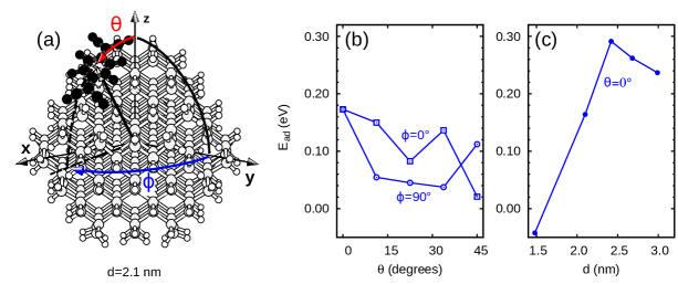
The local geometry and density of Si-H bonds of the closest Si-NC surface region has an effect on the adsorption energy, albeit with minimal impact on the electronic structure. Different orientations of the molecule relative to the principal axis of the nanocrystal can be generated by rotating the molecule by and angles around the and axis, respectively. The coordinates and are defined as the angles between geometric center of the molecule, and the and axis, respectively, as shown in Fig. 1(a). For each orientation of (defined by and ), the molecule is placed onto the surface and all the atomic coordinates allowed to relax. During relaxation, and changed by less than 1∘ for all cases.
The change in the adsorption energy with respect to molecular orientation is given in Fig. 1(b) for a nm Si-NC, for and . The adsorption energy is here defined as
| (1) |
where , and are the total energies of the isolated nanocrystal, isolated F4-TCNQ molecule, and F4-TCNQ/Si-NC system. The highest adsorption energy is found for and , when F4-TCNQ lies over the (001) facet with an adsorption energy eV. Thus, the molecule is placed in this position for all other calculations.
The adsorption energy of F4-TCNQ over the (001) facet increases with the diameter, up to about 0.2-0.3 eV [see Fig. 1(c)]. This is higher than would be expected from the presence of weak hydrogen bonds only, as weak X-HY bonds, where either X or Y have low or moderate electronegativity, have lower energies than conventional hydrogen bonds (which normally have bond energies of the order of 0.2 eVKolasinski (2001)). For larger nanocrystals, is slightly higher than for smaller nanocrystals because in addition to the electrostatic dipole-dipole interaction associated with the hydrogen bonds, there is an attraction resulting from the polarization of the nanocrystal and electron transfer to the molecule, which will be analyzed in more detail in Section III.3. This latter is absent in the smallest nanocrystal considered (1.5 nm), and increases with nanocrystal size. The slight decrease of the adsorption energy for 2.7 nm and 3.0 nm nanocrystals has a different origin. In these nanocrystals the number of SiH2 di-hydride surface units on the (001) facet is smaller, thus reducing the number of weak hydrogen bonds.
III.2 Electronic structure and local density of states

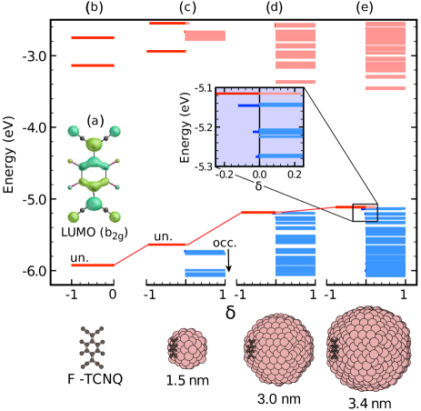
Inspection of the one-electron structure approximately represented, in the density functional theory framework, by the Kohn-Sham eigenvalues, and the contribution of each species to the respective eigenstates enlightens the changes in the electronic structure of the nanocrystals. Populations of the Kohn-Sham states (Mulliken gross populations) were obtained from the projection of the Kohn-Sham eigenstates on the basis functions.Mulliken (1955) The localization of each eigenstate () on the nanocrystal was obtained by summing over all the basis functions localized on the Si and H atoms , where is the population of level on basis function . To ease representation, the localization on the molecule is defined with the opposite sign . The analysis for nanocrystals with nm, 3.0 nm and 3.4 nm is represented in Fig. 2, where each horizontal line represents a Kohn-Sham state. The fractional localizations on the molecule () and NC () are represented as negative and positive values of , respectively. For the smaller nanocrystal ( nm), the interaction with a F4-TCNQ adsorbate is rather weak, and the electronic structure of the combined system is, in a good approximation, a superposition of the individual components. The isolated F4-TCNQ molecule has its lowest unoccupied symmetric state eV below the vacuum level [see Fig. 2(a)]. The Kohn-Sham energy level diagram in Fig. 2(b)–(e) shows that the lowest unoccupied Kohn-Sham (LUKS) state of the molecule lies above the highest occupied Kohn-Sham (HOKS) state of the nanocrystal. The next unoccupied state of the molecule, with symmetry, lies within the gap for the smallest nanocrystals only. By increasing nanocrystal diameter, however, the HOKS energy raises, the LUKS energy lowers, and the density of states increases as the sharp energy levels start forming bands. It is clear from Fig. 2 that with the increase of nanocrystal size the molecular state progressively mixes with the high lying nanocrystal occupied states, giving rise to a series of collective states that overlap both nanocrystal and F4-TCNQ atoms (see inset). For the nm nanocrystal, the population of the lowest unoccupied level of the combined system gives , indicating that a charge is being transferred.
III.3 Charge-transfer ratio
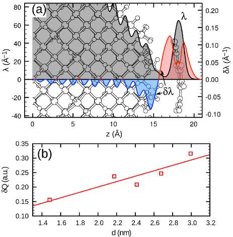
The combined system shows a displacement of the electron density () towards the the molecule. The charge displacement is better expressed with resource to an integrated electron density profile along the coordinate defined by the axis connecting the center of the nanocrystal and the center of the molecule (here taken as ),
| (2) |
Here , and define the limits of the integration box, where vanishes. The quantity is the charge in the region between the planes and . This is represented in Fig. 3(a) for the combined system. We compare the integrated electron density profiles for the composed system () with the sum of those of the individual components ( and ), for the same atomic coordinates. For all nanocrystals with 1.5 nm there is a well-defined region where
| (3) |
is negative (the oxidized region) and a region where is positive (reduced region). The charge displaced or transferred can be quantified by defining a charge transfer ratio
| (4) |
As depicted in Fig. 3(a), the region contains the molecule and its closest hydrogen atoms.

The charge transfer ratio () varies from 0.16 for =1.5 nm to 0.32 for nm. Here the basis set superposition error is about 0.01. As discussed in the previous sub-section, with increasing nanocrystal size, as the position of HOKS state of the nanocrystal raises relative to the lowest unoccupied level of the molecule, the mixing coefficients for the LUKS state shows an increasing contribution of the Si-NC states, whereas the HOKS state hows an increasing contribution of the F4-TCNQ states. Hence, increases with [Fig. 3(b)]. Further, the amount of charge transfer can be increased by adsorbing more F4-TCNQ molecules per nanocrystal. For only three F4-TCNQ molecules, the sum of the individual yields 0.87, already close to unity.
Moreover, the charge transfer ratio is most probably underestimated. It is well known that the local density approximation to the exchange energy suffers from a self-interaction error and favors delocalized over localized energy states. However, we note that the electron affinity of F4-TCNQ is underestimated. This also happens when other approximations to the exchange and correlation energy are used (see Ref.111 See EPAPS Document No. [number to be inserted by publisher] for comparative calculations of the electron affinity of F4-TCNQ. ). In contrast, the calculated work function of silicon and ionization potential of SiH4 are reproduced within 0.2 eV from experiment. Thus, the predominant source of error leads to an underestimation of the charge transfer.
III.4 Excitation energy
The excitation energy of the Si-NC with adsorbed F4-TCNQ is several times smaller than that of a bare Si-NC. An estimate for the vertical excitation energy, , may be obtained from total energy calculations:
| (5) |
where and are respectively the total energies of the combined system in the ground state and first excited state (obtained by promoting one electron to the lowest available empty state), for the ground state geometry.
The excitation energy ranges from 0.92 eV for =1.5 nm to 0.65 eV for =3.0 nm. We note that the differences between LUKS and HOKS eigenvalues are much smaller, varying between 0.09 eV for =1.5 nm and 0.01 eV for nm. Thus, the contributions to the excitation energy are the Coulomb electrostatic interaction energy, and possibly the exchange-correlation interaction energy. In fact, according to previous theoretical models for isolated Si-NCs, the difference between the excitonic gap and the independent-particle gap is dominated to a large extent by classical electrostatic contributions.Delerue et al. (1998, 2000) These include the interaction of the the electron and hole with their respective image-charge distributions, and the interaction of each one of them with the image-charge distribution of the other.
III.5 F4-TCNQ role in hole transport

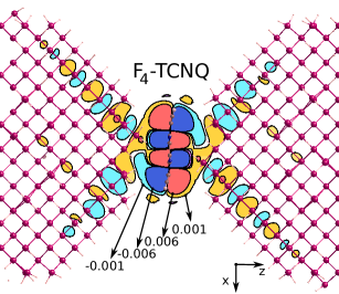
We have so far considered a model system composed of a single F4-TCNQ molecule adsorbed at the surface of one Si-NC. As a result of the overlap between the silicon orbitals and the orbitals of the molecule, electrons can be excited from the occupied hybrid electron state predominantly localized on the nanocrystal to the unoccupied hybrid electron state predominantly localized on the molecule, becoming closer in space to a neighboring nanocrystal. In a nanocrystal network, this hybrid state may provide a channel for hole transport between neighboring nanocrystals. To explore the nanocrystal-molecule interplay in this context, we used a periodic model where the nanocrystal and the molecule are repeated along the , and directions. In this superlattice, each F4-TCNQ molecule lies midway between two Si-NCs in neighboring supercells. The electron density from the lowest unoccupied state of the system is depicted in Fig. 4. The state clearly decays into the core of both nanocrystal neighbors, supporting the suggestion that it may provide an efficient pathway for electron transport. Together with the sharp decrease of the excitation energy, this result suggests that F4-TCNQ may have an extraordinary effect on the transport properties of Si-NC films.
IV Conclusions
We propose that the organic acceptor F4-TCNQ may be used to modify the electronic properties of silicon nanocrystal films. For its large electron affinity, F4-TCNQ oxidizes the nanocrystals. The amount of charge transferred is greater the larger the nanocrystal. In nanocrystals with close to 3 nm and larger, the highest occupied molecular orbitals of the nanocrystal hybridize with the LUMO state of F4-TCNQ to create a collective empty level. Such communication channel is absent, for example, in B-doped nanocrystals, where the LUMO wavefunction is confined to the nanocrystal core. The hybrid highest occupied and lowest unoccupied states are expected to improve long range charge transport across Si-NC networks.
Acknowledgements.
We thank Prof. R. Jones for his useful suggestions. This work was supported by FCT Portugal, the Calouste Gulbenkian Foundation and the Marie Curie Program REG/REA.P1(2010)D/22847, COST NanoTP, HybridSolar and Milipeia.References
- Pavesi and Turan (2010) L. Pavesi and R. Turan, eds., Silicon Nanocrystals: Fundamentals, Synthesis and Applications (John Wiley & Sons, Weinheim, 2010).
- Kovalev et al. (1998) D. Kovalev, H. Heckler, M. Ben-Chorin, G. Polisski, M. Schwartzkopff, and F. Koch, Phys. Rev. Lett. 81, 2803 (1998).
- Beard et al. (2007) M. C. Beard, K. P. Knutsen, P. Yu, J. M. Luther, Q. Song, W. K. Metzger, R. J. Ellingson, and A. J. Nozik, Nano Letters 7, 2506 (2007).
- Liu et al. (2009) C.-Y. Liu, Z. C. Holman, and U. R. Kortshagen, Nano Letters 9, 449 (2009).
- Mangolini and Kortshagen (2007) L. Mangolini and U. Kortshagen, Adv. Mater. 19, 2513 (2007).
- Gupta et al. (2009) A. Gupta, M. T. Swihart, and H. Wiggers, Adv. Func. Mater. 19, 696 (2009).
- Lechner et al. (2008) R. Lechner, A. R. Stegner, R. N. Pereira, R. Dietmueller, M. S. Brandt, A. Ebbers, M. Trocha, H. Wiggers, and M. Stutzmann, J. Appl. Phys. 104, 053701 (2008).
- Stegner et al. (2008) A. R. Stegner, R. N. Pereira, K. Klein, R. Lechner, R. Dietmueller, M. S. Brandt, M. Stutzmann, and H. Wiggers, Phys. Rev. Lett. 100, 026803 (2008).
- Stegner et al. (2009) A. R. Stegner, R. N. Pereira, R. Lechner, K. Klein, H. Wiggers, M. Stutzmann, and M. S. Brandt, Phys. Rev. B 80, 165326 (2009).
- Pi et al. (2008) X. D. Pi, R. Gresback, R. W. Liptak, S. A. Campbell, and U. Kortshagen, Appl. Phys. Lett. 92, 123102 (2008).
- Melnikov and Chelikowsky (2004) D. V. Melnikov and J. R. Chelikowsky, Phys. Rev. Lett. 92, 046802 (2004).
- Iori et al. (2007) F. Iori, E. Degoli, R. Magri, I. Marri, G. Cantele, D. Ninno, F. Trani, O. Pulci, and S. Ossicini, Phys. Rev. B 76, 085302 (2007).
- Chan et al. (2008) T.-L. Chan, M. L. Tiago, E. Kaxiras, and J. R. Chelikowsky, Nano Letters 8, 596 (2008).
- Pereira et al. (2009) R. N. Pereira, A. R. Stegner, T. Andlauer, K. Klein, H. Wiggers, M. S. Brandt, and M. Stutzmann, Phys. Rev. B 79, 161304 (2009).
- Walzer et al. (2007) K. Walzer, B. Maennig, M. Pfeiffer, and K. Leo, Chem. Rev. 107, 1233 (2007).
- Pfeiffer et al. (2003) M. Pfeiffer, K. Leo, X. Zhou, J. S. Huang, M. Hofmann, A. Werner, and J. Blochwitz-Nimoth, Org. Electron. 4, 89 (2003).
- Kanai et al. (2009) K. Kanai, K. Akaike, K. Koyasu, K. Sakai, T. Nishi, Y. Kamizuru, T. Nishi, Y. Ouchi, and K. Seki, Appl. Phys. A: Mater. Sci. Proc. 95, 309 (2009).
- Qi et al. (2007) D. Qi, W. Chen, X. Gao, L. Wang, S. Chen, K. P. Loh, and A. T. S. Wee, J. Am. Chem. Soc. 129, 8084 (2007).
- Pinto et al. (2009) H. Pinto, R. Jones, J. P. Goss, and P. R. Briddon, J. Phys.: Conden. Matter 21, 402001 (2009).
- Chen et al. (2007) W. Chen, S. Chen, D. C. Qi, X. Y. Gao, and A. T. S. Wee, J. Am. Chem. Soc. 129, 10418 (2007).
- Romaner et al. (2007) L. Romaner, G. Heimel, J.-L. Brédas, A. Gerlach, F. Schreiber, R. L. Johnson, J. Zegenhagen, S. Duhm, N. Koch, and E. Zojer, Phys. Rev. Lett. 99, 256801 (2007).
- Briddon and Jones (2000) P. Briddon and R. Jones, Phys. Stat. Sol. (b) 217, 131 (2000).
- Rayson and Briddon (2008) M. J. Rayson and P. R. Briddon, Comp. Phys. Commun. 178, 128 (2008).
- Hartwigsen et al. (1998) C. Hartwigsen, S. Goedecker, and J. Hutter, Phys. Rev. B 58, 3641 (1998).
- Goss et al. (2007) J. P. Goss, M. J. Shaw, and P. R. Briddon, Topics in Applied Physics 104, 69 (2007).
- Furuhashi and Yoshinobu (2010) M. Furuhashi and J. Yoshinobu, J. Phys. Chem. Lett. 1, 1655 (2010).
- Kolasinski (2001) K. W. Kolasinski, Surface science: foundations of catalysis and nanoscience (Wiley, Chichester, 2001), 2nd ed.
- Mulliken (1955) R. S. Mulliken, J. Chem. Phys. 23, 1833 (1955).
- Note (1) Note1, see EPAPS Document No. [number to be inserted by publisher] for comparative calculations of the electron affinity of F4-TCNQ.
- Delerue et al. (1998) C. Delerue, G. Allan, and M. Lannoo, J. Lumin. 80, 65 (1998).
- Delerue et al. (2000) C. Delerue, M. Lannoo, and G. Allan, Phys. Rev. Lett. 84, 2457 (2000).