]https://webspace.utexas.edu/ pj3292
Electronic and optical properties of GaSb:N from first principles
Abstract
GaSb:N displays promise towards realization of optoelectronic devices accessing the mid-infrared wavelength regime. Theoretical and experimental results on its electronic and optical properties are however few. To address this, we present a first principles, density functional theory study using the hybrid HSE06 exchange-correlation functional of GaSb doped with 1.6 nitrogen. To study dilute-nitrides with small band gaps, the local density approximation (LDA) is insufficient and more accurate techniques such as HSE06 are needed. We conduct a comparative study on GaAs:N, also with 1.6 nitrogen mole fraction, and find that GaSb:N has a smaller band gap and displays more band gap bowing than GaAs:N. In addition we examine the orbital character of the bands, finding the lowest conduction band to be quasi-delocalized, with a large N- contribution. At high concentrations, the N atoms interact via the host matrix, forming a dispersive band of their own which governs optoelectronic properties and dominates band gap bowing. While this band drives the optical and electronic properties of GaSb:N, its physics is not captured by traditional models for dilute-nitrides. We thus propose that a complete theory of dilute-nitrides should incorporate orbital character examination, especially at high N concentrations.
pacs:
71.15.Mb, 71.55.EqI Introduction
Dilute-nitride III-V alloys provide unique opportunities for band gap engineeringVeal et al. (2005); Belabbes et al. (2006); Harris et al. (2007). In these materials, substituting a small percentage of the column-V element with nitrogen leads to anomalous band gap bowingShan et al. (1999); Kondow et al. (1996). It is well known that N displays this interesting property due to its small size and electronegativity mismatch with the host matrix, thereby creating a localized but powerful disturbance in the host electronic potentialGueddim et al. (2007); Shan et al. (2004). While the general theory of anomalous band gap reduction in GaAs-based dilute-nitrides (GaAs:N) has been well studied, many effects and concentration regimes remain unexplored.
Moreover, GaSb:N, also a dilute nitride III-V, displays a large anomalous reduction in the band gap, due to the considerable electronegativity mismatch between N and SbBelabbes et al. (2006). This makes GaSb:N a promising material for optoelectronics accessing the 2-5 m mid-infrared wavelength regimeLindsay et al. (2008); Veal et al. (2005); Belabbes et al. (2006); Nair et al. (2012). However, despite the keen interest, reports on GaSb:N optical experiments are few and theoretical studies even fewerGueddim et al. (2007); Jefferson et al. (2006); Veal et al. (2005); Belabbes et al. (2006). The reported radiative efficiency of GaSb:N is relatively weakWang et al. (2009); Iyer et al. (2007), leading to uncertainty regarding its suitability for optoelectronic applications. In order to understand and predict its optical properties, a reliable and detailed theoretical model is essential.
In this paper, we describe an ab initio study of the electronic and optical properties of GaSb:N using density functional theory (DFT) with the accurate Heyd-Scuseria-Ernzerhof (HSE) hybrid exchange-correlation functional. We also compare the optoelectronic properties of GaSb:N with GaAs:N, the latter being well-studied and find good agreement with published GaAs:N resultsLordi et al. (2003). Moreover, we present an accurate structural analysis and a detailed study of the orbital character of the bands.
We find that at concentrations as high as 1.6, the N atoms interact with one another via the host matrix, forming a quasi-delocalized band, an effect not captured by traditional band gap bowing models. This is a vital omission since this band provides the main mechanism for band gap reduction and dominates the optoelectronic properties of GaSb:N. We see similar behaviour in GaAs:N, reported earlierLordi et al. (2003), which points to the ubiquitous nature of this phenomenon. We thus propose that the theory for dilute-nitrides should be extended to incorporate orbital character and N-N interactions, especially at N concentrations ranging from Lordi et al. (2003). Upon comparison, we notice that the optical matrix element for GaSb:N is weaker than for GaAs:N. However, with the removal of N related clusters and defects which lead to non-radiative recombination pathwaysWang et al. (2009); Kudrawiec (2011); Lindsay et al. (2008), GaSb:N could be a promising material for optoelectronic applications.

II Calculations
Ab initio calculations were performed with the Vienna-Ab Initio Simulation Package (VASP)Kresse and Hafner (1993); Kresse and Furthmüller (1996a, b) using the projector augmented wave (PAW) methodBlöchl (1994) and pseudopotentials and employing the range-separated hybrid functional of Heyd, Scuseria, and Ernzerhof (HSE06)Heyd et al. (2006). The atomic relaxations for GaSb:N were performed using the Perdew-Burke-Ernzerhof (PBE) parametrization of the generalized gradient approximation (GGA)Perdew et al. (1996, 1997). Bulk GaSb has a 2 atom primitive unit cell, while GaN0.016Sb0.984 requires a 128 atom supercell. Calculations were also extended to GaN0.008Sb0.992 (256 atoms). Starting with the experimental bulk parameters for GaSb, the supercell structures were allowed to relax until the Hellman-Feynman forces on all atoms were less than 0.01 eV/Å; the cell volume was optimized via fitting to the Birch-Murnaghan equation of state. Full relaxation using HSE06 is computationally prohibitive and was only performed on bulk GaSb. Relaxed structures for GaSb:N were obtained by using PBE to relax the atoms and using HSE06 bulk lattice parameters to estimate the relaxed volumes by extrapolation. Brillouin zone sampling for the initial LDA calculations used 444 k-mesh followed by 323 for the PBE calculations and 111 or 222 for HSE06. The energy cut off for the plane wave basis was 500 eV for hybrid calculations. Convergence was checked with respect to higher k-mesh and energy cut off values. GaN0.016As0.984, being just a reference, was relaxed using the local density approximation (LDA)Perdew and Zunger (1981) for the exchange-correlation functional.
After optimization, bulk GaSb was found to display a lattice constant of 6.16 Å which is comparable to the experimental value of 6.096 Åiof . Relaxation of N and the surrounding atoms in GaN0.016Sb0.984, GaN0.008Sb0.992, and GaN0.016As0.984 all followed the same pattern. The 4 nearest neighboring Ga atoms were pulled closer to N, to adjust to the small bond length of Ga–N. To compensate, the bond lengths for the next-neighboring shell of atoms (Sb or As) were larger than average and they approached their bulk (GaSb or GaAs) values farther away from the N atom. The Ga–N bond length in GaN0.016Sb0.984 was 2.09 Å and in GaN0.008Sb0.992 was 2.11 Å. These values are close to the bulk Ga–N bond length of 1.96 Åiof and much smaller than the bulk Ga–Sb bond length of 2.66 Å. Similarly in GaN0.016As0.984, the relaxed Ga-N bond length was 2.07 Å while the bulk Ga-As bond length is 2.45 Åiof . This gives us an idea of the large strain in the system introduced by the presence of a N atom.

III Band gaps and orbital character
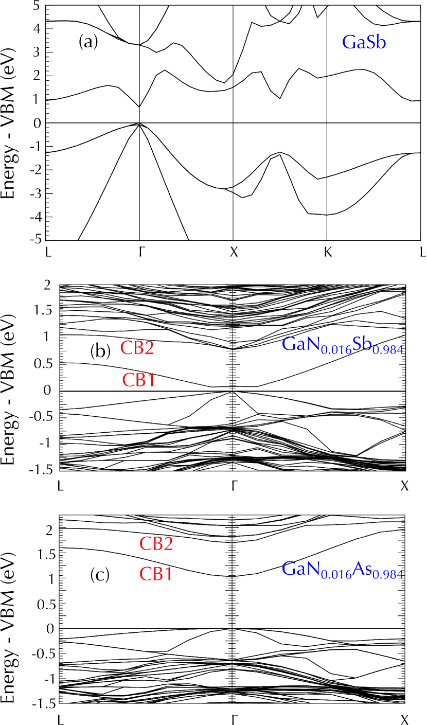
The bulk GaSb band structure using HSE06 functionals, shown in Figure 1(a), displays a band gap of 749 meV, which is remarkably close to the experimental band gap of 720 meVVeal et al. (2005). This is a testament to the accuracy of the HSE06 functional for these materials, given the well-known problem of the underestimation of band gaps by LDA/GGA. Band structure for GaN0.016Sb0.984 was also obtained (Figure 1(b)) and displays a direct gap at of 86.6 meV (reduction of 662 meV from bulk GaSb) with the L valley lower than the X, unlike a previous report which suggested an indirect gapGueddim et al. (2007). At concentrations of this gap increases to 192 meV. Experimental data for GaSb:N shows a band gap of 400 meV for Wang et al. (2009); Veal et al. (2005) and that of 500 meV for concentration. While the agreement with experiments is less stark in the latter case, it is indeed better than the negative gaps produced by LDA. For GaN0.016As0.984 the band structure is also shown (Figure 1(c)) and displays a band gap of 1.024 eV (a reduction of 400 meV from bulk GaAs). The calculated band gap is close to the experimental value of eVBi and Tu (1997) and larger than that seen for GaSb:N, as is expected. Moreover, the band gap bowing in GaSb:N is greater than that seen in GaAs:N, which is also expected. This is due to the much larger electronegativity difference between N and Sb (in GaSb:N) as compared to that between N and As (in GaAs:N) atomsVeal et al. (2005).
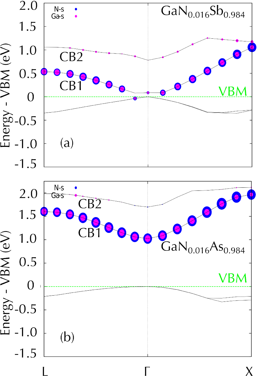
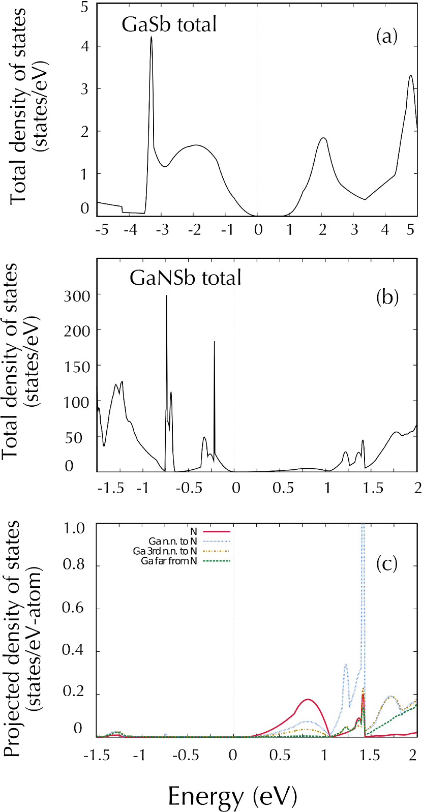
We make particular note of the nature of the conduction bands in these dilute N materials. The lowest conduction band, which we call CB1, has a wide dispersion, i.e., close to 500 meV. Moreover, this dispersion is qualitatively similar to the higher lying conduction bands (i.e. it is not a flat band as one would expect from isolated N levels). This points towards the quasi-delocalized nature of CB1. To study the orbital character of these bands we plot the projected band structure (Figure 2) and the projected density of states(DOS) (Figure 3). Figure 2(a) plots the band structure for GaN0.016Sb0.984 as projected onto the N- orbital, as well as, the orbitals belonging to the gallium atoms that bond with nitrogen (i.e. nearest neighbors). The size of the symbols in the plot is proportional to the amount of orbital contribution to the band, at various k-points. For GaSb:N, amongst CB1 (lowest conduction band), CB2 (second lowest conduction band), VB1 (highest valence band) and VB2 (second highest valence band), it is CB1 which shows contributions from the orbital of the N atom. The per atom contributions coming from the orbitals of the Ga atoms that bond to N are also higher for CB1, although there is some contribution from the Ga- to CB2 as well (unlike N-). The projected DOS (Figure 3(c)) shows clear and strong hybridization between the N- and neighboring Ga- signifying strong covalent bonding. This is corroborated by the structural evidence, we presented earlier, of Ga-N bond lengths in the alloys approaching the bulk value. Moreover, it is clear from Figure 3(c) that while the Ga- contribution from the atoms neighboring N is high in CB1, as we move away from the N atom in real space, the Ga-s contribution to CB1 drops and shifts to higher lying conduction bands. Similar behavior is seen for GaAs:N by us, and was also reported in an earlier studyLordi et al. (2003).
The projected band structure and DOS show that CB1 is a band that forms below the bulk conduction band edge (CBE), by -orbital interactions between N and its nearest neighboring Ga atoms. However, the quasi-delocalized nature of the band cannot be explained by local N-Ga nearest neighbor interactions alone, which would give a very flat band dispersion. We thus conclude that the band CB1 also originates in long range interactions between the N atoms themselves mediated via the host matrix. The concentration of the N atoms at 1.6 is high enough for the propagation of such effects. This is similar to the picture presented by Lordi et al.Lordi et al. (2003) to explain the spectrum of GaAs:N. Since CB1 is the lowest lying band, it therefore dominates band gap bowing and optoelectronic properties of GaSb:N, making accurate determination of its nature very important.
To investigate optical properties further, we calculated the optical transition matrix elements for GaSb:N and GaAs:N using PBE. The results suggest that GaSb:N may have poorer optical absorption and emission compared to GaAs:N. It is also known that N related clusters and defects in GaSb:N form levels close to and even below the CBEWang et al. (2009); Kudrawiec (2011); Lindsay et al. (2008) adversely impacting its luminescence efficiency.

Traditionally, the anomalous band gap bowing behaviour of dilute-nitrides has been explained with a local band anti-crossing model(BAC)Shan et al. (2004, 1999). For our structures, the BAC model would predict that, upon alloying with N, the lowest conduction band in GaSb splits into a lower lying band which is mainly host-like (or Ga-like) in character, with an upper band which is mainly N-like. It would also predict this upper, N-like, conduction band to be localized and non-dispersive. However, we observe most N-like character in the lowest conduction band which is also quasi-delocalized. The erronous prediction of BAC is understandable since at high concentrations of N, such as , we are out of the ultra-dilute regime where the BAC model is accurateShan et al. (2004). This implies that, for the theoretical models to accurately capture the band structure properties, it is important to incorporate long-range N-N interactions. This is especially vital, since it is the lowest band (i.e. CB1) that determines the optoelectronic properties of dilute-nitrides. We thus propose that a full theory of dilute-nitrides should include an examination of the orbital character of the bands, specifically N-N long range interactions.
IV Summary
In summary, we have presented a detailed hybrid functional-based DFT study of the electronic structure of GaSb:N. We found that GaSb:N behaves qualitatively similar to GaAs:N at 1.6 N concentration, but with slightly stronger band gap bowing. At such high concentrations, the N atoms interact with each another via the host matrix atoms. This leads to the formation of a quasi-delocalized, N band, which is also the lowest conduction band. This N band thus dictates the band edge optical properties of these dilute-nitrides and drives band gap bowing. Owing to the importance of this band, we emphasize the need to extend traditional dilute-nitride models to incorporate orbital character. While the optical matrix element of GaSb:N is not as high as that of GaAs:N, the removal of N-related defects could make it a promising material for optoelectronic devices.
Acknowledgements.
We would like to acknowledge Texas Advanced Computing Center (TACC) for access to high performance computing resources. Part of this work was performed under the auspices of the U.S. Department of Energy by Lawrence Livermore National Laboratory under Contract DE-AC52-07NA27344.References
- Veal et al. (2005) T. D. Veal, L. F. J. Piper, S. Jollands, B. R. Bennett, P. H. Jefferson, P. A. Thomas, C. F. McConville, B. N. Murdin, L. Buckle, G. W. Smith, and T. Ashley, Applied Physics Letters 87, 132101 (2005).
- Belabbes et al. (2006) A. Belabbes, M. Ferhat, and A. Zaoui, Applied Physics Letters 88, 152109 (2006).
- Harris et al. (2007) J. S. Harris, R. Kudrawiec, H. B. Yuen, S. R. Bank, H. P. Bae, M. A. Wistey, D. Jackrel, E. R. Pickett, T. Sarmiento, L. L. Goddard, V. Lordi, and T. Gugov, physica status solidi (b) 244, 2707–2729 (2007).
- Shan et al. (1999) W. Shan, W. Walukiewicz, J. W. Ager, E. E. Haller, J. F. Geisz, D. J. Friedman, J. M. Olson, and S. R. Kurtz, Physical Review Letters 82, 1221 (1999).
- Kondow et al. (1996) M. Kondow, K. Uomi, A. Niwa, T. Kitatani, S. Watahiki, and Y. Yazawa, Japanese Journal of Applied Physics 35, 1273 (1996).
- Gueddim et al. (2007) A. Gueddim, R. Zerdoum, and N. Bouarissa, Physica B: Condensed Matter 389, 335 (2007).
- Shan et al. (2004) W. Shan, K. M. Yu, W. Walukiewicz, J. Wu, J. W. Ager, and E. E. Haller, Journal of Physics: Condensed Matter 16, S3355 (2004).
- Lindsay et al. (2008) A. Lindsay, E. P. O’Reilly, A. D. Andreev, and T. Ashley, Physical Review B 77, 165205 (2008).
- Nair et al. (2012) H. P. Nair, A. M. Crook, K. M. Yu, and S. R. Bank, Applied Physics Letters 100, 021103 (2012).
- Jefferson et al. (2006) P. H. Jefferson, T. D. Veal, L. F. J. Piper, B. R. Bennett, C. F. McConville, B. N. Murdin, L. Buckle, G. W. Smith, and T. Ashley, Applied Physics Letters 89, 111921 (2006).
- Wang et al. (2009) D. Wang, S. P. Svensson, L. Shterengas, G. Belenky, C. S. Kim, I. Vurgaftman, and J. R. Meyer, Journal of Applied Physics 105, 014904 (2009).
- Iyer et al. (2007) S. Iyer, L. Wu, J. Li, S. Potoczny, K. Matney, and P. R. C. Kent, Journal of Applied Physics 101, 113508 (2007).
- Lordi et al. (2003) V. Lordi, V. Gambin, S. Friedrich, T. Funk, T. Takizawa, K. Uno, and J. S. Harris, Physical Review Letters 90, 145505 (2003).
- Kudrawiec (2011) R. Kudrawiec, physica status solidi (c) 8, 1650 (2011).
- Kresse and Hafner (1993) G. Kresse and J. Hafner, Physical Review B 47, 558 (1993).
- Kresse and Furthmüller (1996a) G. Kresse and J. Furthmüller, Computational Materials Science 6, 15 (1996a).
- Kresse and Furthmüller (1996b) G. Kresse and J. Furthmüller, Physical Review B 54, 11169 (1996b).
- Blöchl (1994) P. E. Blöchl, Physical Review B 50, 17953 (1994).
- Heyd et al. (2006) J. Heyd, G. E. Scuseria, and M. Ernzerhof, The Journal of Chemical Physics 124, 219906 (2006).
- Perdew et al. (1996) J. P. Perdew, K. Burke, and M. Ernzerhof, Physical Review Letters 77, 3865 (1996).
- Perdew et al. (1997) J. P. Perdew, K. Burke, and M. Ernzerhof, Physical Review Letters 78, 1396 (1997).
- Perdew and Zunger (1981) J. P. Perdew and A. Zunger, Physical Review B 23, 5048 (1981).
- (23) “NSM Archive - Physical Properties of Semiconductors,” http://www.ioffe.ru/SVA/NSM/Semicond/index.html.
- Bi and Tu (1997) W. G. Bi and C. W. Tu, Applied Physics Letters 70, 1608 (1997).