Conductance across strain junctions in graphene nanoribbons
Abstract
To address the robustness of the transport gap induced by locally strained regions in graphene nanostructures, the effect of disorder and smoothness of the interface region is investigated within the Landauer-Büttiker formalism. The electronic conductance across strained junctions and barriers in graphene nanoribbons is calculated numerically, with and without various types of disorder, and comparing smooth and sharp strain junctions. A smooth strain barrier in graphene is seen to be generically as efficient in suppressing transport at low densities as a sharp one, and the critical density (or energy) for the onset of transmission depends on the strain orientation with respect to the ribbon. In addition, hopping (or strain) inhomogeneity and work function mismatch at the interface region do not visibly degrade the transport gap. These results show that the strain-induced transport gap at a strain junction is robust to more realistic strain conditions.
pacs:
81.05.ue, 73.63.-b, 77.65.LyI Introduction
The ability to control the flow of charge through nanoscale devices — in particular being able to efficiently establish clearly defined on and off states — is one of the perennial driving forces and goals of research towards electronic devices of smaller dimensions or with new functionalities. The advent of graphene has brought an entire new realm of possibilities in this front Schwierz (2010). The intrinsic two-dimensionality of graphene and a large number of other emerging strictly 2D crystals means that they can be readily integrated with the conventional 2D device fabrication paradigm in electronics Novoselov and Castro Neto (2012). But, more importantly, being a pure surface opens several new possibilities of significantly modifying their electronic structure and transport properties, such as by tailoring the interaction with substrates, with the chemical environment, with electromagnetic radiation, or doping. In the case of graphene, in particular, having the strongest covalent bonding in nature leads to its record high tensional modulus of 1 TPa, while, at the same time, being able to withstand planar and elastic deformations as high as 15–20 % Cadelano et al. (2009); Lee et al. (2008). Hence, unlike more conventional condensed matter systems whose intrinsic brittleness rarely allows elastic deformations of even the order of 1 % Rogers et al. (2010), large mechanical deformations in graphene are a reality Levy and et al. (2010); Lu et al. (2012); Tomori et al. (2011) and a potential new means for external control of its electronic properties Vitor M. Pereira and Castro Neto (2009); Vitor M. Pereira et al. (2009); Guinea et al. (2010). Its extraordinary mechanical robustness further allows the exploration of the third dimension, with the potential for manipulating this electronic membrane with strain and curvatures tailored for particular functionalities Fogler et al. (2010); Kim et al. (2011); Rainis et al. (2011).
Apart from these practical and functional advantages of having a strong crystalline metallic membrane, the coupling of lattice deformations to electrons in graphene is also of great interest from a fundamental point of view. The nature of the honeycomb lattice has the consequence that, in addition to the conventional coupling through the so-called deformation potential, electrons in graphene feel the local lattice deformations through an additional pseudomagnetic vector potential coupling Kane and Mele (1997); Suzuura and Ando (2002). The direct consequence is that local non-uniform deformations translate directly into an effective pseudomagnetic field Castro Neto and et al. (2009); Qi et al. (2013). This fact, realized theoretically long ago, has been recently established with the experimental observation of the reconstruction of the Dirac spectrum into Landau-levels in regions of locally strained graphene Levy and et al. (2010); Lu et al. (2012). The magnitude of the effective pseudomagnetic fields extracted from these experiments can easily fall into the 300–600 Tesla range, vigorously attesting to the strong impact that mechanical deformations can have in the electronic structure of graphene.
Against the backdrop of these experiments and these numbers, the prospect of strain-engineering graphene’s intrinsic electronic response gains more traction, as reflected by the increased interest in exploring and characterizing strained graphene electrically, optically, or magnetically Vitor M. Pereira and et al. (2010); Pellegrino et al. (2010); Bunch et al. (2007); Ong and Reed (2012); Low and Guinea (2010). One of the simplest ideas whereby local strain can be used to modify the transport characteristics of a graphene channel consists of a linear interface separating two regions of graphene in different states of uniaxial strain, thus establishing a one-dimensional strain junction or step Vitor M. Pereira and Castro Neto (2009); Fogler et al. (2008a); Wu et al. (2011); Masir et al. (2009). Similar ideas have been proposed for other semiconducting systems such as Si Liu et al. (2010) and, of course, films of heteroepitaxial Si have been instrumental in transistor mobility optimization Hoyt et al. (2002).
In graphene such a simple interface and its variations in the form of barriers or superlattices has the potential to generate a transport gap at low densities Fogler et al. (2008a) (which is to say that the dependence of the electronic conductivity, , on the electron density, , is modified such that ), as well as to spatially confine some electronic modes to the barrier region Vitor M. Pereira and Castro Neto (2009); Bao et al. (2009); Gattenlöhner et al. (2010). If strain is uniform, albeit different, on both sides of the interface, a basic qualitative picture arises that allows us to understand the underlying physics. It can be summarized in that the associated pseudomagnetic potential vector will be different in the two regions defined by the interface, with the consequence that the Fermi circles for electrons on those two regions will appear centered at different points in the absolute (undeformed) reciprocal space. If momentum conservation along the interface direction is assumed, this displacement of the Fermi circle reduces the phase space available for transmission across the interface, which is entirely suppressed when the density is so low that the displacement is larger than the Fermi momentum Vitor M. Pereira and Castro Neto (2009).
This paper aims at analyzing and quantifying the robustness of the main transport feature — the transport gap — when the idealized conditions under which these strain barriers have been previously studied are relaxed. In particular, we will be interested in the fate of the transport gap when the strain interface becomes smooth, rather than the idealized step-like strain step. In addition to this necessary generalization, we shall also look at the effect of disorder at the interface. Electronic disorder can arise as a result of inhomogeneous and random strain at, and within some distance from, the interface, or as a result of impurities or enhanced interactions with the substrate at the interface region, depending on the strategy used to establish the strain step. In order to approach these situations in both an unbiased and unified way, the conductance of graphene through such strain steps and barriers is calculated directly on the lattice, numerically, within the Landauer-Büttiker formalism, where the energy-dependent transmission probability is calculated with the lattice Green’s function technique.
Our calculations based on a graphene nanoribbon ribbon (GNR) geometry show that the strain-induced transport gap is robust under these more realistic strain barrier situations. More specifically, barrier smoothness and hopping (or strain) disorder have no impact in the presence or magnitude of the transport gap. In fact, a “smooth” strain barrier is “better” than a “sharp” one in that it considerably improves the quality of conductance quantization. This is quite the opposite of what happens for an electrostatic step or barrier in graphene, where a smooth interface region leads to qualitative changes in the transmission properties, such as the considerable suppression of the (Klein) tunneling amplitude except for precisely normal incidence Cheianov and Fal’ko (2006). Local potential disorder is seen to have only a minor effect if it is short-ranged, and long-range is the only model of disorder explored here that has a noticeable detrimental effect.
Despite our utilization of the conductance extracted for finite-width GNRs, some of our conclusions should transfer directly and unchanged to the thermodynamic limit, notably the robustness with respect to the barrier smoothness. At any rate, the effort towards bottom-up synthesis of GNRs with atomically precise edges has already lead to various successful strategies Kosynkin et al. (2009); Cai et al. (2010); et al. (2012), and hence the prospect of narrow GNRs free from edge roughness is quite real, therefore allowing the direct testing of our calculations in that case. For example, the dependence of the Fano factor in strain magnitude could be used experimentally to quantify the strength of deformation in the sample.
We emphasize from the outset that, here, we are not interested in the modulation of the intrinsic finite-size gap and the transition between metallic and insulating character of perfect GNRs that has been amply discussed by other authors Poetschke et al. (2010); Li et al. (2010); Rasuli et al. (2010); Sun et al. (2008).
Even though direct signatures of strain in the electronic structure of graphene have been detected by Raman spectroscopy Mohiuddin et al. (2009); Ferralis et al. (2008); Ni et al. (2008) and local probe spectroscopy Levy and et al. (2010); Lu et al. (2012); Yan et al. (2012); et al. (2011), its effect on the electronic transport has not been experimentally investigated yet. We trust that the current drive to utilize graphene in flexible electronics, where mechanical deformation is inevitable to some extent, as well as our current results establishing the robustness of the transport gap, will motivate direct studies of the transport characteristics under strain.
II Model and Methodology
The dynamics of electrons in graphene is modeled here as being described by a nearest-neighbor -band tight-binding Hamiltonian for an hexagonal lattice,
| (1) |
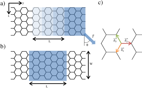
where represents the fermionic annihilation operator on site , is the hopping amplitude between nearest neighbor orbitals (in the unstrained lattice eV). The leading effect of uniaxial strain to the -band electrons arises through the modification of the carbon bond distances in equilibrium, [cf. Fig. 1(c)], according to , where is the plane displacement gradient tensor. Since we are interested in characterizing the effects on the quantum transport across non-strained-to-strained junctions, throughout this work we shall consider only the representative case of uniaxial and planar deformations. In this case the deformation gradient tensor can be exactly replaced by its symmetric decomposition, the small strain tensor: . In the coordinate system shown in in Fig. 1 the strain tensor reads Vitor M. Pereira et al. (2009)
| (2) |
where is the magnitude of the applied tension, is the orientation with respect to the x direction (see Fig. 1), and is the Poisson ratio. The strain-induced changes in the three nearest neighbor vectors modify the value of the corresponding hopping amplitudes. Their dependence on the distance between neighboring orbitals is modeled to vary according to Vitor M. Pereira et al. (2009), with nm being the unstrained C-C bond length.
Of special significance are the cases of strain applied along the lattice zigzag (e.g., ) and armchair (e.g., ) directions Vitor M. Pereira et al. (2009). These two particular tension directions leave in both cases, and the nearest-neighbor distances are modified explicitly as
| (3a) | ||||
| (3b) | ||||
| and | ||||
| (3c) | ||||
| (3d) | ||||
Effects of strain in the spectrum of GNRs have been considered elsewhere by various authors. But these studies pertain mostly to situations where the entire nanostructure is under strain, and not the cases of strain barriers or junctions considered here. For example, it has been shown that strain does not qualitatively affect the intrinsic bandstructure of zigzag GNRs Poetschke et al. (2010); Li et al. (2010); Rasuli et al. (2010), whereas band structure calculations for AGNRs have shown a variable intrinsic gap with a sawtooth shape as a function of the applied strain. However, in the latter case the value of the intrinsic gap still scales with the inverse width of the ribbon, and hence becomes rapidly insignificant as the transverse dimension increases Sun et al. (2008). For calculational convenience, our analysis of the strain-induced transport gap generated by strain junctions will focus only on AGNRs, since these allow an analytical closed form for the propagating modes, which will be an important factor in the interpretation and analysis of the results. With reference to Fig. 1, ribbons of different width are identified by the number of atoms along one of the vertical zigzag chains, . Moreover, given that we are interested in following the evolution of the transport gap, the incoming (and outgoing) contact in the case of the junction (barrier) is always metallic. This means that we shall always choose , where is a positive integer. The width of the nanoribbon is denoted by , and is given by .
In the case of the unstrained-strained junction we define three regions in the infinite nanoribbon: an unstrained semi-infinite contact acting as a waveguide for the incident electrons, a strained semi-infinite contact acting as a waveguide for the transmitted electrons, and a central region of length acting as the scattering region (in this work we consider equal to the width of the GNR). The transition from the unstrained to the strained region is not abrupt. Instead, strain is smoothly incremented over a length (), which is a parameter that we can vary to assess the influence of the barrier smoothness on the conductance suppression at low densities. This is achieved with the following position dependent strain
| (4) |
where and mark the end of the unstrained left and the beginning of the right strained contact, respectively. For the study of the strain barrier, the infinite ribbon is likewise divided in three regions: two semi-infinite unstrained contacts and a strained central region of length . The strain magnitude is also smoothed at the interfaces of the central region with the contacts as described above.
The conductance of the graphene nanostructures is evaluated within the Landauer-Bttiker formalism, whereby , with . is the transmission function, and is obtained using the recursive lattice Green’s function technique Lewenkopf and Mucciolo (2013).
III Conductance of an unstrained-strained junction
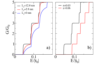
In order to understand how strain modifies the conductance of an AGNR and to compare it with the results obtained within the continuum approach based on the Dirac equation Vitor M. Pereira and Castro Neto (2009); Fogler et al. (2008b); Pellegrino et al. (2011) let us begin by describing the quantum transport features of the unstrained-strained junction. Fig. 2(a) shows how the conductance of an AGNR varies in general with the Fermi energy.
In view of the particle-hole symmetry of this problem, we show only the results for the conductance at positive energies. The value of the full transport gap is , where is the transport gap observed in plots such as the ones in Fig. 2, where only positive energies are shown. Throughout this work we shall refer to as the “transport gap”, being clear that it corresponds to half of . The specific parameters for this system are nm (ribbon width), (strain magnitude), (strain direction), and the onset of strain is smoothed over different lengths, . It is evident that, although the GNR is metallic in the absence of any strain, a transport gap develops, and its magnitude () is insensitive to . This means that, as far as the existence and magnitude of the transport gap at low energies is concerned, smoothing of the unstrained-strained interface has no effect (in the absence of disorder). The effect is therefore robust with respect to the degree of sharpness of the strain barrier, which is an important result since a real strain interface will never be abrupt, and strain will always develop incrementally. This is similar to what happens in a quantum point contact: when the width of the constriction is reduced gradually (adiabatically), the inter-subband mixing is reduced and the accuracy of the conductance quantization markedly improves de Jong and Beenakker (1997). One consequence of this is that, as seen in Fig. 2(a), the smoother the junction, the better defined the quantization plateaux become. In this sense smoother junctions are not only a necessity imposed by the actual elastic behavior of the system and experimental conditions, but also a desirable situation as far as observation of conductance quantization is concerned. Fig. 2(b) shows the typical behavior of the conductance of a smooth strain junction with increasing strain magnitude: the transport gap increases with (), but the conductance quantization remains unaffected, since plateaus are created at integer values of , with strain changing only the energies of the conductance steps.
It is crucial not to confuse the appearance of the transport gap with the finite sub-band spacing in a narrow nanoribbon. In other words, one could be tempted to think that, since the strained region is still a nanorribon of the same width but with the sub-bands slightly rearranged in energy, one would expect a small transport gap if the band arrangement in the strained region is such that it corresponds to an insulating nanoribbon. Even though this is true, it leads only to a small “intrinsic” gap scaling with , which is rapidly overshadowed by the strain-induced gap, whose scale is set by and is largely insensitive to the width .
In order to understand the behavior of the conductance reported in Fig. 2 it is instructive to review the band structure of the system and consider the characteristics of the incoming, reflected, and transmitted modes. The band dispersion of an AGNR with or (i.e., ) is given by , where
| (5) |
and . The transverse momentum is quantized as , where is the number of sites along a zigzag line in the transverse direction. The possible values of are identified by the mode index . For a given energy and transverse momentum there are two possible values of longitudinal momentum . All real values of for a given constitute a one-dimensional sub-band and, hence, the mode index also labels the sub-bands.
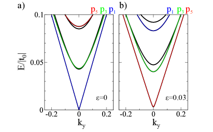
If we use to enumerate the conduction sub-bands in terms of increasing energy at we can then refer to their respective mode numbers as . In Fig. 3(a) we have an example of this notation: the first band above is the one corresponding to the mode , the second to the mode , and so on. In addition, since our unstrained ribbons are always metallic, we can use the fact that can be cast as , with a positive integer, and obtain the mode number of the lowest sub-band: Zheng et al. (2007). The usefulness of this labeling will now be made apparent with a particular example.
III.1 Transport gap and conductance quantization
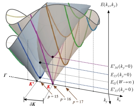
Consider Fig. 3 where the lowest sub-bands of a particular AGNR are plotted, with and without strain. Strain naturally modifies the electronic structure of the AGNR by (i) creating, in general, a small -dependent intrinsic gap ( in this particular case), and (ii) by reordering the relative position and energy of the sub-bands corresponding to the same mode index. In Fig. 3(a) we highlight the first, third, and fifth bands of the unstrained AGNR (whose mode indices are , and ), and show in Fig. 3(b) how the bands with the same mode numbers appear at different energies. It can be seen that the fifth band becomes the lowest energy band of the strained AGNR and the first band of the unstrained AGNR becomes the fourth. Fig. 4 illustrates this band rearrangement from a perhaps more instructive perspective. To understand why tracing the mode indices in the unstrained and strained regions is significant we should recall that, as stated above, the mode index defines the transverse momentum via . Since strain varies only along the longitudinal direction, the transverse momentum (or mode index) should be preserved across the interface. Additionally, since our geometry assumes an identical ribbon width in both strained and unstrained regions, the value of is identical on both. This means that an incoming mode will only propagate across the interface if that mode is “open” in the strained region, which is to say, if the corresponding band lies above . This is precisely what happens, and what determines the transport gap. Inspecting the energy eigenvalues at the point of the strained AGNR it is found that the value of the transport gap [, cf. Fig. 2] does not tally with an eigenenergy of the strained AGNR, but, instead, it coincides with an eigenenergy of the unstrained AGNR corresponding to the third band (). In other words, as is increased from zero the incoming electrons belong to mode up to ; this mode can only propagate in the strained region for ; hence the conductance is zero. The lowest common band to the unstrained and strained region is the one associated with the mode . Only when is increased past the minimum of this band can we have mode conservation, and this is what determines the transport gap.
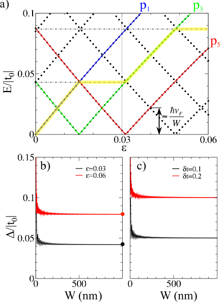
To delve more into this point we can follow the evolution of the eigenenergies at as a function of strain. The results are plotted in Fig. 5(a), where the evolution of the energies for modes , , and is highlighted. The variation of the eigenenergies is linear with strain, which is expected in connection with the illustration of Fig. 4: first, the displacement of the “enveloping Dirac cone” is linear in strain Ando (1991); Vitor M. Pereira and Castro Neto (2009); Castro Neto and et al. (2009), and, second, the energy is linear in the momentum close to the Dirac point.
As a result of the variation of the individual sub-bands with energy the intrinsic gap in the strained ribbon oscillates as strain increases, with an amplitude ; this is simply a consequence of the displacement of the Dirac cone induced by strain, and the constancy of the quantized transverse momenta Yang and Han (2000); Nagapriya et al. (2008); Lu and Guo (2010); Sun et al. (2008); Li et al. (2010). The transport gap , however, increases steadily with strain (except for a sawtooth modulation ). This can be appreciated with the aid of Fig. 5(a) that shows the minimum of each band as a function of strain. For example, following the vertical dashed line at the first eigenenergy is ; this value corresponds to mode . Since this mode is evanescent in the unstrained contact there is no transmission. The second eigenenergy is ; this value corresponds to mode . For this energy this mode is evanescent in the unstrained contact and consequently there is no transmission either. When the Fermi energy reaches the first horizontal dashed line, that is when the mode becomes propagating in the unstrained contact and starts to transmit, the transmission gap is reached since the modes are opened in both unstrained and strained contacts. Increasing the Fermi energy to the value of the eigenenergy corresponding to mode , there is no effect on the conductance because for this energy the mode is evanescent in the unstrained contact. Such a fine-grained analysis can be used to understand the position and width of the conductance plateaus in Fig. 2. Consider, for example, the very narrow plateau for in Fig. 2. It appears when the Fermi energy reaches the fourth eigenvalue () of the strained contact, and both modes (in the unstrained and strained regions) with are propagating and can transmit. Finally when the Fermi energy comes to the second horizontal dashed line the mode of the unstrained contact, finally is propagating and there is transmission in that mode. This also explains the origin of the shorter plateaus observed in the conductance of Fig. 2. Following the same procedure for the transmission gap is extracted form Fig. 5(a), it can be seen that the transmission gap is created when the modes labeled with are propagating in both contacts.
Simply generalizing this reasoning and procedure we can trace the dependence of the transport gap for any value of strain () and width (). Fig. 5(b) shows such results for and as a function of the width of the nanoribbon. It can be seen that the transport gap has strong oscillations for narrow ( nm) nanoribbons that rapidly die off with increasing , on account of the reduction of spatial confinement in the transverse direction. For wide junctions the transport gap eventually converges at the asymptotic values of and , for the particular values of strain considered in the figure for illustration. These results are in complete agreement with ones calculated using Dirac’s equation Pellegrino et al. (2011).
In addition, in order to make a direct comparison with the predictions for the transport gap predicted for the 2D graphene system under uniaxial strain, we calculated the transport gap of an unstrained-strained junction where only the hopping is modified in the strained contact. The values of were chosen to be equivalent to the values of obtained with and . In this ideal situation it is expected that Vitor M. Pereira and Castro Neto (2009) and, indeed, observing Fig. 5(c) it can be seen that this is the asymptotic value for wide nanoribbons.
III.2 Work function mismatch
To efficiently inject carriers from one material to another a good band alignment is required. The work function difference determines how the bands of different materials align when they are put in contact. It has been shown that the work function of graphene can be engineered through chemical doping Shi et al. (2010) or strain Choi et al. (2010); Peng et al. (2012). In particular, strain is known to increase or decrease the work function depending on whether the lattice is, respectively, strained or compressed. Consequently, different work functions in the strained and unstrained regions lead to band misalignment and this appears to require a reformulation of the model and calculations presented in the previous section. The band mismatch created by homogeneous strain can be regarded as an effective scalar potential Choi et al. (2010) relating the Fermi energies in the unstrained and strained region as , where () is the work function in the unstrained (strained) region. For AGNR it has been found that the work function increases linearly with uniaxial tensile strain up to 12 %, regardless the width of the nanoribbon Peng et al. (2012), and with a magnitude that can depend on the details of edge passivation. Since we are interested in the general consequences of a work function mismatch to the transport gap and conductance quantization, without compromising this generality we extracted eV and eV. These values correspond to the mismatch predicted in Ref. Peng et al., 2012 for hydrogen-passivated edges. With these parameters, the Fermi energy in the strained region, , can be written in terms of its unstrained counterpart, , and strain magnitude, , as
| (6) |
According to this, the effect of the strain-induced work function mismatch can be modeled by adding a strain-dependent on-site energy of to the sites in the strained region. The addition of this effective scalar potential does not affect the methods used in the previous section since transverse momentum conservation is still valid (the scalar potential is a function of strain, and this varies only along the longitudinal direction). We therefore used this approach to model and investigate the effects of work function mismatch. Since the strain variation is smoothed according to Eq. (4), the effective local potential will vary smoothly as well.
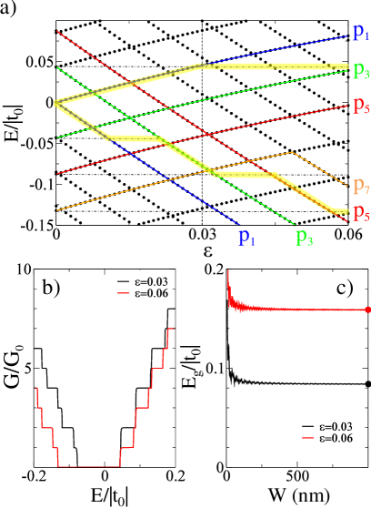
The effect of incorporating explicitly this work function mismatch in our conductance calculations is a downwards displacement of the eigenenergies in the strained region which, consequently, modifies the quantization signatures in the conductance trace, as well as the transmission gap. Since the conductance trace is no longer particle-hole symmetric (Fig. 6b), the transport gap is now determined by , which requires the explicit calculation of the transmission threshold at positive and negative energies, . For example, resorting to Fig. 6a that shows the evolution of the different modes with strain, we see that and , leading to a transport gap that is larger than the value obtained without work function mismatch. A larger transmission gap is also observed for (). In this case, the asymmetry induced by the local potential has the consequence that the modes responsible for the gap have changed, and is determined by mode from the positive energy branch, while is defined by mode from the negative branch. These considerations are confirmed by a direct calculation of the conductance, which is shown in Fig. 6b for these two particular values of strain (compare with Fig. 2b). The width dependence of the gap is shown in Fig. 6c. The asymptotic values for the full gap of and at, respectively, and , are seen to be equal to the full gaps obtained without work function mismatch (see Fig. 2c). This is highlighted by the dots located on the right vertical axis, which mark the positions and , where are the ones calculated in Fig. 2c.
The main message from here is that the work function mismatch displaces the center of the gap from to , but its magnitude remains unchanged relative to the case where work function mismatch is disregarded. This is a direct consequence of the linear spectrum of graphene which causes the strain-induced transport gap in the 2D limit to be independent of a uniform, but different, potential energy in the two regions. Moreover, the analysis of the mode evolution with strain from in Fig. 6a shows that the finite transport gap is still a consequence of the conservation of mode index (transverse momentum), and that the gap is determined by the lowest energy modes that are simultaneously “open” in the strained and unstrained regions. Finally, since we are ultimately interested in the behavior of the transport gap as a function of strain, these facts allow us to concentrate only on strain junctions where the explicit work function mismatch is ignored without losing generality as far as the magnitude and strain-dependence of the gap is concerned. In the remainder of this paper we therefore will not consider explicitly the work function mismatch.
III.3 Mode mixing
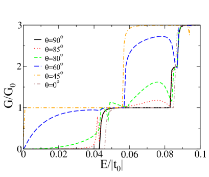
When the strain is not in the transverse or longitudinal directions (), Eq. (5) is no longer valid to calculate the dispersion relation, consequently the values of the quantized transverse momentum in the strained contact will differ form the values of the quantized transverse momentum in the unstrained contact. This will lead to mode mixing, even for a smooth junction or a junction without any kind of disorder. An electron incident upon the junction in a given mode will be mixed with a number of modes of the strained contact with similar transverse momentum and symmetry of the wave function Li et al. (2008); Wang et al. (2008) , as a consequence the transport gap will be reduced or disappears since its existence was due to the matching of the lowest energy propagating modes. Mode mixing will be small while the angle does not deviate too much from ideal situations ( and ), but this effect will reduce the value of the transport gap, as can be seen in Fig. 7 where the conductance of a strained junction of nm with is plotted for different angles of the applied strain. For we obtained a transport gap , and for we have . When the band structure is calculated for the strained AGNR, using the latter values, it can be corroborated that, in fact, there exists a transport gap since there are lower energy propagating modes that are not transmitting. For one sees an apparent transport gap , but it is only apparent because when the band structure is calculated this value corresponds to the lowest energy propagating mode and, hence we are observing the intrinsic gap, not a transport gap. When there is no transport or intrinsic gap. Observing Fig. 7 it is clear that any amount of mode mixing destroys the conductance quantization: some lineshapes of the conductance at higher energies can be traced back in the band structure of the strained contact. However for low energies the effect is completely due to the degree of mode mixing induced by angle of the applied strain.
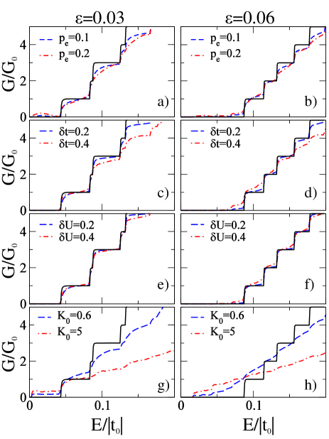
Another way to induce mode mixing is by adding disorder to the problem. To be specific, we consider the effect of adding disorder in a region of length between the perfect unstrained and strained contacts. Four disorder models were analyzed: (i) edge disorder, (ii) hopping disorder, (iii) short range bulk disorder, and (iv) long range bulk disorder. Edge disorder was implemented by removing sites from the outermost row of carbon atoms with a probability . In the hopping disorder model every hopping at the disordered region was modified according to , where is uniformly distributed in the interval . The short-range bulk disorder was modeled via a random on-site energy , where is a random number uniformly distributed over . Finally, long range bulk disorder was generated by randomly distributing impurities, each modeled by a Gaussian function of width , and with an amplitude selected from the uniform distribution . These impurities cause a modification of the on-site energy given by
| (7) |
and its strength is quantified with the dimensionless parameter , which in the dilute limit can be expressed as , where is the impurity density and is the lattice constant. Our strategy was to introduce a small amount of disorder to see how, for a given strain magnitude , the transport gap and the conductance were modified. The result is shown in Fig. 8, where we show the conductance averaged over 100 disorder realizations for each model and for two values of strain (left column) and (right column). Focusing on the transport gap, it can be seen that it is more strongly affected by edge and long-range disorder, its suppression being largely insensitive to the disorder strength in both situations. On the one hand, edge defects will induce strong back-scattering, particularly in low energy modes of the unstrained contact Mucciolo et al. (2009); Evaldsson et al. (2008); Li and Lu (2008); Zârbo and Nikoli´c (2007) which are just the modes reflected at the clean unstrained-strained junction. This back-scattering leads to mixing with the propagating modes below in the strained contact and, consequently, the transmission gap disappears. This effect is reduced in wider junctions (not shown), as well as in unstrained AGNR Mucciolo et al. (2009); Evaldsson et al. (2008). On-site long range disorder, on the other hand, will lead electron-hole puddles that strongly impact the low energy states Martin et al. (2008). This again will introduce mode mixing between the low energy modes of the unstrained contact with the low energy propagating modes below in the strained contact. Turning our attention now to the other two types of disorder — hopping in Fig. 8(c,d) and short range in Fig. 8(e,f) — one sees that mode mixing is moderate since the transport gap is only reduced, and the conductance quantization is still preserved to a very good degree Klos et al. (2009); Lherbier et al. (2008). Comparing the left and right panels of Fig. 8 one can see that the same amount of disorder washes out more efficiently the conductance features of the junction under the highest strain. This can be explained as arising from the fact that the larger the strain the more high energy modes of the unstrained contact become low energy propagating modes of the strained contact, as shown in Fig. 5(a). Therefore, in the energy range under consideration here, these modes can only by conducting because of the mode mixing.
IV Conductance of a disordered strained barrier
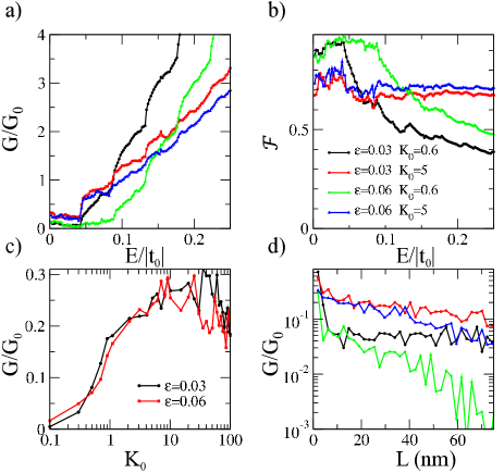
We now focus on the conductance of a disordered strain barrier. As defined earlier, this system consists of a strained region () of length between two perfect unstrained semi-infinite contacts (as illustrated in Fig. 1(b). In the absence of disorder and when the strain barrier is smooth the resulting conductance is exactly the same to that observed in the unstrained-strained junction.
This is expected because electron transmission can only occur when a given mode is opened in the three regions. Left and right contacts are exactly the same, and so the same mode will be accessible at the same energy in both contacts. In this case the reasoning of Fig. 5(a) can be repeated resulting in the same quantum conductance. The situation is analogous to the quantum point contact example: the quantization of the conductance is given by the narrower constriction.
Since we established above that on-site long-range disorder is the most efficient mode mixer, this is the only disorder model that we report on now. The resulting conductance averaged over 100 disorder realizations is presented in Fig. 9(a). There is no transport gap in the average conductance because of the relatively strong mode mixing in the strained disordered barrier (and there is no intrinsic gap in the contacts either). For low levels of disorder, , it is evident that mode mixing is lower since the lineshape of average conductance bears some resemblance to that of the unstrained-strained junction. It is even possible to observe the appearance of the small plateaus that were discussed above. It can also be concluded that larger strain transmits fewer modes (the conductance for a given energy is lower), and that the value of the conductance is small () in the energy range that corresponds to and of the unstrained-strained junction. When the disorder strength increases () there is no appreciable difference between the average conductance with and , and, in fact, the overall features of the conductance traces are no different from the conductance of a disordered unstrained barrier Mucciolo et al. (2009); Ihnatsenka and Kirczenow (2009) (but still, there is an increase of the average conductance, and the clear definition of the first two plateaus with values and ).
Shot noise is quantified by the dimensionless Fano factor , in particular it is a quantity that reveals information about the transport dynamics in the device. , where is the transmission probability of mode Blanter and Büttiker (2000); de Jong and Beenakker (1997). In the eigenmode representation the device can be seen as a parallel circuit of independent transmission modes, to access this representation in graphene – without using the analytic expression for metallic contacts Ferry and M. (1997); Robinson and Schomerus (2007); Lewenkopf et al. (2008); Dragomirova et al. (2009) – it is necessary a numerical method Ando (1991); Khomyakov et al. (2005); Sørensen et al. (2009). Fig. 9(b) shows the average Fano factor, using the same values of the average conductance of Fig. 9(a). For low disorder () and energies in the range of the Fano factor, , indicates a tunnel barrier behavior this is , as can be expected since there is no mode matching for that energy range. For the same energy range it is seen that the Fano factor oscillates, a clear indication that mode mixing is the main mechanism for the conductance enhancement. For higher energies than , the Fano factor begins to decay, that because of the mode matching between propagating modes in the contacts and in the strained barrier. For there is no qualitative differences between the Fano factor for different values of strain, disorder enhances the mode mixing and the transmission is increased (Fano factor is smaller), especially in the energy range of the first two plateaus of the average conductance in Fig. 9(a), as can be seen in the higher oscillations of Fano factor in that energy range. For higher energies the oscillations are damped and the Fano factor saturates. We followed the evolution of Fano factor for higher values of disorder up to (not showed) finding no significant changes in the lineshape and values of the average Fano factor.
Looking more closely the effect of disorder on the conductance and its relation with strain, especially in the energy range of , we fixed the Fermi energy at and increase the impurity density () in the strained barrier. After averaging over 100 realizations the average conductance is plotted in Fig. 9(c), it can be seen that the effect of strain is completely washed out by disorder, there is no appreciable differences between the curves with and . With the increase of the conductance is enhanced from for low disorder to in the intermediate disorder regime. We switch now to examine the effect of length of the strained barrier in the conductance, again we set the Fermi energy to and averaging over 500 disorder realization, the resulting conductance is plotted in Fig. 9(d). It is observed that the average conductance decreases exponentially with the length, for all disorder strength and applied strain. For it could be said that the localization length is roughly the same and that there are no appreciable differences in the lineshape and values of the average conductance for different values of strain. For the localization length is shorter for the higher strain value, this effect will be appreciated in lower conductance values for larger barriers, however there is no the formation of a transport gap.
V Summary
The electronic transport across strained junctions and barriers in a graphene nanorribon has been studied in the framework of Landauer and Büttiker, implemented using non-equilibrium Green’s functions. A clear strain-dependent transport gap appears for strain applied along the zigzag and armchair directions of non-disordered strain junctions and barriers. The transport gap is a result of the perfect matching between the propagating modes in both regions. A different angle of applied strain or disorder induces mode mixing, which tends to degrade the gap as well as the conductance quantization, both signatures of the electronic transport across a strained region. For Fermi energies in the energy range of the transport gap, the presence of unmatched propagating modes in the strained region means that they become active in the presence of disorder, leading to a conductance plateau that is sustained for a broad range of disorder strength. The conductance in this plateau decays exponentially indicating that strain induces localization in the low energy single channel regime Yamamoto et al. (2009).
We have shown results for disordered square junctions and barriers with nm. However, our results can be easily extrapolated to junctions and barriers of different aspect ratios. For larger disordered regions the number of scattering centers grows, the conductance decays and the quantization plateaus are destroyed for energies higher than the transport gap of the clean junction. For energies below the transport gap the conductance is enhanced leading to a broad plateau whose conductance value can be smaller that . Although not shown explicitly here, this was observed by direct calculations in junctions and barriers with nm , nm, and nm, as well as different aspect ratios.
Our results complement the existing calculations based on the 2D electronic dispersion that predict a strain-dependent transport gap at low densities, and lend support to the idea that this gap is robust against strain inhomogeneity, barrier smoothness and some degree of electronic disorder.
Acknowledgements.
This work was supported by the NRF-CRP award “Novel 2D materials with tailored properties: beyond graphene” (R-144-000-295-281).References
- Schwierz (2010) F. Schwierz, Nat Nano 5, 487 (2010).
- Novoselov and Castro Neto (2012) K. S. Novoselov and A. H. Castro Neto, Physica Scripta 2012, 014006 (2012).
- Cadelano et al. (2009) E. Cadelano, P. L. Palla, S. Giordano, and L. Colombo, Phys. Rev. Lett. 102, 235502 (2009).
- Lee et al. (2008) C. Lee, X. Wei, J. W. Kysar, and J. Hone, Science 321, 385 (2008).
- Rogers et al. (2010) J. A. Rogers, T. Someya, and Y. Huang, Science 327, 1603 (2010).
- Levy and et al. (2010) N. Levy and et al., Science 329, 544 (2010).
- Lu et al. (2012) J. Lu, A. H. Castro Neto, and K. P. Loh, Nature Commun. 3, 823 (2012).
- Tomori et al. (2011) H. Tomori, A. Kanda, H. Goto, Y. Ootuka, K. Tsukagoshi, S. Moriyama, E. Watanabe, and D. Tsuya, Applied Physics Express 4, 075102 (2011).
- Vitor M. Pereira and Castro Neto (2009) Vitor M. Pereira and A. H. Castro Neto, Phys. Rev. Lett. 103, 046801 (2009).
- Vitor M. Pereira et al. (2009) Vitor M. Pereira, A. H. Castro Neto, and N. M. R. Peres, Phys. Rev. B 80, 045401 (2009).
- Guinea et al. (2010) F. Guinea, M. I. Katsnelson, and A. K. Geim, Nature Physics 6, 30 (2010).
- Fogler et al. (2010) M. M. Fogler, A. H. Castro Neto, and F. Guinea, Phys. Rev. B 81, 161408 (2010).
- Kim et al. (2011) K. Kim, Z. Lee, B. D. Malone, K. T. Chan, B. Alemán, W. Regan, W. Gannett, M. F. Crommie, M. L. Cohen, and A. Zettl, Phys. Rev. B 83, 245433 (2011).
- Rainis et al. (2011) D. Rainis, F. Taddei, M. Polini, G. León, F. Guinea, and V. I. Fal’ko, Phys. Rev. B 83, 165403 (2011).
- Kane and Mele (1997) C. L. Kane and E. J. Mele, Phys. Rev. Lett. 78, 1932 (1997).
- Suzuura and Ando (2002) H. Suzuura and T. Ando, Phys. Rev. B 65, 235412 (2002).
- Castro Neto and et al. (2009) A. H. Castro Neto and et al., Rev. Mod. Phys. 81, 109 (2009).
- Qi et al. (2013) Z. Qi, D. A. Bahamon, Vitor M. Pereira, H. S. Park, D. K. Campbell, and A. H. Castro Neto, Nano Letters 13, 2692 (2013).
- Vitor M. Pereira and et al. (2010) Vitor M. Pereira and et al., Eur. Phys. Lett. p. 67001 (2010).
- Pellegrino et al. (2010) F. M. D. Pellegrino, G. G. N. Angilella, and R. Pucci, Phys. Rev. B 81, 035411 (2010).
- Bunch et al. (2007) J. S. Bunch, A. M. van der Zande, S. S. Verbridge, I. W. Frank, D. M. Tanenbaum, J. M. Parpia, H. G. Craighead, and P. L. McEuen, Science 315, 490 (2007).
- Ong and Reed (2012) M. T. Ong and E. J. Reed, ACS Nano 6, 1387 (2012).
- Low and Guinea (2010) T. Low and F. Guinea, Nano Letters 10, 3551–3554 (2010).
- Fogler et al. (2008a) M. M. Fogler, F. Guinea, and M. I. Katsnelson, Phys. Rev. Lett. 101, 226804 (2008a).
- Wu et al. (2011) Z. Wu, F. Zhai, F. M. Peeters, H. Q. Xu, and K. Chang, Phys. Rev. Lett. 106, 176802 (2011).
- Masir et al. (2009) M. R. Masir, P. Vasilopoulos, and F. M. Peeters, New Journal of Physics 11, 095009 (2009).
- Liu et al. (2010) Z. Liu, J. Wu, W. Duan, M. G. Lagally, and F. Liu, Phys. Rev. Lett. 105, 016802 (2010).
- Hoyt et al. (2002) J. Hoyt, H. Nayfeh, S. Eguchi, I. Aberg, G. Xia, T. Drake, E. Fitzgerald, and D. Antoniadis, in Electron Devices Meeting, 2002. IEDM ’02. International (2002), pp. 23–26.
- Bao et al. (2009) W. Bao, F. Miao, Z. Chen, H. Zhang, W. Jang, C. Dames, and C. Lau, Nature Nanotechnology 4, 562 (2009), cited By (since 1996)267.
- Gattenlöhner et al. (2010) S. Gattenlöhner, W. Belzig, and M. Titov, Phys. Rev. B 82, 155417 (2010).
- Cheianov and Fal’ko (2006) V. V. Cheianov and V. I. Fal’ko, Phys. Rev. B 74, 041403 (2006).
- Kosynkin et al. (2009) D. V. Kosynkin, A. L. Higginbotham, A. Sinitskii, J. R. Lomeda, A. Dimiev, B. K. Price, and J. M. Tour, Nature 458, 872 (2009).
- Cai et al. (2010) J. Cai, P. Ruffieux, R. Jaafar, M. Bieri, T. Braun, S. Blankenburg, M. Muoth, A. P. Seitsonen, M. Saleh, X. Feng, et al., Nature 466, 470 (2010).
- et al. (2012) H. H. et al., Scientific Reports 2, 983 (2012).
- Poetschke et al. (2010) M. Poetschke, C. G. Rocha, L. E. F. Foa Torres, S. Roche, and G. Cuniberti, Phys. Rev. B 81, 193404 (2010).
- Li et al. (2010) Y. Li, X. Jiang, Z. Liu, and Z. Liu, Nano Research 3, 545 (2010).
- Rasuli et al. (2010) R. Rasuli, H. Rafii-Tabar, and A. I. zad, Phys. Rev. B 81, 125409 (2010).
- Sun et al. (2008) L. Sun, Q. Li, H. Ren, H. Su, Q. W. Shi, and J. Yang, J. Chem. Phys. 129, 074704 (2008).
- Mohiuddin et al. (2009) T. M. G. Mohiuddin, A. Lombardo, R. R. Nair, A. Bonetti, G. Savini, R. Jalil, N. Bonini, D. M. Basko, C. Galiotis, N. Marzari, et al., Phys. Rev. B 79, 205433 (2009).
- Ferralis et al. (2008) N. Ferralis, R. Maboudian, and C. Carraro, Phys. Rev. Lett. 101, 156801 (2008).
- Ni et al. (2008) Z. H. Ni, W. Chen, X. F. Fan, J. L. Kuo, T. Yu, A. T. S. Wee, and Z. X. Shen, Phys. Rev. B 77, 115416 (2008).
- Yan et al. (2012) H. Yan, Y. Sun, L. He, J.-C. Nie, and M. H. W. Chan, Phys. Rev. B 85, 035422 (2012).
- et al. (2011) N.-C. Y. et al., Surf. Sci. 605, 1649 (2011).
- Lewenkopf and Mucciolo (2013) C. Lewenkopf and E. Mucciolo, Journal of Computational Electronics 12, 203 (2013).
- Fogler et al. (2008b) M. M. Fogler, F. Guinea, and M. I. Katsnelson, Phys. Rev. Lett. 101, 226804 (2008b).
- Pellegrino et al. (2011) F. M. D. Pellegrino, G. G. N. Angilella, and R. Pucci, Phys. Rev. B 84, 195404 (2011).
- de Jong and Beenakker (1997) M. J. M. de Jong and C. W. J. Beenakker, in Mesoscopic Electron Transport, edited by L. P. Sohn, L. L.and Kouwenhoven and G. Schn (Kluwer Academic Publishing, 1997), pp. 225–258.
- Zheng et al. (2007) H. Zheng, Z. F. Wang, T. Luo, Q. W. Shi, and J. Chen, Phys. Rev. B 75, 165414 (2007).
- Ando (1991) T. Ando, Phys. Rev. B 44, 8017 (1991).
- Yang and Han (2000) L. Yang and J. Han, Phys. Rev. Lett. 85, 154 (2000).
- Nagapriya et al. (2008) K. S. Nagapriya, S. Berber, T. Cohen-Karni, L. Segev, O. Srur-Lavi, D. Tománek, and E. Joselevich, Phys. Rev. B 78, 165417 (2008).
- Lu and Guo (2010) Y. Lu and J. Guo, Nano Research 3, 189 (2010).
- Shi et al. (2010) Y. Shi, K. K. Kim, A. Reina, M. Hofmann, L.-J. Li, and J. Kong, ACS Nano 4, 2689 (2010), pMID: 20433163.
- Choi et al. (2010) S.-M. Choi, S.-H. Jhi, and Y.-W. Son, Phys. Rev. B 81, 081407 (2010).
- Peng et al. (2012) X. Peng, F. Tang, and A. Copple, Journal of Physics: Condensed Matter 24, 075501 (2012).
- Li et al. (2008) Z. Li, H. Qian, J. Wu, B.-L. Gu, and W. Duan, Phys. Rev. Lett. 100, 206802 (2008).
- Wang et al. (2008) Z. F. Wang, Q. Li, Q. W. Shi, X. Wang, J. Yang, J. G. Hou, and J. Chen, Applied Physics Letters 92, 133114 (pages 3) (2008).
- Mucciolo et al. (2009) E. R. Mucciolo, A. H. Castro Neto, and C. H. Lewenkopf, Phys. Rev. B 79, 075407 (2009).
- Evaldsson et al. (2008) M. Evaldsson, I. V. Zozoulenko, H. Xu, and T. Heinzel, Phys. Rev. B 78, 161407 (2008).
- Li and Lu (2008) T. C. Li and S.-P. Lu, Phys. Rev. B 77, 085408 (2008).
- Zârbo and Nikoli´c (2007) L. P. Zârbo and B. K. Nikoli´c, EPL (Europhysics Letters) 80, 47001 (2007).
- Martin et al. (2008) J. Martin, N. Akerman, G. Ulbricht, T. Lohmann, J. H. Smet, K. von Klitzing, and A. Yacoby, Nat Phys 4, 144 (2008).
- Klos et al. (2009) J. W. Klos, A. A. Shylau, I. V. Zozoulenko, H. Xu, and T. Heinzel, Phys. Rev. B 80, 245432 (2009).
- Lherbier et al. (2008) A. Lherbier, B. Biel, Y.-M. Niquet, and S. Roche, Phys. Rev. Lett. 100, 036803 (2008).
- Ihnatsenka and Kirczenow (2009) S. Ihnatsenka and G. Kirczenow, Phys. Rev. B 80, 201407 (2009).
- Blanter and Büttiker (2000) Y. Blanter and M. Büttiker, Physics Reports 336, 1 (2000).
- Ferry and M. (1997) D. K. Ferry and G. S. M., Transport in Nanostructures (Cambridge University Press., UPH, Shaftesbury Road, Cambridge, CB2 8BS, United Kingdom, 1997).
- Robinson and Schomerus (2007) J. P. Robinson and H. Schomerus, Phys. Rev. B 76, 115430 (2007).
- Lewenkopf et al. (2008) C. H. Lewenkopf, E. R. Mucciolo, and A. H. Castro Neto, Phys. Rev. B 77, 081410 (2008).
- Dragomirova et al. (2009) R. L. Dragomirova, D. A. Areshkin, and B. K. Nikolić, Phys. Rev. B 79, 241401 (2009).
- Khomyakov et al. (2005) P. A. Khomyakov, G. Brocks, V. Karpan, M. Zwierzycki, and P. J. Kelly, Phys. Rev. B 72, 035450 (2005).
- Sørensen et al. (2009) H. H. B. Sørensen, P. C. Hansen, D. E. Petersen, S. Skelboe, and K. Stokbro, Phys. Rev. B 79, 205322 (2009).
- Yamamoto et al. (2009) M. Yamamoto, Y. Takane, and K. Wakabayashi, Phys. Rev. B 79, 125421 (2009).