∎
33email: bnikolic@udel.edu
Negative differential resistance in graphene-nanoribbon–carbon-nanotube crossbars: A first-principles multiterminal quantum transport study
Abstract
We simulate quantum transport between a graphene nanoribbon (GNR) and a single-walled carbon nanotube (CNT) where electrons traverse vacuum gap between them. The GNR covers CNT over a nanoscale region while their relative rotation is 90∘, thereby forming a four-terminal crossbar where the bias voltage is applied between CNT and GNR terminals. The CNT and GNR are chosen as either semiconducting (s) or metallic (m) based on whether their two-terminal conductance exhibits a gap as a function of the Fermi energy or not, respectively. We find nonlinear current-voltage (I–V) characteristics in all three investigated devices—mGNR-sCNT, sGNR-sCNT and mGNR-mCNT crossbars—which are asymmetric with respect to changing the bias voltage from positive to negative. Furthermore, the I–V characteristics of mGNR-sCNT crossbar exhibits negative differential resistance (NDR) with low onset voltage V and peak-to-valley current ratio . The overlap region of the crossbars contains only carbon and hydrogen atoms which paves the way for nanoelectronic devices ultrascaled well below the smallest horizontal length scale envisioned by the international technology roadmap for semiconductors. Our analysis is based on the nonequilibrium Green function formalism combined with density functional theory (NEGF-DFT), where we also provide an overview of recent extensions of NEGF-DFT framework (originally developed for two-terminal devices) to multiterminal devices.
Keywords:
crossed nanowires negative differential resistance graphene nanoribbons carbon nanotubes first-principles quantum transportpacs:
73.63.Fg 72.80.Vp 85.35.-p1 Introduction
The discovery of a wonder material graphene—as the first one-atom-thick crystal whose honeycomb lattice of carbon atoms imposes gapless, massless and chiral Dirac spectrum on its low-energy quasiparticles—has swiftly ignited intense experimental and theoretical studies of its unusual electronic transport properties Geim2009 . The “first wave” of such studies DasSarma2011 has been largely focused on explaining conductivity measurements at small bias voltage applied to large-area graphene samples as a function of carrier density, temperature and magnetic field. These studies have typically relied on simplistic model Hamiltonians.
What could be termed the “second wave” of studies of electronic transport in graphene has been largely focused on confined structures (such as nanoribbons and nanoflakes Botello-Mendez2011 ; Habib2012 ), functional graphene-based devices (such as transistors Schwierz2010 and pn junctions Young2011 ; Nguyen2013 ) and novel state variables (such as pseudospin in mono- and bi-layer graphene, real electronic spin, wavefunction phase Habib2012 , and properties of correlated many-body quantum states like exciton condensates Pesin2012 ). The greatest roadblock to continued scaling of conventional silicon electronic for digital applications is the power dissipated in various leakage mechanisms Keyes2005 . The quantum coherent transport regime and novel state variables in graphene offer a prospect for revolutionary device designs that go beyond traditional (silicon or carbon) field-effect transistors (FETs) based on classical physics. For example, exploiting them would make possible to switch current off without utilizing energy barrier of traditional FETs, thereby evading thermal limitations in the subthreshold regime Schwierz2010 .
Concurrently, recent advances in nanofabrication and surface science have pushed the attention towards more complex structures of “second generation graphene” Agnoli2013 , such as chemically modified graphene (i.e., graphene sheets where carbon atoms are replaced by other atoms or entire functional groups) or three-dimensional systems based on the assembly of graphene sheets (where they form interconnected networks or highly complex nanoobjects like hollow nanospheres, crumpled paper, and capsules). Another route involves creating hybrid nanostructures which combine flat graphene sheets with previously amply explored carbon nanotubes (CNTs) that can be viewed as rolled up sheets of graphene.
For example, the recent experiment Jiao2010 has created aligned graphene nanoribbon (GNR) arrays by unzipping of aligned single-walled and few-walled CNT arrays. Then, novel GNR-GNR and GNR-CNT crossbars were fabricated by transferring GNR arrays across GNR and CNT arrays, respectively. The production of such ordered architectures may allow for large scale integration of GNRs into nanoelectronics or optoelectronics. We note that the crossbar geometry has been explored over the past decade using typically semiconductor nanowires, such as those made of Si or GaN Lu2008 , as well as crossed CNTs Fuhrer2000 . Such motif offers high device density and efficient interconnects between individual devices and functional device arrays, while a reconfigurable crossbar structure allows for effective incorporation of defect-tolerant computing schemes Lu2008 .
In contrast to vigorous experimental studies of nanowire crossbars, little theoretical guidance in designing such nanoelectronic devices has been offered by quantum transport simulations. For example, recent studies of GNR-GNR crossbars have utilized semi-empirical tight-binding model Botello-Mendez2011 or extended Hückel model Habib2012 with their parameters fitted to density functional theory (DFT) calculations. These models are then coupled to nonequilibrium Green function (NEGF) formalism Stefanucci2013 to compute the zero-bias transmission function Botello-Mendez2011 , or even current at finite bias voltage Habib2012 . While such approaches can capture charge transfer between different atomic species in equilibrium, they fail to capture more complicated charge redistribution due to nonequilibrium steady transport state driven by the applied bias voltage. On the other hand, the self-consistency of nonequilibrium charge and the corresponding electrostatic (Hartree) potential are indispensable in order to satisfy the gauge-invariant condition according to which I–V characteristics should not change when electric potential everywhere is shifted by a constant amount Christen1996 .
The state-of-the-art approach that has emerged over the past decade and which can capture both charge transfer in equilibrium and charge redistribution in nonequilibrium is NEGF-DFT Sanvito2011 ; Areshkin2010 ; Taylor2001 ; Brandbyge2002 ; Palacios2002 ; Rocha2006 ; Stokbro2008 . However, virtually all widely used NEGF-DFT scientific codes, such as commercial ATK atk and NANODCAL nanodcal or open source TranSIESTA siesta , SMEAGOL smeagol , ALACANT alacant , and GPAW gpaw can handle only devices with two electrodes (GPAW can also simulate multiterminal quantum transport but only in the linear-response regime Chen2012b ).
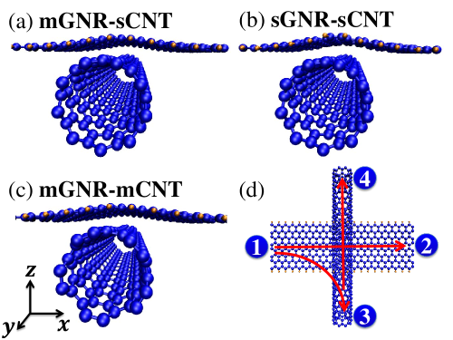
Here we overview the recent extension Saha2009 ; Saha2010a ; Saha2010 ; Saha2011 of NEGF-DFT framework to treat nanojunctions whose active region is attached to more than two electrodes, and then apply it to GNR-CNT crossbars illustrated in Fig. 1. The primary motivation to investigate four-terminal GNR-CNT crossbars comes from already fabricated structures of this type in Ref. Jiao2010 , so that our study could guide selection of specific GNR and CNT elements and their mutual orientation in future efforts to exploit GNR-CNT crossbars for applications in carbon-based nanoelectronics.
Our principal result—I–V curves plotted in Fig. 4—offers prediction of negative differential resistance (NDR) Ferry2009 in mGNR-sCNT crossbars. That is, as the source-drain bias voltage increases, current in Fig. 4(a) reaches a local maximum and then decrease to a valley region before rising again. The conventional NDR-based devices, used in a variety of applications (such as, frequency multipliers, memory, fast switches, and high frequency oscillators up to the THz range), are based on quantum tunneling or intervalley carrier transfer in two-terminal devices like Esaki or Gunn diodes. The advent of graphene has also brought theoretical proposals for NDR in two-terminal GNRs Ren2009 ; Nguyen2013 , as well as experimental demonstration Wu2012 of three-terminal large-area graphene where the gate electrode controls the current density and the onset of NDR based on ambipolar transport rather than tunneling. The NDR predicted in Fig. 4(a), with low onset voltage V and peak-to-valley current ratio , emerges in an ultrascaled geometry containing only carbon atoms in the overlap region.
The paper is organized as follows. In Sec. 2, we discuss details of atomistic structure of three selected GNR-CNT crossbars shown in Fig. 1. Section 3 overviews construction of the nonequilibrium density matrix for multiterminal devices as the key quantity that has to be extended in NEGF-DFT framework. In Sec. 4, we discuss zero-bias transmission function between different terminals of GNR-CNT crossbar while current from GNR to CNT at finite bias voltage is discussed in Sec. 5. We conclude in Sec. 6.
2 Device setup for modeling of GNR-CNT crossbars
We denote graphene nanoribbons with zigzag edges ZGNRs, while AGNRs denotes nanoribbons with armchair edges. We recall that ZGNRs are labeled as -ZGNR when they are composed of zigzag chains of carbon atoms, and -AGNR denotes AGNRs composed of dimers of carbon atoms Son2006a . The single-walled CNTs are labeled by the chiral vector, , where and are integers and and are the real space unit vectors of the graphene sheet. The vector specifies the way the graphene sheet is wrapped.
In analogy with the experiments on CNT-CNT crossbars Fuhrer2000 , which have utilized combination of metallic and semiconducting CNTs, we select three different setups for GNR-CNT crossbars depicted in panels (a)–(c) of Fig. 1: (a) crossed metallic 8-ZGNR and semiconducting single-walled (9,0)-CNT; (b) crossed semiconducting 14-AGNR and semiconducting single-walled (9,0)-CNT; and (c) crossed metallic 8-ZGNR and single-walled metallic (5,5)-CNT. The diameter of (9,0)-CNT is nm, while nm for (5,5)-CNT. The width of 8-ZGNR is nm and the width of 14-AGNR is nm.
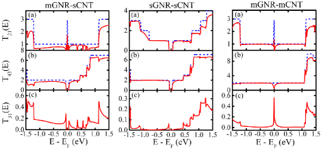
Simplistic tight-binding models predict that when is a multiple of , subbands will cross at the Fermi energy implying that CNT is metallic; otherwise, it is expected to be a semiconductor. The energy gap of semiconducting CNTs is inversely proportional to their diameter. Thus, -CNTs are expected to always be metallic, whereas -CNTs are expected to be metallic only when is a multiple of . However, experiments and DFT calculations with properly chosen exchange-correlation (XC) functional show that this is not always correct Matsuda2010 . For example, experiments Ouyang2001 have found eV for (9,0)-CNT, which is well-matched by the DFT calculations (using the B3LYP flavor of XC functional) eV Matsuda2010 . The transmission function plotted in Fig. 3 [see dashed line in subpanels (b) of mGNR-sCNT and sGNR-sCNT panels] for an infinite homogeneous (9,0)-CNT exhibits eV around the Fermi energy .
While simplistic tight-binding models predict that AGNRs are metallic for ( is a positive integer), DFT calculations show that all AGNRs have energy gap in their electronic subband structure due to transverse confinement Son2006a , which is eV in Fig. 3 [see dashed line in subpanel (a) of sGNR-sCNT panel] for the selected 14-AGNR used for the crossbar in Fig. 1(b).
Although ZGNRs are insulating at very low temperatures due to one-dimensional spin-polarized edge states coupled across the width of the nanoribbon, such unusual magnetic ordering and the corresponding band gap is easily destroyed above K Yazyev2008 ; Kunstmann2011 . Thus, they can be considered as good candidates for metallic electrodes and interconnects Areshkin2007a . In fact, the recent experiment Jia2009 has confirmed the flow of edge currents Chang2012 in metallic ZGNRs which were actually utilized to increase the heat dissipation around edge defects and, thereby, rearrange atomic structure locally until sharply defined zigzag edge is achieved.
The infinite GNR and CNT in our simulation are separated initially by a distance Å, where the overlap region consisting of 486, 480 or 458 carbon and hydrogen atoms [for panels (a)–(c) in Fig. 1, respectively] is structurally optimized using VASP simulation package Kresse1993 ; Kresse1996 ; Kresse1996a . Note that central region of the crossbars, for which NEGFs discussed in Sec. 3 are computed to obtain currents, includes the GNR-CNT overlap region + portion of the semi-infinite electrodes so that the total number of simulated atoms is 882, 888 or 838 for panels (a)–(c) in Fig. 1, respectively. The electron-core interactions are described by the projector augmented wave method Blochl1994 ; Kresse1999 , while we use Perdew-Burke-Ernzerhof (PBE) Perdew1996 parametrization of the generalized gradient approximation (GGA) for the XC functional. The cutoff energies for the plane wave basis set used to expand the Kohn-Sham orbitals are 400 eV for all calculations. A -point mesh within Monkhorst-Pack scheme is used for the Brillouin zone integration. This procedure ensures that Hellmann-Feynman forces acting on ions are less than . The final optimized atomic positions in Fig. 1 show how GNRs curve around CNT within their overlap region, as also observed in the atomic force microscope imaging of recently fabricated GNR-CNT crossbars Jiao2010 . After optimization, the spacing between GNRs and CNTs in Fig. 1(a)–(c) along the -axis (intersecting with tube axis) is Å.
For the study of near-equilibrium (i.e., linear-response) quantum transport in Sec. 4, we compute zero-bias transmission coefficients between different electrodes, labeled as in Fig. 1(d), which are kept at the same potential. For the study of I–V characteristics in nonequilibrium transport in Sec. 5, bias voltage is applied between GNR and CNT by shifting the electrode potentials by , , and .
3 NEGF-DFT methodology for multiterminal devices
The traditional CAD tools for electronic device simulations, based on classical drift-diffusion or semiclassical Boltzmann equation, are inapplicable to quasiballistic nanoscale active region attached to much larger reservoirs. This is exemplified by the crossbars in Fig. 1 which can be viewed as the nanoscale overlap region of GNR and CNT that is attached to four semi-infinite electrodes which terminate at infinity into macroscopic reservoirs. The proper description of such open quantum systems can be achieved using quantum master equations for the reduced density matrix of the active region Breuer2002 ; Timm2008 or the NEGF formalism Stefanucci2013 . The former is typically used when the active region is weakly coupled to the reservoirs (so that coupling between the active region and the electrodes is treated perturbatively Koller2010 ), while the latter is employed in the opposite limit.
The NEGF formalism Stefanucci2013 for steady-state transport operates with two central quantities, the retarded and the lesser Green functions , which describe the density of available quantum states and how electrons occupy those states, respectively. Its application to electronic transport often proceeds by combining Ferry2009 ; Datta1995 it with tight-binding (TB) Hamiltonians whose hopping parameters can be fitted using more microscopic theory Barraza-Lopez2013 . For example, proper description of quantum transport through GNRs with armchair or zigzag edges requires to employ TB models with either three orbitals per C atom and nearest-neighbor hopping Boykin2011 , or single orbital per C atom and third-nearest-neighbor hoppings Chang2012 .
However, at finite bias voltage Hamiltonian has to be recomputed self-consistently to capture the nonequilibrium charge redistribution. The NEGF-DFT framework can solve this problem, as long as the coupling between the active device region and the electrodes is strong enough to ensure transparent contact and diminish Coulomb blockade effects Koller2010 . The DFT part of this framework is employed using typical approximations (such as local density approximation, GGA, or B3LYP Fiolhais2003 ) for its XC functional. The sophisticated computational algorithms Sanvito2011 ; Areshkin2010 ; Taylor2001 ; Brandbyge2002 ; Stokbro2008 ; Rungger2008 developed to implement the NEGF-DFT framework can be encapsulated by the iterative self-consistent loop
| (1) |
The loop starts from the initial input electron density and then employs some standard DFT code Fiolhais2003 , typically in the basis set of finite-range orbitals for the valence electrons which allows for faster numerics and unambiguous partitioning of the system into the central region and the semi-infinite ideal electrodes. The DFT part of the calculation yields the single particle Kohn-Sham (KS) Hamiltonian
| (2) | |||||
| (3) |
Here is the DFT mean-field potential due to other electrons, which includes the Hartree potential , the XC potential and the external potential . The inversion of , represented in the some basis of local orbitals as the matrix of elements , yields the retarded Green function
| (4) |
The overlap matrix has elements . The non-Hermitian matrices are the retarded self-energies due to the “interaction” with the semi-infinite electrode whose electronic structure is assumed to be rigidly shifted by the applied voltage . The self-energies determine escape rates of electrons from the central region into the semi-infinite ideal electrodes, so that an open quantum system can be viewed as being described by the non-Hermitian Hamiltonian . The matrices account for the level broadening due to the coupling to the electrodes Stefanucci2013 .
Assuming the elastic transport regime (where electron-phonon, electron-electron and electron-spin scattering is neglected), can be expressed solely in terms of to determine the density matrix via
| (5) |
The matrix elements are the new electron density as the starting point of the next iteration. This procedure is repeated until the convergence criterion is reached, where is a suitably chosen tolerance parameter.
The NEGF post-processing of the result of the DFT loop expresses the current flowing into terminal of the device as
| (6) |
Here the transmission coefficients
| (7) |
are integrated over the energy window defined by the difference of the Fermi functions
| (8) |
of macroscopic reservoirs into which semi-infinite ideal electrodes terminate, where is the Fermi energy for the whole device in equilibrium.
The brute force integration in Eq. (5) directly along the real axis can hardly be accomplished due to sharp features (such as van Hove singularities in the density of states) in the integrand which make convergence with increasing number of energy mesh points virtually impossible. Instead, this expression has to be rewritten in the form more suitable for numerical implementation. Thus, the main difference between the usual two-terminal NEGF-DFT methodology Brandbyge2002 and the multiterminal Saha2009 ; Saha2010a ; Saha2010 ; Saha2011 one is in computational algorithms employed to construct the density matrix in Eq. (5), as well as in algorithms for solving the Poisson equation with boundary conditions imposed by the voltages applied to multiple electrodes. This ensures that transmission coefficients self-consistently depend on the voltages applied to the electrodes other than , through the inhomogeneous electrostatic (Hartree) potential acting on electrons within the central device region. The discussion of algorithms for the computation of the density matrix is made transparent by focusing on specific examples where we contrast two-terminal vs. multiterminal cases in Secs. 3.1 and 3.2, respectively. We also discuss how to solve the Poisson equation for four-terminal junction in Sec. 3.3.
Our MT-NEGF-DFT code Saha2009 ; Saha2010a ; Saha2010 ; Saha2011 , implementing equations discussed in Sec. 3.2, utilizes ultrasoft pseudopotentials and PBE Perdew1996 parametrization of GGA for the XC functional of DFT. The localized basis set for DFT calculations is constructed from atom-centered orbitals—six per C atom and four per H atom with atomic radius 8.0 Bohr for the devices shown in Fig. 1. These orbitals are optimized variationally for the electrodes and the central region separately while their electronic structure is obtained concurrently.
3.1 Two-terminal case
In the two-terminal case, the integration in Eq. (5) for the elastic transport regime is typically separated into apparent “equilibrium” and “nonequilibrium” terms as follows Brandbyge2002 . We first add and subtract the term to , to get after some rearrangements
| (9) |
Here we assume that semi-infinite electrode is connected to a macroscopic reservoir at the lower electrochemical potential . By substituting the following identity
| (10) |
into Eq. (9), we finally obtain
| (11) |
This allows us to rewrite Eq. (5) in the two-terminal case as the sum of two contributions
| (12) |
where . The first “equilibrium” term contains integrand which is analytic in the upper complex plane, so that it can be computed via the semicircular path combined with the path in the upper complex plane parallel to the real axis Areshkin2010 ; Brandbyge2002 . The lower energy limit EB is below the bottom valence-band edge. Because and are nonanalytic functions below and above the real axis, respectively, the integrand in the second “nonequilibrium” term111Note that conventionally used “equilibrium” and “nonequilibrium” terminology for the two terms is handy, but it is not exact since these two terms do not satisfy the gauge-invariant condition, as is the case of proper equilibrium and nonequilibrium density matrices discussed in Ref. Mahfouzi2013 . is nonanalytic function in the entire complex energy plane, so that integration Areshkin2010 ; Sanvito2011 has to be done directly along the real axis between the boundaries around and determined by the difference of the Fermi functions. The principal challenge for integration in the “nonequilibrium” term are sharp peaks in the integrand (due to, e.g., quasibound states or van Hove singularities at the subband edges in the density of state of the electrodes), which proliferate with increasing number of atoms in the central device region and which have to be handled by some version of adaptive mesh of energy points Sanvito2011 ; Areshkin2010 .
3.2 Multiterminal case
In the multiterminal case, we use similar manipulation as in Sec. 3.1 to rewrite Eq. (5) as
| (13) | |||||
Here energy EB is now chosen below the valence band of all the different electrodes. While in analogy to Sec. 3.1 electrode can be chosen as the one which is connected to the reservoir at the lowest electrochemical potential , in practice we recompute in Eq. (13) for all possible choices in the given -terminal device. Because of inevitable errors related to numerical integration, will not be exactly the same for all . So, in order to minimize such numerical errors, we construct the final density matrix of a multiterminal device as a weighted average
| (14) |
where we use notation in terms of the matrix elements in the basis of localized orbitals within the central device region. The weights satisfy , and should be chosen to minimize the numerical error Brandbyge2002 ; Saha2009 .
For example, for the four-terminal device density matrix elements are given by
| (15) | |||||
with weights determined by
| (16) | |||||
Here we use the following shorthand notation
| (17) | |||||
| (18) |
We test the convergence by increasing the density of the energy mesh, thereby making sure that the integration yields accurate final results.
3.3 Self-consistent loop for solving the Poisson equation in multiterminal device geometry
In a two-terminal system, the initial guess for the electrostatic (Hartree) potential within the central device region under an applied bias voltage can be chosen simply as a linear interpolation between voltages of the electrodes. However, this step becomes more complicated in multiterminal device geometries. First, one needs to make sure that the asymptotic potential deep inside of all electrodes will be unaffected by the applied bias voltage, i.e., the modified potential has to match at the boundary of each electrode and the central device region. Second, the variation of the potential between any two electrodes through the central region has to be continuous and uniform. Third, the electrostatic potential in the vacuum region between two arbitrary electrodes has to be realistic.
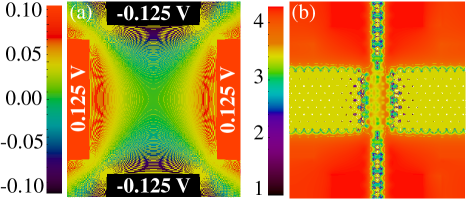
In order to create such an initial potential profile, we iteratively solve the two-dimensional (2D) Laplace equation
| (19) |
for a hypothetical system where the central region is empty while using the following boundary conditions: (i) the initial potential in the central region is zero or may be the same as the potentials of the four leads, (ii) the potential in every lead is unchanged; and (iii) the potential toward the vacuum region, that is, at the corners of the box, decays. We use the same solution for each 2D -plane lined up along the -axis to compose the three-dimensional (3D) real-space grid which encloses the central device region.
This auxiliary solution provides an initial guess for the electrostatic potential profile with boundary conditions set by the voltages of the leads, which is illustrated in Fig. 5(a) for mGNR-sCNT crossbar from Fig. 1(a) with empty central region. The Poisson equation for the same mGNR-sCNT crossbar is then updated via the self-consistent loop until the converged solution shown in Fig. 5(b) is reached. In practice, we find that using solution like the one in Fig. 5(a) as the first iteration significantly accelerates the convergence. Once the potential and the charge density are converged, the final result is independent of the initial guess.
4 Zero-bias transmission coefficients of GNR-CNT crossbars
In this section, we consider quantum transport quantities that are relevant for the description of the linear-response regime in crossbars depicted in Fig. 1. In that case, DFT Hamiltonian computed in equilibrium yields the transmission coefficients in Eq. (7) where all . The integration of the transmission coefficients yields the conductance coefficients at finite temperature
| (20) |
where and in the absence of external magnetic field Datta1995 ; Buttiker1986 . The conductance coefficients connect current in electrode to voltages applied to electrodes via the multiterminal Landauer-Büttiker formula Ferry2009 ; Datta1995 ; Buttiker1986
| (21) |
which is the linear-response limit simplification of Eq. (6).
The zero-bias transmission coefficients along GNR, CNT and between GNR and CNT for three devices in Figs. 1 are shown in Fig. 3. In addition, dashed line in subpanels (a) in each of these three Figs. shows quantized zero-bias transmission function of an isolated infinite homogeneous GNR attached to two macroscopic reservoirs, while dashed line in subpanels (b) shows the same information for an isolated infinite homogeneous CNT. This allows one to visually estimate the impact of the proximity of GNR on the linear-response transport properties of CNT and vice versa. In all cases plotted in Fig. 3 we find sizable transmission coefficient which signifies non-tunneling nature of transport between crossed GNR and CNT in junctions shown in Fig. 1.
5 Current-voltage characteristics of GNR-CNT crossbars
In this section we consider nonequilibrium quantum transport in CNT electrode 3 of devices depicted in Fig. 1, which is driven by finite bias voltage and, therefore, far outside the linear-response regime discussed in Sec. 4. The bias voltage is applied between electrodes 1 and 3, as well as 2 and 3, labeled in Fig. 1(d). This means that current plotted in Fig. 4 has contribution from two electron fluxes, and , which are summed via Eq. (6). We use convention that current is positive in electrode if it flows into this electrode (i.e., electrons are flowing out of electrode 3 in Fig. 4 for positive bias voltage ). We use K in Eq. (8) while neglecting any inelastic scattering processes that would add additional self-energies into Eq. (4), thereby making usage of NEGF-DFT beyond atomic orbitals prohibitively computationally expensive Frederiksen2007 .
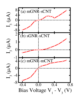
Unlike experiments on CNT-CNT crossbars Fuhrer2000 , where intertube current (i.e., equivalent of our current ) was measured A at forward bias voltage V in mCNT-sCNT device (at K), the current in all three of our crossbars is an order of magnitude larger at similar bias voltage. This is due to the overlap of orbitals on C atoms of GNR and CNT (see Fig. 6) which introduces non-negligible effective hopping between them, so that transport is not governed solely by quantum tunneling through the vacuum gap as in CNT-CNT crossbars.
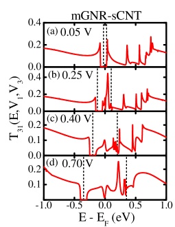
The most interesting feature of vs. curves in Fig. 4 is NDR shown in Fig. 4(a) for mGNR-sCNT crossbar. The applications of devices exhibiting NDR in microwave, switching, and memory devices requires low onset voltage and a high peak-to-valley current ratio (PVCR) to reduce power consumption and improve the efficiency. For example, a key requirement of NDR devices for use in embedded memory applications is a low valley current to reduce the standby power consumption while concurrently having a sufficient peak current to charge the parasitic node capacitance. The NDR exhibited by mGNR-sCNT crossbar in Fig. 4(a) has parameters V and .
We can compare this with three-terminal (based on FET configuration) large-area graphene NDR device recently fabricated by the IBM team Wu2012 which exhibited V and . The onset of NDR behavior can be shifted by the gate voltage in this device, but it remains above 1 V. NDR was also observed Bushmaker2009 in suspended quasi-metallic single-walled CNTs where applying a gate voltage switches I–V characteristics from Ohmic behavior to nonlinear behavior with V and . Previously explored semiconductor devices with low V and high include trench-type InGaAs/InAlAs quantum-wire-FET at 40 K in a simple three-terminal configuration in which NDR can also be controlled by the gate voltage Jang2003 .
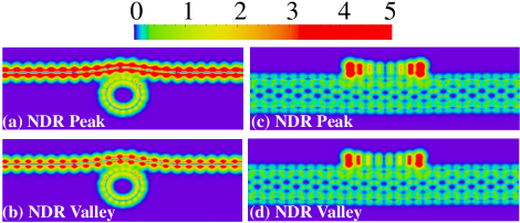
The origin of NDR in this system of noninteracting quasiparticles is explained in Fig. 5 which plots the transmission coefficient as a function of the bias voltage. At the onset of NDR, transmission peak enters the bias voltage window in Fig. 5(b), while at the NDR valley transmission coefficient within the larger bias window is reduced in Fig. 5(c). Additional information is provided by the local density of states (LDOS) at finite bias voltage which is plotted in Fig. 6. The LDOS becomes enhanced at NDR peak both along the edges of ZGNR and in its interior.
6 Concluding remarks
In conclusion, using the NEGF-DFT framework for first-principles quantum transport modeling, which was originally developed for two-terminal devices and recently extended to multiterminal ones, we have analyzed current between GNR and single-walled CNT where electrons traverse the vacuum gap between them. The GNR covers CNT over a nanoscale region where their overlap contains only carbon and hydrogen atoms. Following up on the recent experimental fabrication of GNR-CNT crossbars Jiao2010 , as well as previous experiments on CNT-CNT crossbars Fuhrer2000 , we have investigated three examples of GNR-CNT crossbars combining metallic and semiconducting crossed nanowires.
While all three types of four-terminal GNR-CNT crossbars exhibit nonlinear current-voltage I–V characteristics, which is asymmetric with respect to changing the bias voltage from positive to negative, mGNR-sCNT crossbar also exhibits NDR with low onset voltage V and peak-to-valley current ratio . The origin of NDR is examined by looking at the transmission coefficient between GNR and CNT semi-infinite electrodes and local density of states at finite bias voltage.
We also provide an overview of essential computational issues that have to be tackled when extending NEGF-DFT framework to nanojunctions containing more that two electrodes Saha2009 ; Saha2010a ; Saha2010 ; Saha2011 .
Acknowledgements.
We thank V. Meunier for illuminating discussions. Financial support from NSF under Grant No. ECCS 1202069 is gratefully acknowledged. The supercomputing time was provided in part by NSF through XSEDE resource TACC Stampede.References
- (1) A. K. Geim, Graphene: Status and prospects, Science 324, 1530 (2009)
- (2) S. Das Sarma, S. Adam, E. H. Hwang, and E. Rossi, Electronic transport in two-dimensional graphene, Rev. Mod. Phys. 83, 407 (2011)
- (3) A. R. Botello-Méndez, E. Cruz-Silva, J. M. Romo-Herrera, F. López-Urias, M. Terrones, B. G. Sumpter, H. Terrones, J.-C. Charlier, and V. Meunier, Quantum transport in graphene nanonetworks, Nano Lett. 11, 3058 (2011)
- (4) K. M. M. Habib and R. K. Lake, Current modulation by voltage control of the quantum phase in crossed graphene nanoribbons, Phys. Rev. B 86, 045418 (2012)
- (5) F. Schwierz, Graphene transistors, Nature Nanotechn. 5, 487 (2010)
- (6) A. F. Young and P. Kim, Electronic transport in graphene heterostructures, Annu. Rev. Condens. Matter Phys. 2, 101 (2011)
- (7) V. H. Nguyen, J. Saint-Martin, D. Querlioz, F. Mazzamuto, A. Bournel, Y.-M. Niquet, and P. Dollfus, Bandgap nanoengineering of graphene tunnel diodes and tunnel transistors to control the negative differential resistance, J. Comp. Electron. 12, 85 (2013)
- (8) D. Pesin and A. H. MacDonald, Spintronics and pseudospintronics in graphene and topological insulators, Nature Mater. 11, 409 (2012)
- (9) R. W. Keyes, Physical limits of silicon transistors and circuits, Rep. Prog. Phys. 68, 2701 (2005)
- (10) S. Agnoli and G. Granozzi, Second generation graphene: Opportunities and challenges for surface science, Surface Science 609, 1 (2013)
- (11) L. Jiao, L. Zhang, L. Ding, J. Liu, , and H. Dai, Aligned graphene nanoribbons and crossbars from unzipped carbon nanotubes, Nano Res. 3, 387 (2010)
- (12) W. Lu, P. Xie, and C. M. Lieber, Nanowire transistor performance limits and applications, IEEE Trans. Elec. Dev. 55, 2859 (2008)
- (13) M. S. Fuhrer, J. Nygård, L. Shih, M. Forero, Y.-G. Yoon, M. S. C. Mazzoni, H. J. Choi, J. Ihm, S. G. Louie, A. Zettl, and P. L. McEuen, Crossed nanotube junctions, Science 288, 494 (2000)
- (14) G. Stefanucci and R. van Leeuwen, Nonequilibrium Many-Body Theory of Quantum Systems: A Modern Introduction (Cambridge University Press, Cambridge, 2013)
- (15) T. Christen and M. Büttiker, Gauge-invariant nonlinear electric transport in mesoscopic conductors, Europhys. Lett. 35, 523 (1996)
- (16) S. Sanvito, Chapter 7 in Computational Nanoscience, ed. by E. Bichoutskaia (RSC Publishing, Cambridge, 2011)
- (17) D. A. Areshkin and B. K. Nikolić, Electron density and transport in top-gated graphene nanoribbon devices: First-principles Green function algorithms for systems containing a large number of atoms, Phys. Rev. B 81, 155450 (2010).
- (18) J. Taylor, H. Guo, and J. Wang, Ab initio modeling of quantum transport properties of molecular electronic devices, Phys. Rev. B 63, 245407 (2001)
- (19) M. Brandbyge, J.-L. Mozos, P. Ordejón, J. Taylor, and K. Stokbro, Density-functional method for nonequilibrium electron transport, Phys. Rev. B 65, 165401 (2002)
- (20) J. J. Palacios, A. J. Pérez-Jiménez, E. Louis, E. Sanfabián, and J. A. Vergés, First-principles approach to electrical transport in atomic-scale nanostructures, Phys. Rev. B 66, 035322 (2002)
- (21) A. R. Rocha, V. M. García-Suárez, S. Bailey, C. Lambert, J. Ferrer, and S. Sanvito, Spin and molecular electronics in atomically generated orbital landscapes, Phys. Rev. B 73, 085414 (2006)
- (22) K. Stokbro, First-principles modeling of electron transport, J. Phys.: Condens. Matter 20, 064216 (2008)
- (23) http://www.quantumwise.com
- (24) http://nanoacademic.ca/index.jsp
- (25) http://www.icmab.es/siesta/
- (26) http://www.smeagol.tcd.ie
- (27) http://www.dfa.ua.es/en/invest/condens/Alacant/
- (28) https://wiki.fysik.dtu.dk/gpaw/
- (29) J. Chen, K. S. Thygesen, and K. W. Jacobsen, Ab initio nonequilibrium quantum transport and forces with the real-space projector augmented wave method, Phys. Rev. B 85, 155140 (2012)
- (30) K. K. Saha, W. Lu, J. Bernholc, and V. Meunier, First-principles methodology for quantum transport in multiterminal junctions, J. Chem. Phys. 131, 164105 (2009)
- (31) K. K. Saha, W. Lu, J. Bernholc, and V. Meunier, Electron transport in multiterminal molecular devices: A density functional theory study, Phys. Rev. B 81, 125420 (2010)
- (32) K. K. Saha, B. K. Nikolić, V. Meunier, W. Lu, and J. Bernholc, Quantum-interference-controlled three-terminal molecular transistors based on a single ring-shaped molecule connected to graphene nanoribbon electrodes, Phys. Rev. Lett. 105, 236803 (2010)
- (33) K. K. Saha, T. Markussen, K. S. Thygesen, and B. K. Nikolić, Multiterminal single-molecule–graphene-nanoribbon junctions with the thermoelectric figure of merit optimized via evanescent mode transport and gate voltage, Phys. Rev. B 84, 041412(R) (2011)
- (34) D. K. Ferry, S. M. Goodnick, and J. P. Bird, Transport in Nanostructures (Cambridge University Press, Cambridge, 2009)
- (35) H. Ren, Q.-X. Li, Y. Luo, and J. Yang, Graphene nanoribbon as a negative differential resistance device, Appl. Phys. Lett. 94, 173110 (2009)
- (36) Y. Wu, D. B. Farmer, W. Zhu, S.-J. Han, C. D. Dimitrakopoulos, A. A. Bol, P. Avouris, and Y.-M. Lin, Three-terminal graphene negative differential resistance devices, ACS Nano 6, 2610 (2012)
- (37) Y.-W. Son, M. L. Cohen, and S. G. Louie, Energy gaps in graphene nanoribbons, Phys. Rev. Lett. 97, 216803 (2006)
- (38) Y. Matsuda, J. Tahir-Kheli, and W. A. Goddard, Definitive band gaps for single-wall carbon nanotubes, J. Phys. Chem. Lett. 1, 2946 (2010)
- (39) M. Ouyang, J.-H. Huang, C. L. Cheung, and C. M. Lieber, Energy gaps in “metallic” single-walled carbon nanotubes, Science 292, 702 (2001)
- (40) O. V. Yazyev and M. I. Katsnelson, Magnetic correlations at graphene edges: Basis for novel spintronics devices, Physical Review Letters 100, 047209 (2008)
- (41) J. Kunstmann, C. Özdoğan, A. Quandt, and H. Fehske, Stability of edge states and edge magnetism in graphene nanoribbons, Phys. Rev. B 83, 045414 (2011)
- (42) D. A. Areshkin and C. T. White, Building blocks for integrated graphene circuits, Nano Lett. 7, 3253 (2007)
- (43) X. Jia, M. Hofmann, V. Meunier, B. G. Sumpter, J. Campos-Delgado, J. Manuel, R.-H. Hyungbin, S. Ya-Ping, H. A. Reina, J. Kong, M. Terrones, and M. S. Dresselhaus, Controlled formation of sharp zigzag and armchair edges in graphitic nanoribbons, Science 323, 1701 (2009)
- (44) P.-H. Chang and B. K. Nikolić, Edge currents and nanopore arrays in zigzag and chiral graphene nanoribbons as a route toward high- thermoelectrics, Phys. Rev. B 86, 041406 (2012)
- (45) G. Kresse and J. Hafner, Ab initio molecular dynamics for liquid metals, Phys. Rev. B 47, 558 (1993)
- (46) G. Kresse and J. Furthmüller, Efficient iterative schemes for ab initio total-energy calculations using a plane-wave basis set, Phys. Rev. B 54, 11169 (1996)
- (47) G. Kresse and J. Furthmüllerb, Efficiency of ab-initio total energy calculations for metals and semiconductors using a plane-wave basis set, Comput. Mater. Sci. 6, 15 (1996)
- (48) P. E. Blöchl, Projector augmented-wave method, Phys. Rev. B 50, 17953 (1994)
- (49) G. Kresse and D. Joubert, From ultrasoft pseudopotentials to the projector augmented-wave method, Phys. Rev. B 59, 1758 (1999)
- (50) J. P. Perdew, K. Burke, and M. Ernzerhof, Generalized gradient approximation made simple, Phys. Rev. Lett. 77, 3865 (1996)
- (51) H.-P. Breuer and F. Petruccione, The Theory of Open Quantum Systems (Oxford University Press, Oxford, 2002)
- (52) C. Timm, Tunneling through molecules and quantum dots: Master-equation approaches, Phys. Rev. B 77, 195416 (2008)
- (53) S. Koller, M. Grifoni, M. Leijnse, and M. R. Wegewijs, Density-operator approaches to transport through interacting quantum dots: Simplifications in fourth-order perturbation theory, Phys. Rev. B 82, 235307 (2010)
- (54) S. Datta, Electronic transport in mesoscopic systems (Cambridge University Press, Cambridge, 1995)
- (55) S. Barraza-Lopez, Coherent electron transport through freestanding graphene junctions with metal contacts: a materials approach, J. Comp. Electron. 12, 145 (2013)
- (56) T. B. Boykin, M. Luisier, G. Klimeck, X. Jiang, N. Kharche, Y. Zhou, and S. K. Nayak, J. Appl. Phys. 109, 104304 (2011)
- (57) C. Fiolhais, F. Nogueira, and M. A. L. Marques, Eds., A Primer in Density Functional Theory (Lecture Notes in Physics Vol. 620) (Springer-Verlag, Berlin, 2003)
- (58) I. Rungger and S. Sanvito, Algorithm for the construction of self-energies for electronic transport calculations based on singularity elimination and singular value decomposition, Phys. Rev. B 78, 035407 (2008)
- (59) F. Mahfouzi and B. K. Nikolić, How to construct the proper gauge-invariant density matrix in steady-state nonequilibrium: Applications to spin-transfer and spin-orbit torques, arXiv:1305.3180 (2013)
- (60) M. Büttiker, Four-terminal phase-coherent conductance, Phys. Rev. Lett. 57, 1761 (1986)
- (61) T. Frederiksen, M. Paulsson, M. Brandbyge, and A.-P. Jauho, Inelastic transport theory from first principles: Methodology and application to nanoscale devices, Phys. Rev. B 75, 205413 (2007)
- (62) A. W. Bushmaker, V. V. Deshpande, S. Hsieh, M. W. Bockrath, and S. B. Cronin, Gate voltage controllable non-equilibrium and non-ohmic behavior in suspended carbon nanotubes, Nano Lett. 9, 2862 (2009)
- (63) K.-Y. Jang, T. Sugaya, C.-K. Hahn, M. Ogura, K. Komori, A. Shinoda, and K. Yonei, Negative differential resistance effects of trench-type InGaAs quantum-wire field-effect transistors with 50-nm gate-length, Appl. Phys. Lett. 83, (2003)