Wigner and Kondo physics in quantum point contacts
revealed by scanning gate microscopy
Abstract
Quantum point contacts exhibit mysterious conductance anomalies in addition to well known conductance plateaus at multiples of . These 0.7 and zero-bias anomalies have been intensively studied, but their microscopic origin in terms of many-body effects is still highly debated. Here we use the charged tip of a scanning gate microscope to tune in situ the electrostatic potential of the point contact. While sweeping the tip distance, we observe repetitive splittings of the zero-bias anomaly, correlated with simultaneous appearances of the 0.7 anomaly. We interpret this behaviour in terms of alternating equilibrium and non-equilibrium Kondo screenings of different spin states localized in the channel. These alternating Kondo effects point towards the presence of a Wigner crystal containing several charges with different parities. Indeed, simulations show that the electron density in the channel is low enough to reach one-dimensional Wigner crystallization over a size controlled by the tip position.
I Introduction
Quantum point contacts van-Wees-1988 (QPCs) are among the simplest quantum devices made out of a two-dimensional electron gas (2DEG). Applying a negative voltage on a split-gate creates a quasi-one-dimensional (1D) channel connected to large 2D reservoirs. This narrow channel behaves as an electron wave-guide and transmits a finite number of modes, each of them carrying one quantum of conductance ( is the electron charge and the Planck constant). As a result, the conductance versus gate voltage curve shows a series of quantized plateaus with transitions which are well reproduced by a single-particle model Buttiker-1990 .
However, since the early days of QPCs, a shoulder-like feature is commonly observed Thomas-1996 at a conductance around 0.7 , which cannot be explained by single-particle theories. With lowering temperature, this “0.7 anomaly” rises to reach the first plateau, and a zero-bias peak called “zero-bias anomaly” (ZBA) emerges in the non-linear differential conductance Cronenwett-2002 . These anomalies have been extensively studied through transport experiments Thomas-1996 ; Kristensen-2000 ; Cronenwett-2002 ; Reilly-2002 ; Hew-2008 , revealing the complexity of the underlying phenomena. Different theoretical models have been proposed Wang-1998 ; Spivak-2000 ; Sushkov-2001 ; Meir-2002 ; Matveev-2004 ; Rejec-2006 , but no consensus could be reached so far on their interpretation Micolich-2011 .
Recently, an experiment using several gates to vary the channel length Iqbal-2013a revealed the possible existence of several emergent localized states responsible for the conductance anomalies. At the same time, a different theoretical model was proposed Bauer-2013 , explaining the anomalies without invoking localized states in the channel. As stressed in Ref. Micolich-2013 , investigating these anomalies using scanning probe techniques could make it possible to check the existence of spontaneously localized states and discriminate between these two proposals: this is the aim of the present letter.
Here we perform scanning gate microscopy Eriksson-1996 (SGM), in which a negatively charged tip is scanned above the sample surface and modifies the electrostatic potential in the 2DEG. This local potential change induces electron back-scattering towards the QPC, which can be used to image single-particle phenomena such as wave-function quantization in the channel Topinka-2000 , branched flow in the disorder potential Topinka-2001 , interference patterns induced by the tip Leroy-2005 ; Jura-2007 ; Kozikov-2013 , or to investigate electron-electron interactions inside Freyn-2008 or outside Jura-2010 the QPC. This movable gate can also be used to tune in situ the saddle potential of the QPC, in a more flexible and less invasive way than fixed surface gates, and probe intrinsic properties of the QPC such as the 0.7 anomaly Crook-2006 ; Iagallo-2013 .
Here we show that approaching the tip towards the QPC produces an oscillatory splitting of the ZBA, correlated with simultaneous appearances of the 0.7 anomaly, thereby confirming that both features share a common origin Cronenwett-2002 ; Iqbal-2013a . We interpret these observations as the signature of a small one-dimensional Wigner crystal Wigner-1934 ; Schulz-1993 ; Deshpande-2008 forming in the channel Hew-2009 (a quantum chain of charges localized by Coulomb interactions in absence of disorder). The number of charges in this many-body correlated state is tuned by changing the tip position, leading alternatively to a single- or a two-impurity Kondo effect (screening of a localized spin by conducting electrons), with a conductance peak either at zero, or at finite bias, depending on the charge parity.
Our observations therefore strongly support the existence of emergent localized states, as suggested in Ref. Iqbal-2013a where the number of localized charges is controlled by changing the effective channel length. Here we show that a similar effect is observed when changing the distance of an additional gate placed around the QPC. To understand this new result, we perform classical electrostatic simulations and evaluate the size of the region where electrons should form a 1D Wigner crystal thanks to the critically low electron density. We show that the calculated size of this small crystal is in good agreement with the observed change in the number of localized charges, thereby revealing that Wigner crystallization is, to our opinion, the correct way to understand this spontaneous localization.
II Results
Transport measurements
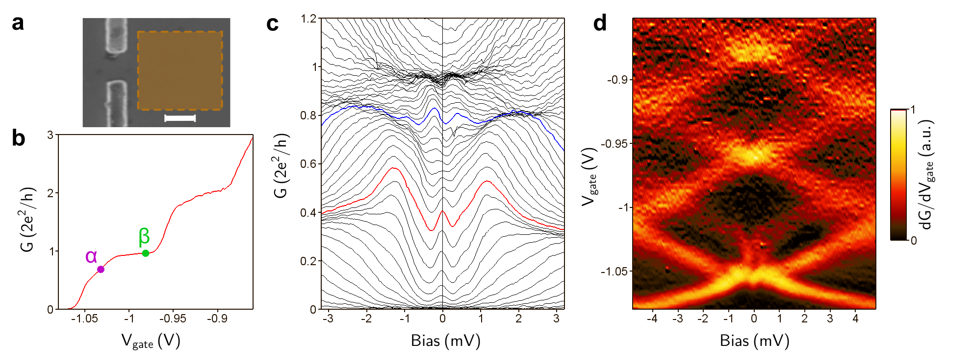
The QPC (see Methods and Fig. 1a) is cooled down to a temperature of 20 mK in a cryogenic scanning probe microscope Hackens-2010 . In the absence of the tip (moved several microns away), the linear conductance shows the usual staircase behaviour versus gate voltage (Fig. 1b). The shoulder below the first quantized plateau is the puzzling 0.7 anomaly. The source-drain bias spectroscopy (Fig. 1c) shows that this shoulder evolves to a clear plateau at 0.85 at finite bias Patel-1991 ; Thomas-1998 ; Kristensen-2000 . The narrow peak around zero bias is the ZBA and disappears above 1 K (Supplementary Figure 1). Its width of 200 eV is much smaller than the 1D subband spacing of 4.5 meV (Fig. 1d). Above 0.7 , the ZBA splits into finite-bias peaks Iqbal-2013a ; Komijani-2013 centred at 250 V. We show in the following that the presence of the 0.7 anomaly is related to this splitting of the ZBA.
Scanning gate microscopy
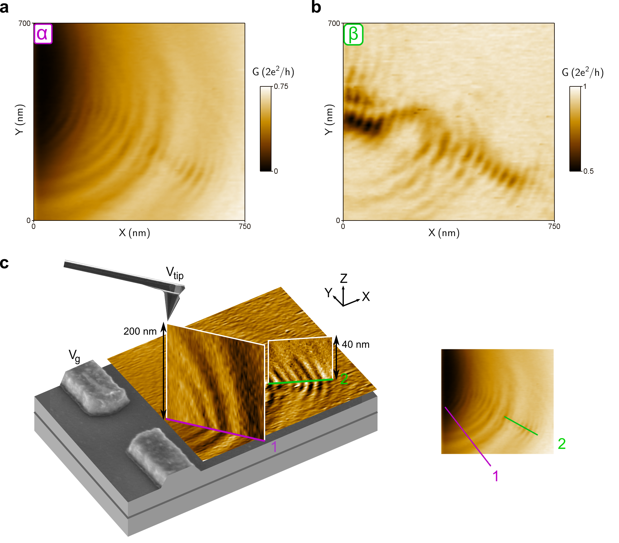
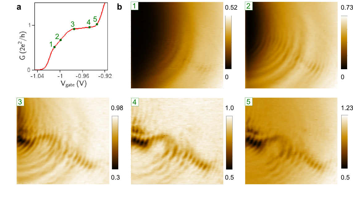
When the tip is scanned near the QPC and polarized such as to deplete locally the 2DEG (see Methods), we observe two distinct phenomena. On the first conductance plateau (Fig. 2b), SGM images reveal the electron flow coming out of the QPC, with fringes spaced by half the Fermi wavelength, as already observed by several groups Topinka-2001 ; Jura-2007 ; Kozikov-2013 . The fringes result from interferences of electrons backscattered by the depleted region below the tip and reflected by impurities Topinka-2001 ; Jura-2007 in the 2DEG or directly by the gates Leroy-2005 ; Jura-2009 .
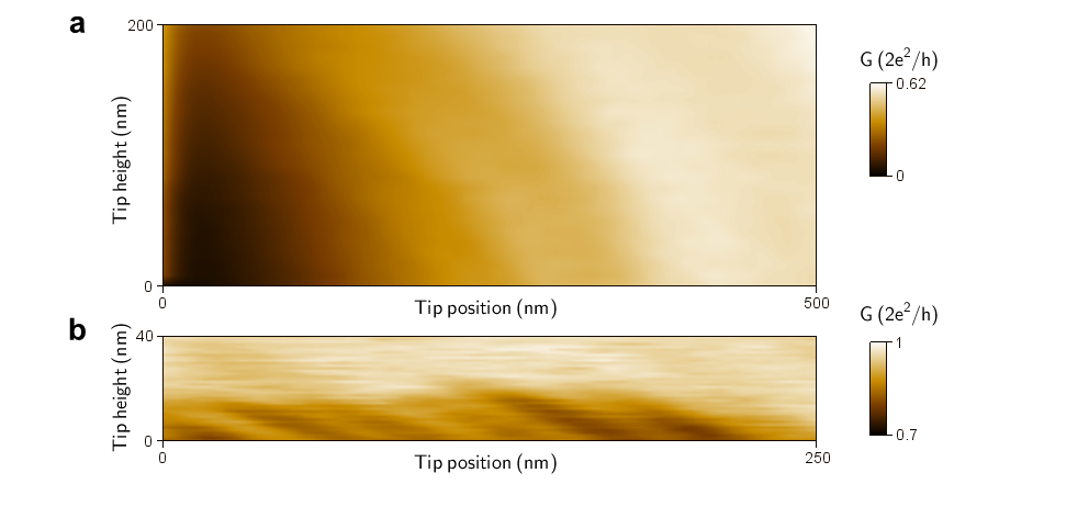
Below the first plateau (Fig. 2a), SGM maps reveal a novel set of concentric rings centred on the QPC, with a spacing increasing with tip distance (see also Supplementary Figure 2). As opposed to the previous one-particle interference fringes, these new rings are not linked to the electron flow (black region in Fig. 2b) but extend rather isotropically around the QPC, not only in the horizontal plane but in all three directions of space. This is revealed by scanning the tip in a vertical plane (Fig. 2c), unveiling half spheres centred on the QPC (purple line 1). This behaviour contrasts with that of interference fringes (green line 2) that quickly disappear when the tip is scanned more than 50 nm above the surface (see also Supplementary Figure 3). Interferences indeed require electrons at the Fermi level to be backscattered by a depleted region below the tip, a situation which is only obtained for the tip close enough to the 2DEG (and at low enough temperature to avoid thermal averaging of the interferences). We therefore conclude that the new rings are not interferences but result from a direct tuning of the electrostatic potential in the QPC. The larger ring spacing at larger distances results from the smaller potential changes induced by the tip.
Conductance anomalies
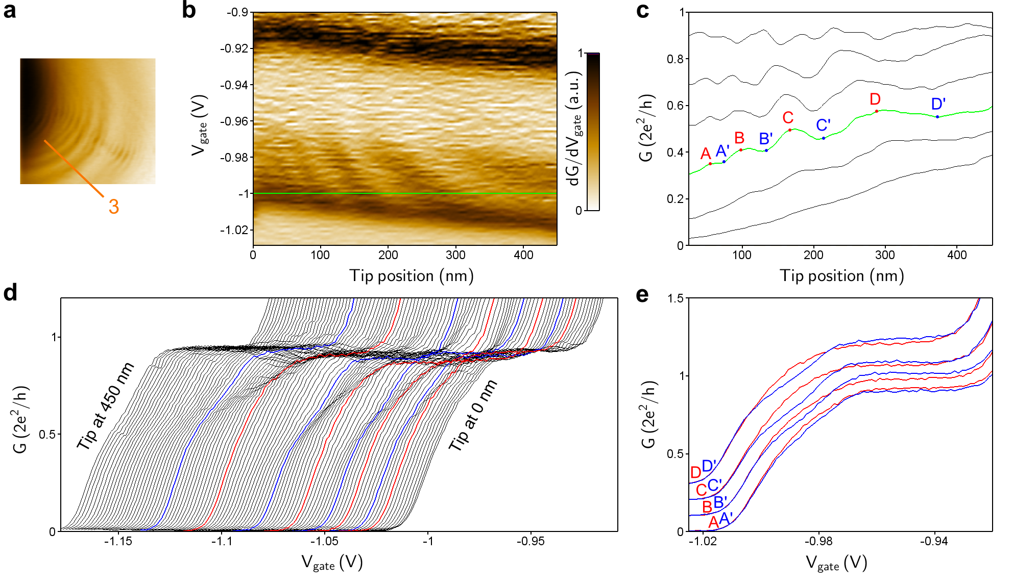
To demonstrate that these rings correspond to modulations of the conductance anomalies, the tip is scanned along a single line in a region with almost no interference (line 3 in Fig. 3a) and the QPC parameters (gate and bias voltages) are varied. Fig. 3b shows that the ring-related conductance oscillations are only visible for gate voltages in the transition below the first plateau, just where the ZBA and 0.7 anomaly are observed. Fig. 3c shows how the conductance oscillations evolve when the average conductance goes from 0 to while changing the gate voltage. The oscillations are clearly visible between 0.4 and 0.8 . They are blurred when approaching because some interference fringes come into play. The increasing distance between conductance extrema (labeled A to D for maxima and A’ to D’ for minima) is consistent with an oscillatory phenomenon in the QPC, controlled by the decreasing electrostatic coupling to the tip. Plotting the conductance versus gate voltage (Fig. 3d) reveals the oscillatory behaviour of the 0.7 anomaly. The amplitude of this modulation can be read from Fig. 3e, where curves at positions X and X’ are compared two-by-two (curves are shifted horizontally to compensate for the drift of the pinch-off voltage while approaching the tip). Curves at positions A to D are smooth with no shoulder, i.e. no anomaly, whereas curves at positions A’ to D’ present a reduced conductance above 0.5 , i.e. the 0.7 anomaly. The concentric rings observed in SGM images (Fig. 2a) therefore correspond to an alternating modulation of the 0.7 anomaly when the tip approaches the QPC.
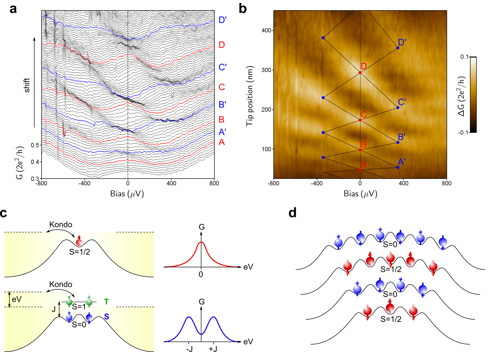
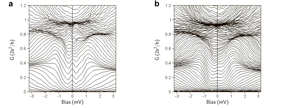
We now analyse the behaviour of the ZBA when the 0.7 anomaly repeatedly appears and disappears, and show that both anomalies are linked. Fig. 4a shows the differential conductance versus source-drain bias for different tip positions (same scan line as in Fig. 3a). Curves at positions A to D have a peak centred at zero bias (ZBA), whereas curves at positions A’ to D’ have a dip at zero bias and local maxima at 250 V bias (splitting of the ZBA), on top of the same V-shaped background. Scanning the SGM tip therefore produces a repetitive splitting of the ZBA, that draws a checkerboard pattern in a color-plot of the spectroscopy versus tip position (Fig. 4b). Note that the spontaneous splitting of the ZBA observed without the tip (Fig. 1c) also shows peaks at 250 V and probably has the same origin.
Considering the regularity of the concentric rings in Fig. 2a, this oscillatory behaviour of the 0.7 and zero-bias anomalies would be observed for any scanning line in a large range of angles (see Supplementary Figure 4 and Supplementary Note 1). As a consequence, rings with conductance maxima correspond to a simple staircase in the linear conductance and a ZBA in the non-linear spectroscopy, whereas rings with conductance minima correspond to a 0.7 anomaly and a splitting of the ZBA. This result shows that the ZBA suppresses the 0.7 anomaly at low temperature Cronenwett-2002 only if the ZBA is not split into finite-bias peaks.
III Discussion
First, we would like to stress again that these new conductance oscillations cannot be explained by interference effects in the 2DEG. One argument already given above is that interferences require backscattering with a tip close to the surface, whereas the new rings are observed up to large tip heights (Fig. 2c). A second argument is that interference fringes would have an increasing spacing for short tip distances because the density is reduced close to the QPC and the electron wavelength is larger, but the opposite behaviour is observed.
We now discuss a possible single-particle effect inside the QPC that, at first sight, could give similar conductance oscillations. In case of a non-adiabatic transmission, wave-functions are scattered by the QPC potential barrier and transmission resonances appear when the barrier length is equal to an integer number of half the longitudinal wavelength. If the effect of the tip is to change the channel length, such resonances could give conductance oscillations versus tip distance. However, this single-particle mechanism cannot explain the repetitive splittings of the ZBA which are simultaneous with the observed conductance oscillations and we therefore need another explanation.
The ZBA in QPCs has been shown to scale with temperature and magnetic field like the Kondo effect in quantum dots Cronenwett-2002 . This effect corresponds to the screening of a single degenerate level by a continuum of states, and therefore indicates the presence of a localized spin in the QPC channel Meir-2002 . Splittings of the ZBA have been observed recently in length-tunable QPCs Iqbal-2013a and interpreted as a two-impurity Kondo effect Georges-1999 ; Aguado-2000 , involving non-equilibrium Kondo screening Lopez-2002 ; Kiselev-2003 , as commonly observed in quantum dots with even numbers of electrons Sasaki-2000 , coupled quantum dots Jeong-2001 , and molecular junctions Roch-2008 .
We now consider different scenarios to explain the presence of such localized states in our system. In a recent work on QPCs made out of a two dimensional hole gas, a spontaneous splitting of the ZBA as the QPC opens has been reported Komijani-2013 . This effect was attributed to a charge impurity forming a potential well close to the channel, containing one or two charges, leading to different types of Kondo screening. In our case, the spontaneous splitting of the ZBA as the QPC opens (Fig. 1c) could be explained by this effect. However, the fact that approaching the tip towards the QPC results in 4 successive splittings of the ZBA indicates that this impurity should contain at least 8 charges, which is unlikely for a single impurity. Nevertheless, one could imagine that a shallow quantum dot has formed in the QPC due to potential fluctuations induced by residual disorder Nixon-1991 and giving Coulomb blockade oscillations as often observed in long 1D wires Staring-1992 . The major argument to exclude this scenario is that the split-gate has a larger capacitive coupling to the channel than the tip has (i.e. a larger lever-arm parameter), so the split-gate should induce more charging events than the tip, but we observe the opposite: approaching the tip by 600 nm produces four successive splittings of the ZBA and sweeping the gate voltage produces only one splitting. It can therefore not be Coulomb blockade in a disorder-induced quantum dot.
The only remaining possibility to explain the presence of localized states in the channel is a spontaneous electron localization which is not induced by potential barriers but instead by electron-electron interactions. Indeed, a large number of theoretical and numerical investigations show that interactions can localize a finite number of electrons in the channel Sushkov-2003 ; Matveev-2004 ; Rejec-2006 ; Guclu-2009 . On the first conductance plateau and below, transport can be considered as 1D, and the electron density is so low that the Coulomb repulsion overcomes the kinetic energy. When the 1D density fulfills the criterion , where is the effective Bohr radius (10 nm in GaAs), electrons are expected to spontaneously order in a crystal, with an inter-particle distance minimizing Coulomb repulsion Shulenburger-2008 . This many-body state, known as a Wigner crystal Wigner-1934 ; Schulz-1993 , has been suggested to be responsible for the 0.7 anomaly in QPCs Matveev-2004 . When the electron density in the channel is decreased below the critical value, the density modulations evolve continuously from the periodicity of Friedel oscillations to the periodicity of the Wigner crystal Soffing-2009 . Quantum Monte Carlo simulations have also shown that electrons in the crystallized region can be relatively decoupled from the high density reservoirs and present an antiferromagnetic coupling between adjacent spins Guclu-2009 . In contrast to the case of quantum dots with real tunnel barriers, electron localization in a QPC is not straightforward, and results from emergent barriers in the self-consistent potential. On the other hand, the Kondo effect requires a relatively open system with a good coupling to the reservoirs, and this makes the QPC a suitable platform to observe Kondo phenomena on an interaction-induced localized state, as shown recently in length-tunable QPCs Iqbal-2013a .
This last scenario being the most realistic one in our case, we therefore interpret the four observed oscillations as a signature of eight successive states of a small non-uniform 1D Wigner crystal with an alternating odd and even number of localized charges. Situations with an odd number of electrons in a spin ground state show a ZBA due to Kondo screening of non-zero spin states. Situations with an even number of electrons in a spin singlet ground state show a splitting of the ZBA due to non-equilibrium Kondo screening Lopez-2002 ; Kiselev-2003 of the spin triplet excited state with peaks at a finite bias (Fig. 4c). The four oscillations, suggestive of eight successive states, reveal that a large number of electrons can spontaneously localize in the channel of a QPC, as shown in Fig. 4d. Observing Kondo screening on a system with many localized charges is not so surprising if we compare to quantum dots where the Kondo effect is observed up to large numbers of electrons Goldhaber-Gordon-1998 . Nevertheless, the particular case of a 1D chain of localized charges in the Kondo regime still requires theoretical investigations.
This analysis is consistent with the interpretation given in Ref. Iqbal-2013a for similar observations using a QPC with six surface gates to tune the channel length. Our SGM experiment brings additional information on this effect, since scanning the tip around the QPC, laterally or vertically, changes the shape, extension, and symmetry of the channel potential. The circular and almost isotropic rings in Fig. 2c show that the localized states survive to all these potential deformations. The regularity of the successive rings also suggests that this localization occurs rather independently of disorder, though possible crystal pinning effects should be investigated in the future.
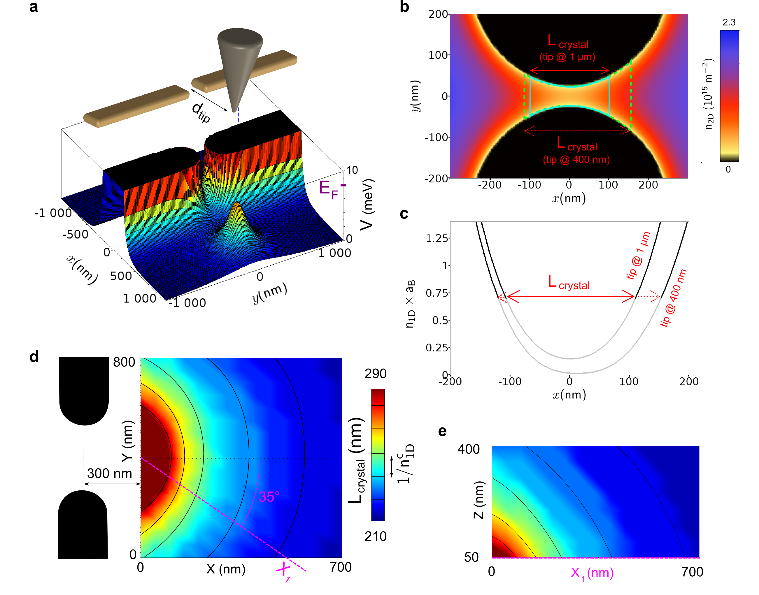
In Ref. Iqbal-2013a , the parameter controlling the number of localized states is the effective length of the channel, defined in Ref. Iqbal-2013 and computed using an analytical approach assuming a fixed zero potential at the surface Davies-1995 . This method is not suitable to model our SGM experiment, as the tip is situated above the surface. To evaluate the potential landscape in presence of the tip, we perform 3D classical electrostatic simulations in the Thomas-Fermi approximation (see Methods and Supplementary Note 2) and compute self-consistently the local potential in the 2DEG and the local 2D electronic density (Fig. 5a). In this way, the tip-induced potential is correctly calculated, with the screening effects from the 2DEG and the metallic gates taken into account. We obtain a good agreement between calculated and experimental values regarding the gate voltage required to close the QPC, the tip voltage to reach depletion in the 2DEG, and the cross-talk between the tip position and the QPC opening. The effective channel length used in Ref. Iqbal-2013a was calculated in Ref. Iqbal-2013 , using the unscreened gate potential. This length cannot be calculated here from our self-consistent potential, because screening effects induce non-parabolic transverse confinement potentials.
We propose instead that the parameter controlling the number of localized charges is the size of the region where the 1D Wigner crystallization should occur. This interaction-induced spontaneous ordering is often discussed in terms of the Wigner-Seitz radius , representing the ratio of the Coulomb repulsion to the kinetic energy. A recent numerical investigation of the 1D Wigner crystallization shows that the critical parameter varies between 0.5 and 2, depending on the strength of the transverse confinement potential Shulenburger-2008 . To evaluate the size of the region where is larger than a given threshold, we calculate the 1D electron density by integration of the 2D electron density in the transverse direction (Fig. 5b and 5c). As an example, we choose a critical value corresponding to a critical density , and evaluate the size where the density is lower than . This size is found to vary from 210 to 290 nm when the tip is approached by 600 nm towards the QPC, which shows that the tip can strongly affect the size of the low density region, and hence the number of localized charges. The tip positions leading to the same form rings centred on the QPC, both for horizontal and vertical scanning planes (Fig. 5d and 5e), in the same way as the conductance oscillations observed in the SGM experiment (Fig. 2c).
Our classical simulation holds only for an estimate of the size , but cannot be used to calculate the number of localized charges, since quantum mechanics dominates at such a low density. Note that charges in this crystal are not expected to be uniformly spaced, because the potential of a QPC shows a strong curvature. This non-uniform situation would require an extension of the concept of Wigner crystal which is usually studied in a flat potential landscape. A rather crude approach to evaluate how many charges can be added by approaching the tip is to suppose that one charge is added to the crystal each time the region is enlarged by (about 14 nm for ). With this assumption, about 5 charges can be added to the crystal when the tip is approached close to the QPC (Fig. 5d). This value is qualitatively consistent with the 4 oscillations observed in the experiment, and interpreted as the addition of 8 charges. Simulations also show that the number of charges can be modified simply by changing the split-gate voltage (see Supplementary Figure 5). This could explain the ZBA splitting observed above 0.7 in absence of the tip (Fig. 1c).
Our assumption that electrons form a 1D system in the low density region is justified a posteriori by the fact that only the first and second transverse modes are occupied over the length . The presence of the second mode at the extremities of this region indicates that the system is not strictly 1D, but theory still predicts the formation of a Wigner crystal in the second subband of quasi-1D wires, forming a zigzag chain Meyer-2007 , as possibly observed in experiments Hew-2009 ; Smith-2009 . Interestingly, the simulations show that a small crystallized region survives when the second mode reaches the central part the channel, which could explain the 0.7 analogues often observed between the first and second conductance plateaus.
In summary, we observe a periodic modulation of the conductance anomalies in a QPC at very low temperature while tuning continuously the potential with the polarized tip of a scanning gate microscope. We explain this experimental observation by the formation of an interaction-induced localized state in the QPC channel, which gives rise to a single- or two-impurity Kondo effect depending on the odd or even number of localized charges, respectively. Indeed, electrostatic simulations show that the electron density in the channel is low enough to result in a spontaneous 1D Wigner crystallization. Our study gives new information on QPC conductance anomalies, which should guide future theoretical works, and will open the way to further experimental investigations involving fine tuning of the QPC potential using various methods.
IV Methods
Sample and measurement
The QPC is designed on a GaAs/AlGaAs heterostructure hosting a 2DEG 105 nm below the surface with cm-2 electron density and cm2V-1s-1 electron mobility. A Ti/Au split-gate is defined by e-beam lithography on a mesa with four ohmic contacts and forms a 270 nm long and 300 nm wide opening. The device is fixed to the mixing chamber of a dilution fridge, in front of a cryogenic scanning probe microscope Hackens-2010 ; Martins-2013a ; Martins-2013b . The QPC is cooled down to a base temperature of 20 mK at zero gate voltage. The four-probe differential conductance is measured by a standard lock-in technique, using a 10 V AC excitation at a frequency of 123 Hz. A series resistance of 600 is subtracted from all data, in order to have the conductance of the first plateau at . Since the temperature evolution of the zero-bias peak does not saturate below 90 mK, the temperature of electrons in the QPC is probably below this value.
Scanning gate microscopy
The tip of a commercial platinum-coated cantilever is fixed on a quartz tuning fork, which is mounted on the microscope actuators. The position of the QPC is determined by SGM, as the tip position corresponding to the maximum change in conductance while scanning at large tip-surface distance. Then, the tip is lowered to a few tens of nanometres above the surface and scanned at fixed height on a single side of the 200 nm thick split-gate in the scanning area shown in Fig. 1a. All the SGM results reported here are obtained for a tip voltage of V and a tip-to-surface height of 40 nm (except for vertical scans in Fig. 2c starting at 30 nm). Note that the dilution fridge stays at its base temperature of 20 mK during tip scanning.
Electrostatic simulations
Classical electrostatic simulations are performed with the Comsol software. We model the system in three dimensions as follows. The 2DEG plane is located 105 nm below the surface according to our heterostructure. The region between the 2DEG and the surface is filled with the GaAs dielectric constant . The initial electron density in the 2DEG is set at e-cm-2 by the addition of a uniform plane of positive charges modelling ionized dopants (in the same plane as the 2DEG for better computation stability). The metallic gates are 120 nm thick and define a 270 nm wide and 300 nm long constriction, corresponding to our sample geometry. The tip is modelled by a cone with a full angle and a 30 nm curvature radius at the apex. The tip voltage is fixed at V as in the experiment. For a given choice of gate voltage and tip position, the local potential and density are computed self-consistently by successive iterations. These calculations therefore include screening effects in the 2DEG.
V Acknowledgements
We thank H. Baranger, J. Meyer, X. Waintal, D. Weinmann, J.-L. Pichard, and S. Florens for discussions. This work was supported by the French Agence Nationale de la Recherche (“ITEM-exp” project), by FRFC grant 2.4503.12, and by FRS-FNRS grants 1.5.044.07.F and J.0067.13. F.M. and B.H. acknowledge support from the Belgian FRS-FNRS, S.F. received support from the FSR at UCL, and V.B. acknowledges the award of a “chair d’excellence” by the Nanosciences foundation in Grenoble.
VI Author contributions
B.B. and F.M. performed the low-temperature SGM experiment with the assistance of S.F., B.H., and V.B.; B.B. and H.S. analyzed the experimental data and wrote the paper; A.C., A.O., and U.G. grew the GaAs/AlGaAs heterostructure; C.U. and D.M. processed the sample; S.F., B.H., and F.M. built the low temperature scanning gate microscope; G.B. performed the electrostatic simulations; B.B., F.M., S.F., B.H., U.G., D.M., S.H., G.B, V.B., M.S., and H.S. contributed to the conception of the experiment; all authors discussed the results and commented on the manuscript.
References
- (1) van Wees, B. J. et al. Quantized conductance of point contacts in a two-dimensional electron gas. Phys. Rev. Lett. 60, 848 (1988).
- (2) Büttiker, M. Quantized transmission of a saddle point constriction. Phys. Rev. B 41, 7906 (1990).
- (3) Thomas, K. J. et al. Possible spin polarization in a one-dimensional electron gas. Phys. Rev. Lett. 77, 1 (1996).
- (4) Cronenwett, S. M. et al. Low-temperature fate of the 0.7 structure in a point contact: A Kondo-like Correlated State in an Open System. Phys. Rev. Lett. 88, 226805 (2002).
- (5) Kristensen, A. et al. Bias and temperature dependence of the 0.7 conductance anomaly in quantum point contacts. Phys. Rev. B 62, 16 (2000).
- (6) Reilly, D. J. et al. Density-dependent spin polarization in ultra-low-disorder quantum wires. Phys. Rev. Lett. 89, 246801 (2002).
- (7) Hew, W. K. et al. Spin-incoherent transport in quantum wires. Phys. Rev. Lett. 101, 036801 (2008).
- (8) Wang, C.-K. & Berggren, K.-F. Local spin polarization in ballistic quantum point contacts. Phys. Rev. B 57, 4552 (1998).
- (9) Spivak, B. & Zhou, F. Ferromagnetic correlations in quasi-one-dimensional conducting channels. Phys. Rev. B 61, 16730 (2000).
- (10) Sushkov, O. P. Conductance anomalies in a one-dimensional quantum contact. Phys. Rev. B 64, 155319 (2001).
- (11) Meir, Y., Hirose, K. & Wingreen, N. S. Kondo model for the 0.7 anomaly in transport through a quantum point contact. Phys. Rev. Lett. 89, 196802 (2002).
- (12) Matveev, K. A. Conductance of a quantum wire in the Wigner-crystal regime. Phys. Rev. Lett. 92, 106801 (2004).
- (13) Rejec, T. & Meir, Y. Magnetic impurity formation in quantum point contacts. Nature 442, 900 (2006).
- (14) Micolich, A. P. What lurks below the last plateau: experimental studies of the conductance anomaly in one-dimensional systems. J. Phys.: Condens. Matter 23, 443201 (2011).
- (15) Iqbal, M. J. et al. Odd and even Kondo effects from emergent localisation in quantum point contacts., Nature 501, 79-83 (2013).
- (16) Bauer, F. et al. Microscopic origin of the 0.7-anomaly in quantum point contacts, Nature 501, 73-78 (2013).
- (17) Micolich, A. Quantum point contacts: Double or nothing?, Nat. Phys. 9, 530-531 (2013).
- (18) Eriksson, M. A. et al. Cryogenic scanning probe characterization of semiconductor nanostructures. Applied Physics Letters 69, 671 (1996).
- (19) Topinka, M. A. et al. Imaging Coherent Electron Flow from a Quantum Point Contact. Science 289, 2323 (2000).
- (20) Topinka, M. A. et al. Coherent branched flow in a two-dimensional electron gas. Nature 410, 183 (2001).
- (21) LeRoy, B. J. et al. Imaging Electron Interferometer. Phys. Rev. Lett. 94, 126801 (2005).
- (22) Jura, M. P. et al. Unexpected features of branched flow through high-mobility two-dimensional electron gases. Nat. Phys. 3, 841 (2007).
- (23) Kozikov, A. A. et al. Interference of electrons in backscattering through a quantum point contact. New. J. Phys. 15, 013056 (2013).
- (24) Freyn, A. et al. Scanning Gate Microscopy of a Nanostructure Where Electrons Interact. Phys. Rev. Lett. 100, 226802 (2008).
- (25) Jura, M. P. et al. Spatially probed electron-electron scattering in a two-dimensional electron gas. Phys. Rev. B 82, 155328 (2010).
- (26) Crook, R. et al. Conductance quantization at a half-integer plateau in a symmetric GaAs quantum wire. Science 312, 1359 (2006).
- (27) Iagallo, A. et al. Scanning gate imaging of quantum point contacts and the origin of the 0.7 anomaly. arXiv:1311.6303v1 (2013).
- (28) Wigner, E. On the interaction of electrons in metals. Phys. Rev. 46, 1002 (1934).
- (29) Schulz, H. J. Wigner Crystal in One Dimension. Phys. Rev. Lett. 71, 1864 (1993).
- (30) Deshpande, V. V. & Bockrath, M. The one-dimensional Wigner crystal in carbon nanotubes. Nat. Phys. 4, 314 (2008).
- (31) Hew, W. K. Incipient Formation of an Electron Lattice in a Weakly Confined Quantum Wire. Phys. Rev. Lett. 102, 056804 (2009).
- (32) Hackens, B. et al. Imaging Coulomb islands in a quantum Hall interferometer. Nat. Commun. 1, 39 (2010).
- (33) Patel, N. K. et al. Evolution of half plateaus as a function of electric field in a ballistic quasi-one-dimensional constriction. Phys. Rev. B 44, 13549 (1991).
- (34) Thomas, K. J. et al. Interaction effects in a one-dimensional constriction. Phys. Rev. B 58, 4846 (1998).
- (35) Komijani, Y. et al. Origins of conductance anomalies in a p-type GaAs quantum point contact. Phys. Rev. B 87, 245406 (2013).
- (36) Jura, M. P. et al. Electron interferometer formed with a scanning probe tip and quantum point contact. Phys. Rev. B 80, 041303(R) (2009).
- (37) Georges, A. & Meir, Y. Electronic correlations in transport through coupled quantum dots. Phys. Rev. Lett. 82, 17 (1999).
- (38) Aguado, R. & Langreth, D. C. Out-of-equilibrium Kondo effect in double quantum dots. Phys. Rev. Lett. 85, 1946 (2000).
- (39) Lopez, R., Aguado, R. & Platero, G. Nonequilibrium transport through double quantum dots: Kondo effect versus antiferromagnetic coupling. Phys. Rev. Lett. 89, 136802 (2002).
- (40) Kiselev, M. N., Kikoin, K. & Molenkamp, L. W. Resonance Kondo tunneling through a double quantum dot at finite bias. Phys. Rev. B 68, 155323 (2003).
- (41) Goldhaber-Gordon, D. et al. Kondo effect in a single-electron transistor. Nature 391, 156 (1998).
- (42) Sasaki, S. et al. Kondo effect in an integer-spin quantum dot. Nature 405, 764 (2000).
- (43) Jeong, H., Chang, A. M. & Melloch, M. R. The Kondo effect in an artificial quantum dot molecule. Science 293, 2221 (2001).
- (44) Roch, N., Florens, S., Bouchiat, V., Wernsdorfer, W. & Balestro, F. Quantum phase transition in a single-molecule quantum dot. Nature 453, 633 (2008).
- (45) Nixon, J. A., Davies, J. H. & Baranger, H. U. Breakdown of quantized conductance in point contacts calculated using realistic potentials. Phys. Rev. B 43, 12638 (1991).
- (46) Staring, A. A. M., van Houten, H., Beenakker, C. W. J. & Foxon, C. T. Coulomb-blockade oscillations in disordered quantum wires. Phys. Rev. B 45, 9222 (1992).
- (47) Sushkov, O. P. Restricted and unrestricted Hartree-Fock calculations of conductance for a quantum point contact. Phys. Rev. B 67, 195318 (2003).
- (48) Guçlu, A. D., Umrigar, C. J., Jiang, H. & Baranger, H. U. Localization in an inhomogeneous quantum wire. Phys. Rev. B 80, 201302(R) (2009).
- (49) Shulenburger, L., Casula, M., Senatore, G. & Martin, R. M. Correlation effects in quasi-one-dimensional quantum wires. Phys. Rev. B 78, 165303 (2008).
- (50) Söffing, S.A. et al. Wigner crystal versus Friedel oscillations in the one-dimensional Hubbard model. Phys. Rev. B 79, 195114 (2009).
- (51) Iqbal, M. J., de Jong, J. P., Reuter, D., Wieck, A. D. & van der Wal, C. H. Split-gate quantum point contacts with tunable channel length. J. Appl. Phys. 113, 024507 (2013).
- (52) Davies, J. H., Larkin, I. A. & Sukhorukov E. V. Modeling the patterned two dimensional electron gas: Electrostatics. J. Appl. Phys. 77, 4504 (1995).
- (53) Meyer, J. S., Matveev, K. A. & Larkin, A. I. Transition from a One-Dimensional to a Quasi-One-Dimensional State in Interacting Quantum Wires. Phys. Rev. Lett. 98, 126404 (2007).
- (54) Smith, L. W. et al. Row coupling in an interacting quasi-one-dimensional quantum wire investigated using transport measurements. Phys. Rev. B 80, 041306(R) (2009).
- (55) Martins, F. et al. Coherent tunneling accross a quantum point contact in the quantum Hall regime. Sci. Rep. 3, 1416 (2013).
- (56) Martins, F. et al. Scanning gate spectroscopy of transport across a quantum Hall nano-island. New J. Phys. 15, 013049 (2013).
Supplementary Information
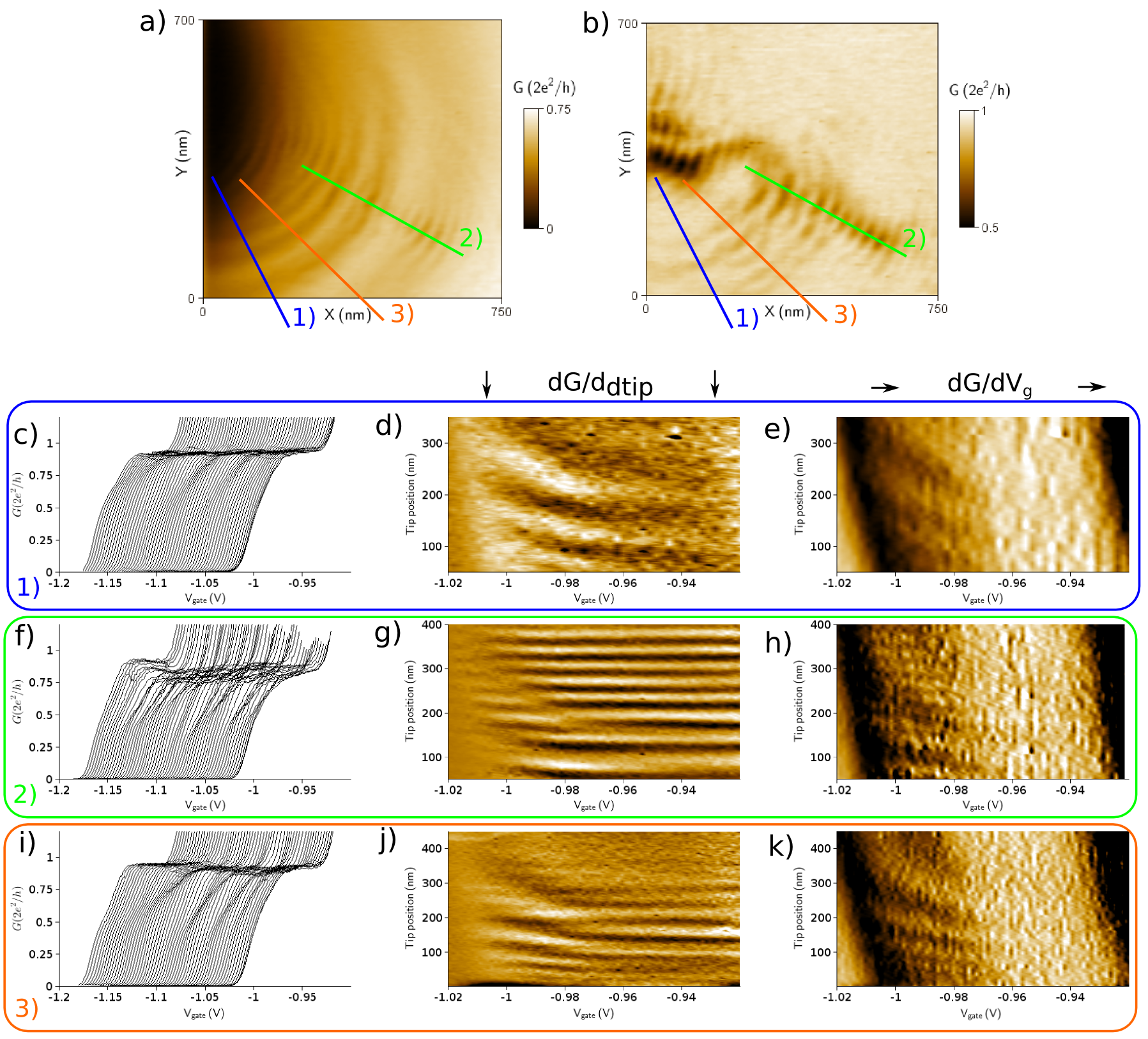
Supplementary Note 1 : Conductance oscillations and interference fringes.
In Supplementary Figure 4, we present three sets of data, showing the conductance versus split-gates voltage and tip position along three different scanning lines, as indicated in Supplementary Figure 4a and 4b. These data are analyzed in different ways: raw data for a set of tip positions, and two color-plots obtained by differentiating the signal with respect to (w.r.t.) either tip position, or gate voltage. As the interferences and the rings do not behave in the same way with respect to these two parameters (tip position and gate voltage), differentiating the signal w.r.t. one or the other of these parameters does not highlight the same details. The chosen line also affects which phenomenon is observed, as interferences are present only in specific regions (i.e. in the branches).
Along the blue line 1, the interferences are almost absent, hence the signal shows only the concentric rings. Supplementary Figure 4c shows that these rings correspond to successive modulations of the 0.7 anomaly. These modulations appear clearly in Supplementary Figure 4d and 4e where the conductance is differentiated w.r.t. and , respectively.
Along the green line 2, the interferences form the main signal. Supplementary Figure 4f shows that these interferences strongly affect the conductance of the plateau, whose value is (in average) below , because of backscattering by the tip located above a branch. Differentiating these data w.r.t. tip position in Supplementary Figure 4g highlights these interferences. However, the ring structure is still present along this line, and differentiating the signal w.r.t. gate voltage in Supplementary Figure 4h recovers signatures of the rings.
Finally, data presented in the paper are shown in Supplementary Figure 4i, corresponding to the orange line 3. As interferences are slightly visible along this line in Supplementary Figure 4b, the signal is a mix between the two behaviors described above. Differentiating the signal w.r.t. tip position in Supplementary Figure 4j gives a rather unclear picture, where interferences and rings are mixed. However, as the interferences do not accumulate much phase with gate voltage, differentiating the signal w.r.t. gate voltage in Supplementary Figure 4k hides these interferences and highlights only the rings structure, which behaves in a very different way.
This analysis shows that differentiating the signal w.r.t. some parameter shall be used really carefully. For this reason, we used this differentiation technique only once in the paper (Fig. 3b), in a demonstrative way to show that the rings structure is contrasted below the first plateau, but not to perform any quantitative analysis.
Supplementary Note 2 : Electrostatic simulation of the QPC electron density.
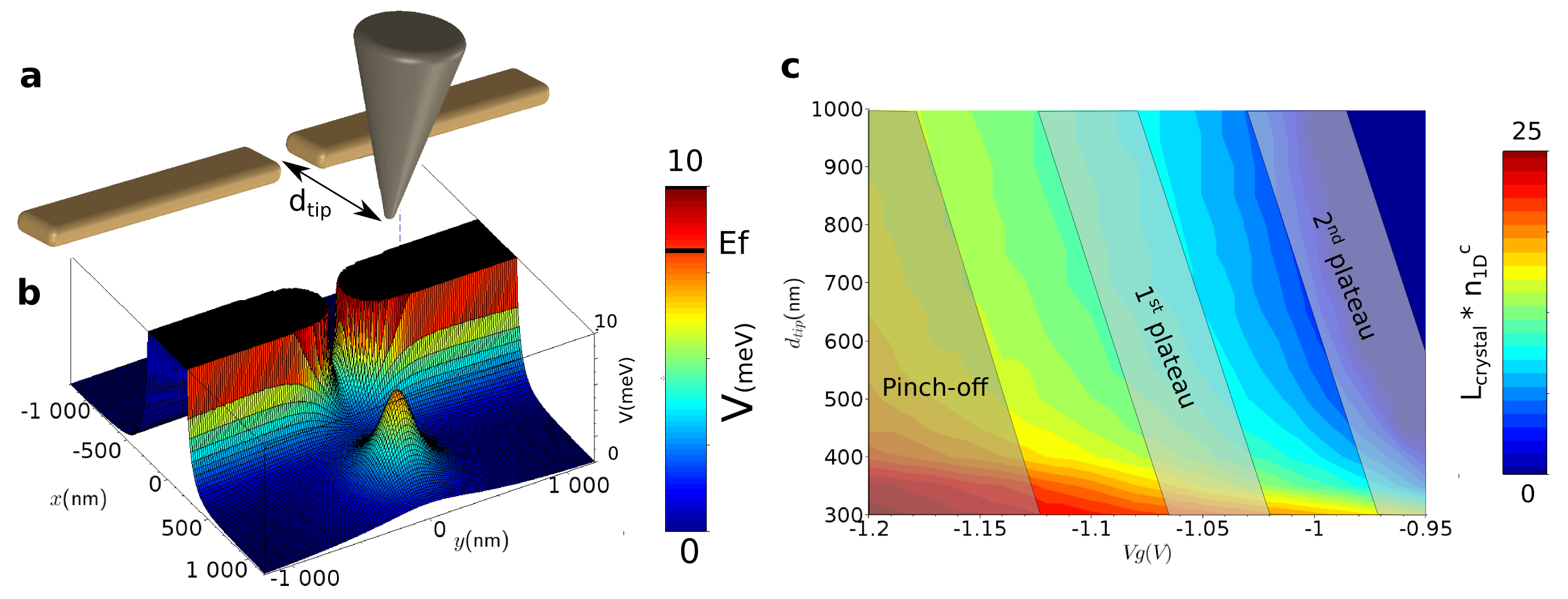
In order to justify that a finite number of charges can localize in the QPC channel, we perform self-consistent classical electrostatic simulations using the Comsol software, as explained in the paper (see Fig. 5 and Methods). We present here additional details and results of these simulations.
We model the system in three dimensions as shown in Supplementary Figure 5a. The metallic gates are 120 nm thick and define a 270 nm wide and 300 nm long constriction, corresponding to our sample geometry. The tip is modelled by a cone with a rounded apex of curvature radius 30 nm. The 2DEG plane is located 105 nm below the surface according to our heterostructure and we define a dielectric constant between the 2DEG and the surface to model GaAs. The doping layer is represented by a uniformly charged plane, with a cm-2 density of ionized dopants, located in the 2DEG plane for stability reasons, and insensitive to the local potential. When no voltage is applied neither on gates nor on the tip, the electron density in the 2DEG is /cm2. For non-zero gate and/or tip voltages, the local electron density and the local electrostatic potential are computed self-consistently by successive iterations. The computation therefore includes screening from the 2DEG.
An example of simulation is presented in Supplementary Figure 5b, showing the self-consistent electrostatic energy in the 2DEG, in presence of the tip located at 800 nm from the QPC. The pinch-off is obtained for a gate voltage of -1.17 V (in absence of the tip), which is close to the experimental value of -1.06 V. The difference may come from the fact that we assume no charges on the surface and that the doping layer is placed in the 2DEG plane rather than 40 nm above. The simulations show that -6 V applied on the tip placed 30 nm above the surface is the threshold value for the depletion of the 2DEG below the tip, which is very consistent with our experiment. Moreover, the rise in the QPC saddle point when the tip is approached by 500 nm is about 800 eV in the simulation, compared to the 850 eV evaluated from Fig. 3b of the paper.
From the self-consistent 2D electron density, we calculate the 1D electron density by integration along the transverse direction. The size of the Wigner crystal formed inside the QPC in the low density region depends on the critical density , whose value is still debated. As an example, we choose the value and calculate the size as explained in the paper, for different tip positions and gate voltages. Assuming in a first approximation that the number of localized charges is proportional to times the density , we plot this number of charges in Supplementary Figure 5c, with respect to gate voltage and tip distance (measured from the QPC centre). The figure also indicates roughly the regions corresponding to the transitions between conductance plateaus. These regions have been tilted by the average cross-talk of the tip on the QPC opening (partially screened by the metallic split-gates) according to the experiment (Fig. 3b).
Supplementary Figure 5c shows that approaching the tip towards the QPC changes the number of localized charges by several units, which is qualitatively consistent with the number of observed oscillations in our experiment. A change by one crystallized charge corresponds experimentally to a switch between a zero-bias peak and finite-bias peaks, i.e. to half a period of the oscillations.
It also shows that, when the tip is far ( nm), the estimated number of localized charges changes by about one unit during the first opening (along the axis). This is consistent with the only splitting of the ZBA visible experimentally at a conductance around in Supplementary Figure 1a.
These results are also consistent with the experimental data reported in Ref. Iqbal-2013-sup . Since increasing the channel length enlarges the crystallization region, the successive ZBA splittings observed in their experiment could also be explained considering Wigner crystallization.
Finally, Supplementary Figure 5c shows that a finite number of charges can localize up to the second plateau, which could explain the “0.7 analogues” often observed in QPCs: a structure similar to the 0.7 anomaly at a conductance value of about . It can also explain data such as those presented in Fig. 1d of Ref. Cronenwett-2002-sup , where a zero-bias peak is visible between the first and second plateaus, and may even present splitting in this range.
References
- (1) Iqbal, M. J. et al. Odd and even Kondo effects from emergent localisation in quantum point contacts., Nature 501, 79-83 (2013).
- (2) Cronenwett, S. M. et al. Low-temperature fate of the 0.7 structure in a point contact: A Kondo-like Correlated State in an Open System. Phys. Rev. Lett. 88, 226805 (2002).