Direct observation of band bending in topological insulator Bi2Se3
Abstract
The surface band bending tunes considerably the surface band structures and transport properties in topological insulators. We present a direct measurement of the band bending on the Bi2Se3 by using the bulk sensitive angular-resolved hard x-ray photospectroscopy (HAXPES). We tracked the depth dependence of the energy shift of Bi and Se core states. We estimate that the band bending extends up to about 20 nm into the bulk with an amplitude of 0.23–0.26 eV, consistent with profiles previously deduced from the binding energies of surface states in this material.
pacs:
79.60.Bm, 03.65.VfTopological insulators (TIs), a new quantum state, are characterized by robust metallic surface states inside the bulk energy gap, which are due to the topology of bulk band structures. Qi and Zhang (2010); Moore (2010); Hasan and Kane (2010); Qi and Zhang (2011) A large amount of efforts were devoted to observe the topological surface states of many TI materials (Yan and Zhang, 2012, and references therein) by surface-sensitive experiments. Specially, Bi2Se3 is one of the most extensively studied TI materials because of its simple Dirac-type surface states and large bulk gap. Zhang et al. (2009); Xia et al. (2009); Chen et al. (2010)
Surface band bending (SBB) effects of Bi2Se3 has been commonly observed in angle-resolved photoemission spectra Hsieh et al. (2009); Chen et al. (2010) (ARPES) and transport measurements Kong et al. (2011); Checkelsky et al. (2011). The SBB is usually caused by surface degrading in ambient environment and surface doping Bianchi et al. (2010); King et al. (2011); Benia et al. (2011); Hsieh et al. (2011), with a downshift of the surface Dirac point, indicating an electron-doped surface Koleini et al. (2013). SBB induces a quantum confinement effect Bahramy et al. (2012) and modifies the surface and bulk bands dramatically. A clear feature of SBB in Bi2Se3 is a pair of Rashba-splitting bands above the Dirac cone. In transport experiments, SBB is also supposed to affect the measurement in a considerable way by directly tuning the bulk and surface charge carrier densities. Steinberg et al. (2010); Checkelsky et al. (2011); Xiu et al. (2011); Kim et al. (2012) So far, this surface band bending has only been deduced Benia et al. (2011); King et al. (2011) from Rashba-splitting of the conduction bands measured by ARPES, that is mainly sensitive to several surface atomic layers, although SBB is predicted to extends in an order of 10 nm distance from the surface into the bulk. A direct measurement of SBB from the surface into the bulk region is yet to be performed.
In this Letter, we reported the direct observation of SBB on the Bi2Se3 surface by HArd X-ray PhotoElectron Spesctroscopy (HAXPES), a bulk sensitive method. The hard x-ray excitation (8keV) produces photoelectrons with high kinetic energy and consequently high inelastic mean free path () resulting in an enhanced probing depth. HAXPES has been successfully utilized in the study of Heusler TIs.Ouardi et al. (2011); Shekhar et al. (2012) The SBB can be directly measured in photoelectron spectroscopy by controlling the escape depth in the photoemission process to track the depth dependence of core level energies. Such controlling can be achieved by changing the photon energy and consequently the inelastic mean free path, as demonstrated by Himpsel et. al Himpsel et al. (1983) for low photon energy regime. The precision of this approach however depends on the energy distribution and the determination of the Fermi edges for different photon energies. Here, we propose the angular resolved HAXPES as an alternative to control the photoelectron escape depth, keeping constant all the experimental parameters: photon energy, incidence angle and probed region. This is possible thanks to the high energy wide-acceptance objective lens setup specially developed for this purpose Matsuda and Daimon (2004); Matsuda et al. (2005). The objective lens enlarge the effective acceptance allowing the measurement of the photoelectron angular distribution with a fixed incident angle. In this work, we measured the angular distribution of the photoemission of Bi2Se3 core levels, from where we observed the electric potential variations from bulk to surface.

Bi2Se3 single crystals were synthesized from stoichiometry mixture of high purity () of bismuth (Bi) and selenium (Se). The elements were sealed in a dry quartz ampoule under a pressure of 10-6 Torr. The sealed ampoule was loaded into a vertical furnace and heated to 800∘C at a rate of 60∘C/hour followed by 12 hours soaking. For a single crystal growth, the temperature was slowly reduced from 800∘C to 500∘C and thereafter by 100∘C/hour to room temperature. This procedure resulted in silver-colored single crystals size of 10 mm.
For HAXPES measurements, the crystal sample was exfoliated and kept in the air for few seconds in order to ensure the saturation of adsorption process at surface, in such a way to eliminate any time-dependent effect. The experiment was performed at BL47XU at Spring-8 (Japan) using 7.94 keV photon energy and -linearly polarized light. The energy and angular distribution of the photoexcited electrons was analyzed using a high energy VG Scienta R4000-HV hemispherical analyzer. The objective lens, set in front of the analyzer, enlarge the effective acceptance angle to about with an angular resolution of . The homogeneity and precision of the system was checked by mapping the angular distribution of Au peaks. The overall energy resolution was about 230 meV. The angle between the electron spectrometer and the photon propagation was fixed at . Incoming photons was set to impinge on the sample at from its surface normal, in such a way that the angular distribution of incoming electrons is measured from -2 to with respect to the sample normal. Sample temperature was kept at 40 K. Figure 1a illustrates how the depth profile of core shift can be extracted from the angular distribution of the photoemission by considering an effective escape depth , being the emission angle. Figure 1b and 1c show the relationship between SBB and the depth dependence of a core level energy shift. The vertical bars in Figure 1c indicate the energy position of the Se peak for different depths. represents the bending amplitude in both figures. The depth dependence of the energy shift of core levels mimics the band bending profile.
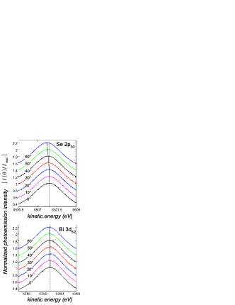
Symbols in Figure 2 represent the experimental energy distribution curves (EDC) for Se 2p3/2 and Bi 3d5/2 core state photoemission. The spectra are summed up over slices of about the photoemission direction indicated by the label on the right of each curve. The curves were normalized by the peak intensity. Direct inspection of the EDC indicates an energy shift in the core level peaks, as represented by the solid curved line. A total shift of -75(1) meV from to for both Se 2p3/2 and Bi 3d5/2 peaks was determined by Voigt function fitting. is calculated by TPP-2M formulaTanuma et al. (1994) to be nm and nm for Bi and Se respectively. Providing the large electron escape depth and kinetic energies, the measured EDC can only be originated by a bent potential which extends from surface up to a distance of the same order of magnitude than . Therefore, the observed shifts indicate that bulk core-levels () have smaller binding energy than core-levels near to the surface (). This remarkable result consists in the direct observation of the band bending in Bi2Se3, indicating a downward bending from bulk to surface.
For a quantitative analysis, we model the angular distribution by the following equation:
| (1) |
where represents the constant background, and is a Lorenztian function. The Lorentzian shape is given by and , representing the background asymmetry and spectral linewidth respectively. The peak is centered in different energies according to the depth position . mimics the band bending (see Figure 1).
| Parameters | Bi 3d5/2 | Se 2p3/2 |
|---|---|---|
| 5359.52 eV | 6507.40 eV | |
| eV | eV | |
The band bending depth profile depends on detailed characteristics of the charge distribution near the surface. As simplest approach we modeled the band bending profile as a quadratic function, extending for a distance from the surface (). This approach allows the evaluation of the extension and strength of the band bending in Bi2Se3 by refining :
| (2) |
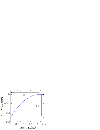
For comparison with the experimental data, the calculated spectra were convoluted with a Gaussian representing the total energy resolution (FWHM=). The curves were refined by the minimization of the mean square error (MSE). The optimized parameters for Se and Bi peaks are summarized in Table I. The optimum values for and are respectively 2.13 (or 2.29) and 0.25 eV. The calculated spectra using optimum parameters are shown in Figure 2 as solid lines. Figure 3 shows the depth dependence of the energy shift of both core levels, as derived from . The axis is shown normalized by the . The uncertainty in the estimation of coefficients was calculated by finding the ranges within the variation of the total MSE from the optimum value is smaller than 1%. It results in the regions: 1.95–2.25 and 0.23–0.26 eV. Therefore, our model suggests that the band banding extends to (about 20 nm). These results are in agreement with the band bending inferred from surface states position in ARPES measurements Benia et al. (2011); King et al. (2011).
In summary, we have observed the band bending Bi2Se3 by measuring the angular dependence of high energy photoelectrons emitted from core levels. The angular dispersions in kinetic energy were modeled as originated from a depth-dependent shift in binding energy of core states. The depth profile of core shifts was extracted in a single experiment from the angular distribution of photoelectrons. We found a downward band bending of about 0.25 eV, which extends to approximately 20 nm into the crystal, in good agreement with the values deduced from ARPES measurements Benia et al. (2011); King et al. (2011). Finally, it should be emphasized that the use of the angle-resolved HAXPES in wide angle allows the deeply probing of bulk states and opens the avenue for investigation of band bending and interface potential in multilayered structures.
This work was financially supported by the Deutsche Forschungsgemeinschaft (DFG, German Research Foundation) within the priority program SPP1666 ”Topological insulators”. The synchrotron radiation measurements were performed at BL-47XU with the approval of the Japan Synchrotron Radiation Research Institute (JASRI) (Proposal No. 2012A0043)
References
- Qi and Zhang (2010) X. Qi and S. Zhang, Physics Today 63, 33 (2010).
- Moore (2010) J. Moore, Nature 464(7286), 194 (2010).
- Hasan and Kane (2010) M. Z. Hasan and C. L. Kane, Rev. Mod. Phys. 82(4), 3045 (2010).
- Qi and Zhang (2011) X.-L. Qi and S.-C. Zhang, Rev. Mod. Phys. 83, 1057 (2011).
- Yan and Zhang (2012) B. Yan and S.-C. Zhang, Rep. Prog. Phys. 75(9), 096501 (2012).
- Zhang et al. (2009) H. Zhang, C.-X. Liu, X.-L. Qi, X. Dai, Z. Fang, and S.-C. Zhang, Nature Phys. 5(6), 438 (2009).
- Xia et al. (2009) Y. Xia, D. Qian, D. Hsieh, L. Wray, A. Pal, H. Lin, A. Bansil, D. Grauer, Y. S. Hor, R. J. Cava, and M. Z. Hasan, Nature Phys. 5(6), 398 (2009).
- Chen et al. (2010) Y. Chen, J. Chu, J. Analytis, Z. Liu, K. Igarashi, H. Kuo, X. Qi, S. Mo, R. Moore, D. Lu, et al., Science 329(5992), 659 (2010).
- Hsieh et al. (2009) D. Hsieh, Y. Xia, D. Qian, L. Wray, J. Dil, F. Meier, J. Osterwalder, L. Patthey, J. Checkelsky, N. Ong, et al., Nature 460(7259), 1101 (2009).
- Kong et al. (2011) D. Kong, J. J. Cha, K. Lai, H. Peng, J. G. Analytis, S. Meister, Y. Chen, H.-J. Zhang, I. R. Fisher, Z.-X. Shen, and Y. Cui, ACS Nano 5(6), 4698 (2011).
- Checkelsky et al. (2011) J. G. Checkelsky, Y. Hor, R. J. Cava, and N. P. Ong, Physical review letters 106(19) (2011).
- Bianchi et al. (2010) M. Bianchi, D. Guan, S. Bao, J. Mi, B. Iversen, P. King, and P. Hofmann, Nature Communications 1(8), 128 (2010).
- King et al. (2011) P. D. C. King, R. C. Hatch, M. Bianchi, R. Ovsyannikov, C. Lupulescu, G. Landolt, B. Slomski, J. H. Dil, D. Guan, J. L. Mi, E. D. L. Rienks, J. Fink, et al., Physical review letters 107(9) (2011).
- Benia et al. (2011) H. M. Benia, C. Lin, K. Kern, and C. R. Ast, Physical review letters 107(17) (2011).
- Hsieh et al. (2011) D. Hsieh, J. W. McIver, D. H. Torchinsky, D. R. Gardner, Y. S. Lee, and N. Gedik, Phys. Rev. Lett. 106(5), 057401 (2011).
- Koleini et al. (2013) M. Koleini, T. Frauenheim, and B. Yan, Physical review letters 110(1) (2013).
- Bahramy et al. (2012) M. S. Bahramy, P. D. C. King, A. de la Torre, J. Chang, M. Shi, L. Patthey, G. Balakrishnan, P. Hofmann, R. Arita, N. Nagaosa, and F. Baumberger, Nature Communications 3, 1159 (2012).
- Steinberg et al. (2010) H. Steinberg, D. R. Gardner, Y. S. Lee, and P. Jarillo-Herrero, Nano Letters 10(12), 5032 (2010).
- Xiu et al. (2011) F. Xiu, L. He, Y. Wang, L. Cheng, L.-T. Chang, M. Lang, G. Huang, X. Kou, Y. Zhou, X. Jiang, Z. Chen, J. Zou, et al., Nature Nanotechnology 6(4), 216 (2011).
- Kim et al. (2012) D. Kim, S. Cho, N. P. Butch, P. Syers, K. Kirshenbaum, S. Adam, J. Paglione, and M. S. Fuhrer, Nature Physics 8(6), 460 (2012).
- Ouardi et al. (2011) S. Ouardi, C. Shekhar, G. H. Fecher, X. Kozina, G. Stryganyuk, C. Felser, S. Ueda, and K. Kobayashi, Appl. Phys. Lett. 98(21), 211901 (2011).
- Shekhar et al. (2012) C. Shekhar, S. Ouardi, G. H. Fecher, A. Kumar Nayak, C. Felser, and E. Ikenaga, Applied Physics Letters 100(25), 252109 (2012).
- Himpsel et al. (1983) F. J. Himpsel, G. Hollinger, and R. A. Pollak, Phys. Rev. B 28, 7014 (1983).
- Matsuda and Daimon (2004) H. Matsuda and H. Daimon, Patent: PCT/jp2004/016602 Japan 208926 (2004).
- Matsuda et al. (2005) H. Matsuda, H. Daimon, M. Kato, and M. Kudo, Phys. Rev. E 71, 066503 (2005).
- Tanuma et al. (1994) S. Tanuma, C. J. Powell, and D. R. Penn, Surface and Interface Analysis 21(3), 165 (1994), ISSN 1096-9918, URL http://dx.doi.org/10.1002/sia.740210302.