Integrated optical waveplates for arbitrary operations
on polarization-encoded single-qubits
Abstract
Integrated photonic technologies applied to quantum optics have recently enabled a wealth of breakthrough experiments in several quantum information areas. Path encoding was initially used to demonstrate operations on single or multiple qubits. However, a polarization encoding approach is often simpler and more effective. Two-qubits integrated logic gates as well as complex interferometric structures have been successfully demonstrated exploiting polarization encoding in femtosecond-laser-written photonic circuits. Still, integrated devices performing single-qubit rotations are missing. Here we demonstrate waveguide-based waveplates, fabricated by femtosecond laser pulses, capable to effectively produce arbitrary single-qubit operations in the polarization encoding. By exploiting these novel components we fabricate and test a compact device for the quantum state tomography of two polarization-entangled photons. The integrated optical waveplates complete the toolbox required for a full manipulation of polarization-encoded qubits on-chip, disclosing new scenarios for integrated quantum computation, sensing and simulation, and possibly finding application also in standard photonic devices.
Photons are ideal carriers of quantum information: faint interactions with the environment make them almost immune to decoherence. In particular, the two levels associated to the polarization degree of freedom are advantageously exploited to encode qubits. In fact, entangled-photon sources are available, and many quantum information protocols and experiments have been developed for this encoding mattle1996dce ; lanyon2010tqc ; ma2012qt143 ; sansoni2012tpb ; ma2012edc ; crespi2013ale ; gundogan2012qsp . To implement arbitrary operations on qubits, or equivalently to achieve universal quantum computation, two kinds of elementary linear logic gates are sufficient knill2001sfe : a two-qubit gate, such as the CNOT gate, and single-qubit rotators. For polarization-encoded photons, two-qubit gates require different spatial modes to interact and are experimentally realized by polarization-dependent beam-splitters. On the other hand, single-qubit operations require an interaction between the two polarization modes belonging to the same spatial mode and are experimentally implemented by optical waveplates.
Proof-of-principle demonstrations of photonic qubits interactions and transformations have been realized by bulk-optics equipment obrien2009pqt ; okamoto2010rkc . However, building more complex networks of logic gates encounters severe size and stability limitations: an integrated-optics approach allows to overcome these limitations and has enabled a growing number of experiments in the recent years politi2009iqp ; politi2009sqf ; obrien2009pqt ; tanzilli2012oge ; crespi2013ale ; spring2013bsp ; broome2013pbs ; tillmann2013ebs ; crespi2013imi . In particular, a waveguide-based architecture able to support polarization-encoded qubits has been recently developed, exploiting the femtosecond laser waveguide writing technology sansoni2010pes . Femtosecond laser writing dellavalle2009mpd exploits non-linear absorption of focused ultrashort pulses to create localized regions with increased refractive index in the volume of dielectric substrates. Translation of the sample at constant speed under the laser beam allows to literally draw three-dimensional waveguiding paths with the desired design. The low birefringence of the fabricated waveguides, when certain irradiation parameters are used, makes them ideal for the propagation of polarization encoded qubits with no loss of coherence sansoni2010pes . Polarization dependent or independent directional couplers have been recently demonstrated by this technology, bringing to the realization of a two-qubit CNOT gate crespi2011ipq , as well as complex interferometric structures for quantum simulation sansoni2012tpb ; crespi2013ale .
As a matter of fact this technological platform is not complete, since single-qubit rotations have not been demonstrated yet in integrated optical devices for polarization encoding. Indeed, integrated waveplates with arbitrary axis direction, which effectively allow one to rotate arbitrarily the polarization state of a propagating photon, have never been reported by femtosecond laser writing. Fernandes et al. showed in recent works fernandes2011flw ; fernandes2012sib that the birefringence of femtosecond-laser-written waveguides can be finely tuned in fused silica substrate and, in particular, they demonstrated highly controlled integrated linear retarders. However, in those works the optical axis of the birefringent waveguides was fixed along the vertical or horizontal direction. Incidentally, one can note that producing integrated waveplates with arbitrary optical axis direction is a challenging task also with other conventional waveguide fabrication technologies, because these components require altering the waveguide symmetry in 3D, which is not easy with planar lithographic techniques dai2012ptf .
In this work, we develop a novel method to fabricate integrated waveguide waveplates with tilted axis, by femtosecond laser writing. As we will show, our method requires an extremely simple experimental apparatus. We prove the potential of this technology to implement arbitrary polarization-qubit rotations by realizing and successfully testing a compact device for quantum state tomography jame01pra of two polarization-entangled photons.
Femtosecond-laser-written waveguides are slightly birefringent (typical values range in ), i.e. they support guided modes with different propagation constants for two orthogonal polarization states. The microscopic causes of this birefringence may be diverse depending on the substrate material and the irradiation conditions: ellipticity of the waveguide cross-section snyder1986ofa , mechanical stresses in the modified regionbhardwaj2004sfl , or laser-induced intrinsic birefringence aligned according to the writing beam polarization bricchi2004fbn . We experimentally verified that in the boro-aluminosilicate glass, which we use to produce integrated quantum photonic circuts sansoni2010pes , the polarization direction of the writing laser beam does not affect the waveguide birefringence. Thus, in this glass, we expect only the first two mechanisms to be effective. In this view the waveguide writing process presents an evident symmetry constraint: considering a Gaussian writing beam, a static modification will have a rotational symmetry with respect to the writing beam direction. Hence, independently of the specific microscopic causes of the birefringence, the optical axis will be parallel to this direction.
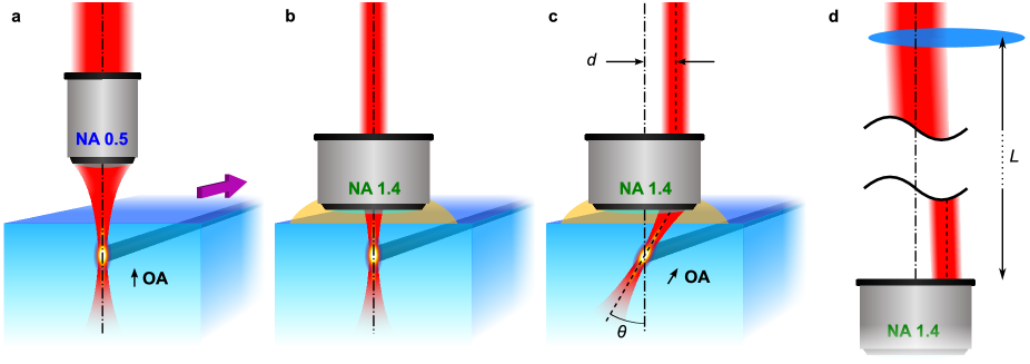
In the vast majority of the waveguide writing experiments reported in the literature, the laser beam direction is orthogonal to the substrate surface and the writing is performed by scanning the beam transversely to its direction (Fig. 1a). The waveguide optical axis is therefore typically orthogonal to the sample surface. According to this discussion, the easiest way to tilt the waveguide optical axis would be to rotate the writing beam of an angle with a rotation axis parallel to the waveguide direction. In this way the waveguide cross-section, together with its optical axis, would rotate of the same angle . However, a macroscopic rotation of the glass with respect to the writing laser beam, or viceversa, would not be a convenient solution. In fact, in order to avoid large translations of the writing beam inside the glass sample at every rotation , a hard-to-obtain resolution in setting the position of the rotation axis would be required. In addition, light refraction at the tilted glass interface would further complicate the fine positioning of the writing focal spot. Finally, the angle-dependent aberrations and Fresnel reflections of the writing beam across the tilted glass interface would make it necessary to re-optimize the laser irradiation parameters for each tilting angle.
We therefore developed a technique to obtain a birefringent waveguide with tilted optical axis without the drawbacks of a macroscopic rotation of the sample with respect to the writing laser beam. Typical waveguide writing is performed with moderate numerical aperture (NA) microscope objectives (e.g. NA = 0.5, Fig. 1a) to achieve the required waveguide size in a single scan. Our new method to tilt the waveguide optical axis is based on a high-NA oil-immersion objective (typical NA=1.4, Fig. 1b) and a writing laser beam with a diameter smaller than the objective aperture. The reduced dimension of the laser beam with respect to the objective aperture is responsible for a reduced effective NA of oil-immersion objective. An optimization of the beam size can yield an effective NA producing the same waveguides one would obtain with the dry, moderate-NA objective (Fig. 1a,b).
If the laser beam impinges upon the center of the objective, the beam propagates (orthogonally to the substrate surface) without changing its direction. If the laser beam impinges on the objective aperture in an off-center way, the focus position is not altered, but the beam propagates in the substrate at an angle that depends on the offset distance on the objective (Fig. 1c). The fabricated waveguide will then have a tilted cross-section, resulting in a rotated optical axis. One can observe that, being the focus position independent from the beam offset at the aperture (which is true for any commercial, aberration-compensated, oil-immersion microscope objective), the position of the fabricated waveguide is in principle always the same, for any angle . In addition, since the objective remains always orthogonal to the substrate surface, the aberrations are well compensated, while the presence of the immersion oil quenches the Fresnel reflections at the glass interface. This means that the pulse energy delivered at the focal spot is always the same for any and no adjustment is required.
Tilting of the writing beam inside the glass requires transversely offsetting the beam before the focusing objective. This could be effectively done with a pair of motorized mirrors. In our setup, however, we implemented a very simple variant, based on a single, long-focal lens mounted on a linear translator (Fig. 1d). The lens, mounted before the focusing objective, has the twofold effect of reducing the beam diameter to achieve the reduced effective NA and, at the same time, to shift the incidence point on the objective aperture by a small transverse translation of the lens. Actually, this is not a pure translation of the beam impinging on the objective, since it also adds an angular deviation. The latter deviation is however very small given the long focal length and the limited objective aperture. A careful analysis showed that the angular deflection introduced by the lens results in a shift in the writing focal point in the order of a few m. This shift is very reproducible and can be easily compensated during the waveguide writing process. Details on the experimental setup can be found in the Methods section and in the Supplementary Information.
| WG n∘ | 1 | 2 | 3 | 4 |
|---|---|---|---|---|
| d | 0.0 mm | 0.26 mm | 0.75 mm | 0.92 mm |
| 0∘ | 10∘ | 16∘ | 27∘ | |
| 1∘ | 9∘ | 15∘ | 25∘ | |
| b | 2.0310-5 | 1.9710-5 | 2.0410-5 | 1.9910-5 |
| Mode size | 7.37.7m2 | 7.47.6m2 | 7.27.5m2 | 7.07.4m2 |
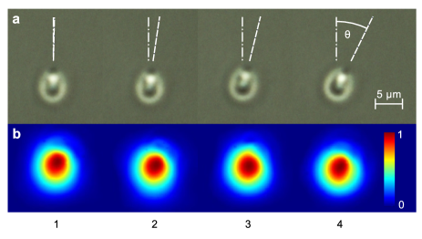
As a first experiment we fabricated several waveguides with different tilt angles, produced by different shifts of the long-focal lens before the focusing objective. For each fabricated waveguide we measured the tilt angle of its cross-section, by acquiring images of the waveguide end-facet with an optical microscope (see Fig. 2a). To fully characterize the waveguide birefringence we measured the Stokes vector of the output polarization state when launching several different input polarization states; we then retrieved the value of birefringence and the optical axis tilt angle that best fitted the experimental data for each waveguide. As shown in Table I, we found a very good agreement between the tilt angle of the cross section, retrieved by the microscope images and the tilt angle of the optical axis determined by the polarization analysis. This confirms our idea that rotating the waveguide cross-section implies a rotation of the optical axis of the same angle. It should be observed that the maximum tilting angle achievable with this technique is limited by the numerical aperture of the microscope objective. In our set-up, with NA=1.4, we achieved rotations of the optical axis up to 32∘ with respect to the vertical axis. In addition, we observe that the birefringence value remains essentially the same at all the different angles with an average . Finally, we measured the near-field profile of the guided mode at 800 nm wavelength for each waveguide (Fig. 2b), noting no relevant differences in the mode size and shape. This confirms that our technique is able to rotate the optical axis with negligible effect on all the other waveguide features. This very important property implies low insertion losses in practical devices, where waveguides with different optical axis direction will be written consecutively.
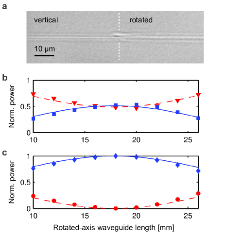
To cascade waveguide segments with different orientations of the optical axis we write the different segments in successive scans. This is made possible by a mechanical shutter synchronized with the motion of the translation stages; the shutter enables the irradiation only in the regions where waveguide segments with a given optical axis tilt have to be fabricated. Then the long-focal lens is translated to a new position and the segments with a different optical axis tilt are produced. Figure 3 shows a microscope top-view image of the junction between two waveguide segments with different optical axis direction; a perfect alignment as well as a hardly noticeable discontinuity can be appreciated. To test our capability to fabricate effective integrated waveplates we realized waveguides comprising two segments, the first with vertical optical axis, the second with optical axis tilted by 22.5∘. Keeping constant the overall length of the waveguide, we varied the length of the two segments. We characterized the devices by injecting horizontally and vertically polarized laser light into the segment with a vertical optical axis and by measuring the projections on the vertical (V), horizontal (H), diagonal (D) and antidiagonal (A) polarization states of the output (see, for example, Fig. 3b and c for H polarized input state projected onto the H/V and D/A bases, respectively). The first waveguide segment has actually no influence on the vertical or horizontal input polarization states, while the second one introduces a polarization rotation. The induced polarization rotations fit very well with the theoretical behaviour calculated for the different lengths of the segment with rotated axis. At a suitable length of about 18 mm of the second segment a clear half-waveplate operation is observed: more than 99% of the incoming H polarized light is converted into D polarization state. Coherently, no light is found in the A state, while an even splitting of light is found in the H/V basis.
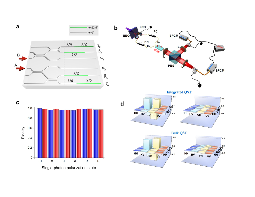
As a probing benchmark of our technology, we fabricated the complex device represented in Fig. 4a, which is an integrated optical analyser of two-photon polarization states. The device is composed of two twin parts, one per each photon (A and B). Each part comprises a network of polarization independent couplers (we employed the three-dimensional architecture devised in Ref. sansoni2012tpb ) that equally split the input light into three arms. The arm consists in a waveguide with vertical birefringence axis. The arm terminates with a waveguide segment operating as a half-waveplate, tilted by 22.5∘ (the remaining segment with tilt 0∘ does not have any effect on the polarization measurement since its optical axis is aligned to the polarizing beam splitter placed at the output, see Fig. 4b). The arm terminates with two consecutive waveguide segments, acting as a vertically oriented quarter waveplate and a half-waveplate tilted by 22.5∘. The polarization rotations induced by the input fibers and by the first part of the integrated device (up to the dashed line in Fig. 4a) are compensated by fiber polarization controllers in each input mode (Fig. 4b). By cascading to this device a single (bulk) polarization beam splitter it is possible to achieve a parallel analysis of the polarization state of the input light in the three basis (vertical and horizontal, diagonal and antidiagonal, right- and left-handed circular polarization). Hence, a complete tomography of one- and two-photon polarization states can be accomplished. Figure 4c,d shows the results of our measurements with single and two-photon states (technical details in the Methods and in the Supplementary Information). In particular, Fig. 4c reports the fidelities of the tomographic measurements on single photon states, with an average value of Figure 4d shows the reconstructed density matrix of a polarization-entangled Bell state, which yields a fidelity to the same measurement performed with a standard bulk-optics quantum state tomography equipment.
In conclusion, we developed a new technique to fabricate waveguide segments acting as integrated waveplates, with precise control of the tilt angle. We demonstrated the capability of our devices to perform arbitrary transformations on the polarization state of light propagating in an integrated waveguide circuit, with both classical and quantum states of light. In particular, an integrated device for on-chip analysis of the polarization state of two entangled photons is provided. The integrated optical waveplate constitutes one of the fundamental components, and the last missing, of an integrated platform aimed at the manipulation of polarization-encoded qubits. The demonstration of this device opens the way to the integration of a broader set of experiments and devices that use photon polarization as the most general degree of freedom for implementing many quantum information processes. In particular, the on-chip control of photon polarization will enable the implementation of on-chip polarization-based quantum metrology mitchell2004srp and, if combined with path encoding, the integrated manipulation of hyperentangled photon states vall09pra .
Methods
Femtosecond laser waveguide writing Our waveguide fabrication setup is based on a regeneratively amplified Yb:based femtosecond laser system (HIGHQLaser FemtoREGEN), with wavelength nm, pulse-duration of 400 fs and 960 kHz repetition rate. The beam is focused by a oil-immersion microscope objective, at 170 m depth below the surface of borosilicate glass substrates (Corning EAGLE 2000). Sample translation at constant speed is provided by Aerotech FiberGLIDE high-precision, air-bearing translation stages. To deflect the laser beam and translate its incidence point on the objective aperture, a spheric lens with focal length cm was used, located at a distance cm from the objective aperture. This allowed us to reduce the laser spot size to a diameter 1.6 mm, which is about 2.8 times smaller than the objective aperture 4.5 mm. The effective numerical aperture approximately scales by the same factor with respect to the full value , reaching an , which is comparable to values commonly employed for femtosecond laser waveguide writing. Optimum single-mode waveguides at 800 nm were fabricated with a pulse energy of 210 nJ and translation speed of 20 mm/s. Propagation losses at 800 nm wavelength have been measured as 0.2 dB/cm. A mechanical shutter (Thorlabs SH05) is used to append different waveguide segments written with different optical axis directions.
Measurements with quantum light Let us refer to Fig. 4b. To perform measurements with quantum light, a -barium borate (BBO) crystal cut for type II phase matching and pumped by a CW diode laser ( 405 nm), generates polarization-entangled photon pairs in the state at 810 nm via spontaneous parametric down conversion kwia95prl . Photon pairs are then delivered to the integrated circuit (QST chip) through single-mode fibers. The output modes of the chip are collected by an aspheric lens (L) and delivered to a bulk polarizing beam splitter (PBS) which transmits horizontal and reflects vertical polarized light. Both the transmitted and the reflected modes are collected by multimode fibers mounted on motorized stages. Photons are then detected by single-photon-counting modules (SPCM), and coincidences between photon pairs are finally recorded.
Birefringence compensation in the quantum state tomography measurements The waveguides constituting the first part of the fabricated device for quantum state tomography are birefringent, and some birefringence is also present unavoidably in the optical fibers used to inject photons in the chip. To compensate for the polarization rotations induced by the propagation in these sections of the circuit (fibers and waveguides) we adopted the following strategy. First, we compensated horizontal and vertical polarization by means of standard polarization controllers (PCs) acting on the input fibers, by injecting horizontally polarized light and measuring the state emerging from the outputs (see Fig. 4a). Second, we adjusted the phase between horizontal and vertical polarizations with a liquid-crystal controllable waveplate (LC), by injecting into the chip diagonal (circular) polarized light and measuring the state emerging from the () outputs.
References
- (1) K. Mattle, H. Weinfurter, P. G. Kwiat, and A. Zeilinger, Dense coding in experimental quantum communication, Phys. Rev. Lett. 76, 4656 (1996).
- (2) B. P. Lanyon, J. D. Whitfield, G. G. Gillett, M. E. Goggin, M. P. Almeida, I. Kassal, J. D. Biamonte, M. Mohseni, B. J. Powell, M. Barbieri, A. Aspuru-Guzik, and A. G. White, Towards quantum chemistry on a quantum computer, Nature Chem. 2, 106 (2010).
- (3) X.-S. Ma, T. Herbst, T. Scheidl, D. Wang, S. Kropatschek, W. Naylor, B. Wittmann, A. Mech, J. Kofler, E. Anisimova, V. Makarov, T. Jennewein, R. Ursin, and A. Zeilinger, Quantum teleportation over 143 kilometres using active feed-forward, Nature 489, 269 (2012).
- (4) L. Sansoni, F. Sciarrino, G. Vallone, P. Mataloni, A. Crespi, R. Ramponi, and R. Osellame, Two-particle bosonic-fermionic quantum walk via integrated photonics, Phys. Rev. Lett. 108, 010502 (2012).
- (5) X.-s. Ma, S. Zotter, J. Kofler, R. Ursin, T. Jennewein, Č. Brukner, and A. Zeilinger, Experimental delayed-choice entanglement swapping, Nature Phys. 8, 480 (2012).
- (6) M. Gündoğan, P. M. Ledingham, A. Almasi, M. Cristiani, and H. de Riedmatten, Quantum storage of a photonic polarization qubit in a solid, Phys. Rev. Lett. 108, 190504 (2012).
- (7) A. Crespi, R. Osellame, R. Ramponi, V. Giovannetti, R. Fazio, L. Sansoni, F. D. Nicola, F. Sciarrino, and P. Mataloni, Anderson localization of entangled photons in an integrated quantum walk, Nature Photon. 7, 322 (2013).
- (8) E. Knill, R. Laflamme, and G. Milburn, A scheme for efficient quantum computation with linear optics, Nature 409, 46 (2001).
- (9) J. O’Brien and J. Akira Furusawa, Photonic quantum technologies, Nature Photon. 3, 687 (2009).
- (10) R. Okamoto, J. L. O’Brien, H. F. Hofmann, and S. Takeuchi, Realization of a Knill-Laflamme-Milburn controlled-not photonic quantum circuit combining effective optical nonlinearities, Proc. Natl. Acad. Sci. USA 108, 10067 (2011).
- (11) S. Tanzilli, A. Martin, F. Kaiser, M. P. De Micheli, O. Alibart, and D. B. Ostrowsky, On the genesis and evolution of integrated quantum optics, Laser & Photon. Rev. 6, 115 (2012).
- (12) J. B. Spring, B. J. Metcalf, P. C. Humphreys, W. S. Kolthammer, X.-M. Jin, M. Barbieri, A. Datta, N. Thomas-Peter, N. K. Langford, D. Kundys, J. C. Gates, B. J. Smith, P. G. R. Smith, and I. A. Walmsley, Boson sampling on a photonic chip, Science 339, 798 (2013).
- (13) M. Broome, A. Fedrizzi, S. Rahimi-Keshari, J. Dove, S. Aaronson, T. C. Ralph, and A. G. White, Photonic boson sampling in a tunable circuit, Science 339, 794 (2013)
- (14) M. Tillmann, B. Dakic, R. Heilmann, S. Nolte, A. Szameit, and P. Walther, Experimental boson sampling, Nature Photon. 7, 540 (2013).
- (15) A. Crespi, R. Osellame, R. Ramponi, D. J. Brod, E. F. Galvao, N. Spagnolo, C. Vitelli, E. Maiorino, P. Mataloni, and F. Sciarrino, Integrated multimode interferometers with arbitrary designs for photonic boson sampling, Nature Photon. 7, 545 (2013).
- (16) A. Politi, J. Matthews, M. Thompson, and J. O’Brien, Integrated quantum photonics, IEEE J. Sel. Top. Quant. Electron. 15, 1673 (2009).
- (17) A. Politi, J. C. F. Matthews, and J. L. O’Brien, Shor’s quantum factoring algorithm on a photonic chip, Science 325, 1221 (2009).
- (18) L. Sansoni, F. Sciarrino, G. Vallone, P. Mataloni, A. Crespi, R. Ramponi, and R. Osellame, Polarization entangled state measurement on a chip, Phys. Rev. Lett. 105, 200503 (2010).
- (19) G. Della Valle, R. Osellame, and P. Laporta, Micromachining of photonic devices by femtosecond laser pulses, J. Opt. A: Pure Appl. Opt. 11, 013001 (2009).
- (20) A. Crespi, R. Ramponi, R. Osellame, L. Sansoni, I. Bongioanni, F. Sciarrino, G. Vallone, and P. Mataloni, Integrated photonic quantum gates for polarization qubits, Nat. Commun. 2, 566 (2011).
- (21) L. A. Fernandes, J. R. Grenier, P. R. Herman, J. S. Aitchison, and P. V. S. Marques, Femtosecond laser writing of waveguide retarders in fused silica for polarization control in optical circuits, Opt. Express 19, 18294 (2011).
- (22) L. A. Fernandes, J. R. Grenier, P. R. Herman, J. S. Aitchison, and P. V. S. Marques, Stress induced birefringence tuning in femtosecond laser fabricated waveguides in fused silica, Opt. Express 20, 24103 (2012).
- (23) D. Dai, J. Bauters, and J. Bowers, Passive technologies for future large-scale photonic integrated circuits on silicon: polarization handling, light non-reciprocity and loss reduction, Light: Science & Applications 1, e1 (2012).
- (24) D. F. V. James, P. G. Kwiat, W. J. Munro, and A. G. White, Measurement of qubits, Phys. Rev. A 64, 052312 (2001).
- (25) A. Snyder and X. Zheng, Optical fibers of arbitrary cross sections, J. Opt. Soc. Am. A 3, 600 (1986).
- (26) V. Bhardwaj, P. Corkum, D. Rayner, C. Hnatovsky, E. Simova, and R. Taylor, Stress in femtosecond-laser-written waveguides in fused silica, Opt. Lett. 29, 1312 (2004).
- (27) E. Bricchi, B. G. Klappauf, and P. G. Kazansky, Form birefringence and negative index change created by femtosecond direct writing in transparent materials, Opt. Lett. 29, 119 (2004).
- (28) M. W. Mitchell, J. S. Lundeen, and A. M. Steinberg, Super-resolving phase measurements with a multiphoton entangled state, Nature 429, 161 (2004).
- (29) G. Vallone, R. Ceccarelli, F. De Martini, and P. Mataloni, Hyperentanglement of two photons in three degrees of freedom, Phys. Rev. A 79, 030301 (2009).
- (30) P. Kwiat, K. Mattle, H. Weinfurter, and A. Zeilinger, New high-intensity source of polarization entangled photon pairs, Phys. Rev. Lett. 75, 4337 (1995).
Acknowledgements
This work was supported by PRIN 2009 (Progetti di Ricerca di Interesse Nazionale 2009), the ERC-Starting Grant 3D-QUEST (3D-Quantum Integrated Optical Simulation; grant agreement no. 307783): http://www.3dquest.eu, QWAD (Quantum Waveguides Applications & Developments), EU-Project CHISTERA-QUASAR