Doping-dependent band structure of LaAlO3/SrTiO3 interfaces by soft x-ray polarization-controlled resonant angle-resolved photoemission
Abstract
Polarization-controlled synchrotron radiation was used to map the electronic structure of buried conducting interfaces of LaAlO3/SrTiO3 in a resonant angle-resolved photoemission experiment. A strong dependence on the light polarization of the Fermi surface and band dispersions is demonstrated, highlighting the distinct Ti orbitals involved in 2D conduction. Samples with different 2D doping levels were prepared and measured by photoemission, revealing different band occupancies and Fermi surface shapes. A direct comparison between the photoemission measurements and advanced first-principle calculations carried out for different -band fillings is presented in conjunction with the 2D carrier concentration obtained from transport measurements.
pacs:
79.60.Jv, 73.20.-r, 31.15.A-Complex-oxide interfaces exhibit a broad spectrum of electronic properties and complex phase diagrams and have thus attracted considerable attention. A particularly interesting example is the appearance of 2-dimensional (2D) conductivity at the interface between the band insulators LaAlO3 (LAO) and SrTiO3 (STO) Ohtomo and Hwang (2004); Reyren et al. (2007); Caviglia et al. (2008) above a critical LAO thickness of 3 unit cells (u.c.) Thiel et al. (2006). As revealed by ab-initio calculations Popovic et al. (2008); Delugas et al. (2011), the mobile electron charge of this 2-dimensional system (2DES) is confined in conduction bands of orbital character extending over a few STO layers from the interface and is thus very different from that of doped STO bulk. However, the detailed characteristics of these conduction bands crucially depend on the amount of carriers present at the interface. It follows that a comparison between observed and calculated electronic properties of the interface only makes sense if referred to the same carrier concentration.
The band structure calculated for 0.5 electrons per u.c. (3.5 e/cm2), that is the value needed to suppress the “polar catastrophe” due to the diverging potential in polar LAO Nakagawa et al. (2006), is often taken as “reference”. In fact, the experimentally determined mobile carrier density in LAO/STO is always much smaller than that. Typical experimental values reported for the 2D-carrier density, , measured by Hall effect at 100 K are between 1013 and 1014 e/cm2 Gariglio et al. (2009). This suggests an important partial charge localization or other charge-compensating mechanisms such as surface passivation or reconstruction Xie et al. (2011); Bristowe et al. (2011).
Direct access to the electronic band structure is a crucial step towards the full understanding of complex-oxide interfaces. Angle-resolved photoemission spectroscopy (ARPES) is a powerful technique which yields a map of photoelectron intensities as a function of their kinetic energies and momentum, revealing the electronic structure in solids. Recent ARPES studies on bare STO surfaces Meevasana et al. (2011); Santander-Syro et al. (2011); Plumb et al. (2013a) have shown the formation of a 2DES which appears to have similar properties to those of the LAO/STO interfacial conducting layer. Photoemission spectroscopy of buried interfaces is more challenging due to the small inelastic electron mean free path in solids, which, over a wide range of photon energies (), is of the order of 1 nm. However, it was shown recently that a combination of soft x-ray photoemission with resonant photoexcitation Kobayashi et al. (2012); Drera et al. (2011); Koitzsch et al. (2011); Cancellieri et al. (2013); Berner et al. (2013) can overcome this limitation. By selecting at the Ti edge, the signal of the Fermi states associated with conducting electrons is greatly enhanced in LAO/STO interfaces. Berner and coworkers Berner et al. (2013) were the first to report on the Fermi surface (FS) of the LAO/STO interface, confirming the strong similarities between bare STO and STO-based heterostructures. Here we report the first photoemission measurements resolved in both angle and photon polarization which are thus capable to distinguish different orbital contributions to the bands and FSs.
We have correlated the FS shape with the number of carriers measured by magnetotransport, investigating samples with different . The FS and band dispersions visible in the photoemission experiment are highly dependent on the incident photon light polarizations and on , suggesting a strong orbital character and different band filling of these heterostructures. The experimental data are complemented by ab-initio results which for the first time describe the detailed evolution of band energies and FS with the charge density present at the interface, in a density range ( e/cm2) consistent with that measured for the investigated samples. This provides an unprecedented, direct comparison of calculated and measured electronic properties at equal doping. Our photoemission band dispersions and theoretical calculations coherently reproduce the orbital decomposition of charges at the given transport-derived carrier density, thus clarifying the exact level electron occupancy in this system. The possible contribution of photocarriers induced by x-ray radiation was investigated and only an insignificant effect on the electronic structure was measured. Details are given in the Supplementary Materials.
LAO thin films were grown by pulsed laser deposition on (001)-oriented TiO2-terminated STO substrates at C in an oxygen pressure of mbar. These “standard” LAO/STO samples have transport properties similar to those reported in Ref. Gariglio et al., 2009, with e/cm2, measured by the Hall effect (SD samples). Samples with lower 2D-carriers densities (LD samples) have been also prepared using a growth temperature of 650 ∘C, as reported in Ref. Caviglia et al., 2010. These latter samples have a e/cm2. A KrF excimer laser ( nm) was used to ablate the sintered targets with a fluence of J/cm2 at a frequency of Hz, leading to a deposition rate of about one unit cell for pulses. After deposition, the oxygen pressure was raised to bar and the temperature maintained at ∘C for one hour, in order to ensure full oxidation Cancellieri et al. (2010). Film growth was monitored in-situ by reflection high-energy electron-diffraction. The critical thickness required to undergo an insulator-to-metal transition was u.c., as reported in Ref. Thiel et al., 2006. Our conducting interfaces had a LAO thickness between and u.c.
For ab-initio calculations we used an advanced variant of density functional theory, i.e., the variational pseudo self-interaction correction (VPSIC) Filippetti et al. (2011) capable of correcting the imperfect description of standard local-density functionals and reproduce the band-gap of oxide-based systems and the band alignment at the LAO/STO interface Delugas et al. (2011). The different carrier density regimes are described starting from the insulating interface (i.e. for LAO thickness smaller than 4 u.c.) and, while keeping the LAO thickness fixed, introducing an increased amount of electron charge in the system, and leaving the system to fully relax to its structural and electronic ground state (in practice mimicking a field-effect-induced charge accumulation). In this way we can monitor the evolution of the electronic properties due to very tiny and well defined changes of electron charge, comparable in magnitude with the Hall-measured values.
The measurements were performed at the soft-x-ray ARPES endstation of the Advanced Resonant Spectroscopies (ADRESS) beamline Strocov et al. (2010) at the Swiss Light Source. The samples were transferred from the deposition chamber ex-situ without further annealing in vacuum. The beamline delivers a high photon flux, exceeding photons/sec/0.01% bandwidth providing excellent statistics of the interface signal, despite its attenuation as the photoelectrons pass through the film layer. Measurements were performed using different light polarizations, switching between -polarized (circular), -polarized (linear vertical), and -polarized (linear horizontal), to excite states of different symmetries relative to the mirror plane. The experimental geometry is shown in Fig. 1(a). The measurement plane (MP) coincides with the (010) mirror plane formed by the sample normal along the [001] and the -X directions. The experiment was performed at K. The combined beamline and analyzer energy resolution was set to around meV for the valence-band spectra.
Following Ref. Cancellieri et al., 2013, was selected at the Ti absorption edge (see Supplementary Materials). We maximized the intensity at the Fermi level () at sufficient energy separation from the Ti core level second order contribution and selected equal to 460.3 eV. We emphasize that no presence of in-gap states could be found in the samples at any (see Supplementary Materials also for results on the related La0.5Sr0.5Al0.5Ti0.5O3/STO heterostructure Reinle-Schmitt et al. (2012)). These in-gap states, measured in bare STO Meevasana et al. (2011); Plumb et al. (2013a) and very recently also in the LAO/STO interface Berner et al. (2013); Plumb et al. (2013b), appear at 1 eV below the Fermi edge, are resonant with Ti3+ valence states, and are mainly due to surface-defects and impurity states related to oxygen vacancies Aiura et al. (2002). These incoherent states are highly photosensitive, displaying an important photodoping effect. Our oxygen-annealed samples show no such contributions from the oxygen vacancies to the 2D electrical conduction, confirmed by the absence of photodoping.
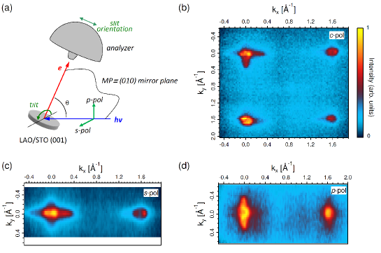
The ARPES data obtained with -polarized photons for a standard LAO/STO sample shown in Fig. 1(b) reveal non-equivalent shapes of the FS in different Brillouin zones, in agreement with Ref. Berner et al., 2013. This behavior can be ascribed to different matrix elements acting on the photoemission intensity from different interface bands, revealing the compound character of the LAO/STO interface states. The linear dichroism of the spectra, shown in Figs. 1(c) and (d), show more clearly and in detail the multiple-state character of these electronic FS components, which are strongly polarization-dependent. The different photon-polarization measurements reveal that the FS is made up of a circle, originating mainly from Ti bands, and two ellipsoids aligned along the and directions, due to the heavy and band contributions. A comparison between the - and -polarized data in Fig. 1 agrees with the orbital character of the FS. The intensity of each band is modulated by the matrix element (photon excitation probability) which depends on the symmetry of the band, the polarization of the incident photons, and their relative angle.
By switching the incident light polarization from - to -polarization, states symmetric and antisymmetric, respectively, with respect to a (010) MP mirror reflection are excited, thereby selecting the different symmetries of the valence states. Thus, with -polarization, only the and states of odd symmetry relative to the MP are detected, while, for -polarized light, only bands with even symmetry with respect to the mirror plane are observed. In Fig. 1(c) (-polarization) the cigar-shaped FS is clearly visible, stretched along the axis, and superimposed on the circular-shaped FS. In Fig. 1(d) (-polarized) only is visible, recognizable by the long side stretched along .
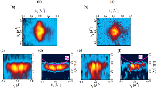
Fig. 2(a)-(f) and Fig. 3(a)-(f) show -polarized and -polarized photoemission data respectively, collected around the point along the -X- direction, for both SD and LD samples. Measurements on a LD sample results in a different band dispersion and FS as shown in Fig. 3(b): the orbitals are almost no longer visible, highlighting the effect of the doping level on the filling of the bands. The different dispersion signals in the intensity plot Figs. 2(a), 3(c) and (e), and shown more clearly in the negative second derivative plots of Figs. 2(b), 3(d) and (f), demonstrate that different bands are enhanced or suppressed by the polarization geometry.
In Fig. 2 are presented the photoemission data acquired with -polarized light. The experimental broadening of the signal at this precludes the possibility of resolving each individual Ti band contributing to the measured photoemission. However, from the photoemission intensity maps, the second derivative plots and the energy-distribution curves (EDCs) in Fig. 2, two types of bands, one lighter and one heavier (the latter having lower intensity, thus not visible in the second Brillouin zones), can be clearly distinguished. Comparison with the VPSIC-calculated symmetries of the bands, superimposed on the photoemission data in Fig. 2(b) and (e), aids recognition of the orbital character of these bands. For the SD sample [Fig. 2(a)] we consider calculation for =6.51013 e/cm2, at this density most of the charge is included in three bands. The lowest two bands have planar orbital characters, effective masses m∗ 0.7 along and Fermi vectors Å-1 and 0.09 Å-1. They collect the electron charge entirely confined within the first and the second TiO2 layer from the interface (see the Supplementary Material for the detailed analysis). The third occupied band has orbital character and includes charges spreading orthogonally to the interface. It is rather flat along (m∗ 9 and Å-1 according to the calculations) and shifted upward in energy by about 70 meV with respect to the most occupied state.
In Fig. 2(e) (LD sample), we superimposed the photoemission intensity maps with bands calculated for =2.61013 e/cm2. Now, is above and empty, thus all the charge is included in the two bands, enclosed in circular Fermi pockets of radius =0.1 Å-1 and 0.06 Å-1. In agreement with the band calculations, the photoemission signal is incompatible with the band.
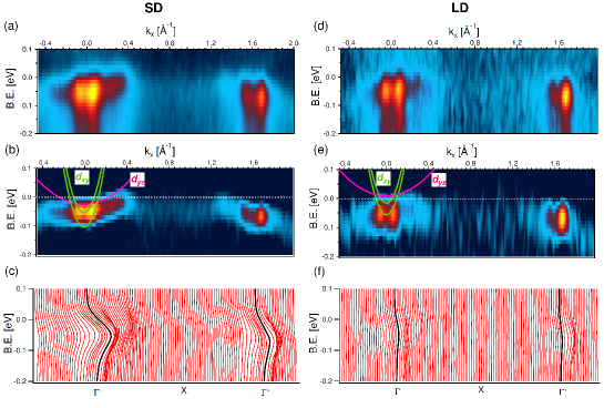
The -polarization results are shown in Fig. 3. By symmetry, only the band are expected to appear, thus here we superimpose only the calculated band [magenta curve in Fig. 3(d) and (f)]. Due to tetragonal symmetry, the band bottom is degenerate with , and its effective mass along is equal to that of along . Thus, for the SD sample, photoemission displays a rather flat band enclosed in a cigar-shaped Fermi pocket of length Å-1, in good agreement with the value 0.23 Å-1 calculated for =6.51013 e/cm2. On the other hand, assuming again =2.61013 e/cm2 for the analysis of the LD sample, the calculated band is completely above . Some admixture shows up in the experiment because of finite acceptance of the analyzer, in the vicinity of the mirror plane.
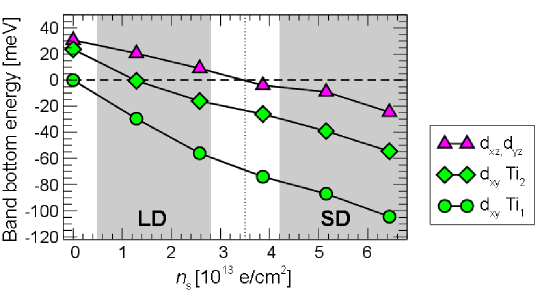
The interpretation of these results can be understood from the band energies’ theoretical evolution as a function of carrier density. First, it is important to realize that, while the in-plane effective masses of the bands are scarcely affected by the interface, their band bottom alignment with respect to , as well as their mutual band splitting, are crucially dependent on the overall amount of mobile charge in the system, as clearly shown in Fig. 4 (a detailed description is presented in the Supplementary Materials). Thus, two samples with substantially different doping may present different charge redistribution in individual orbitals, and in turn radically different photoemission response. At very low density, mobile charge accumulates in the bands closer to the interface [the two bottom energies in Fig. 4 clearly correspond to the green bands shown in Figs. 2(b) and (e)], while orthogonal and orbitals [magenta lines in Figs. 2(b), (e) and 3 (d), (f)] are initially empty. Such a -(,) on-site splitting is a well known consequence of the conduction band misalignment and the suppression of the interface orthogonal hopping. For increasing charge, all bands progressively shift downward in energy across , until, above a certain charge threshold 3.5 1013 e/cm2 (see Fig. 4), a portion of the charge starts to fill the orthogonal (cigar-shaped) orbitals as well. Given the different character of planar and orthogonal orbitals, crossing this threshold represents a dramatic change in optical and transport properties of the 2DES. Our photoemission data for two samples purposely prepared for having doping concentration lower and higher than the theoretically predicted threshold, demonstrates explicitly this regime change. The band bottom energies continue to evolve strongly at increasing carrier concentrations: at e/cm2 corresponding to the half-electron per interface u.c., the (Ti1), (Ti2) and band bottoms are located at -370, -210 and -100 meV, respectively Delugas et al. (2011). These values are clearly incompatible with the experimental observations, demonstrating that the ideal limit dictated by the polarization catastrophe is not achieved in actual samples. These results differ from the ARPES measurements on bare STO - in contrast to the universal 2D FS of bare STO, whose size and shape are decoupled from the bulk sample preparation, it appears that the deposition of LAO with different growth conditions affects the LAO/STO 2D FS size. Moreover our dispersion curves and FSs show that the carriers involved in conductivity have a coherent character and the incoherent part (i.e. in-gap states) is negligible.
In conclusion, we have carried out a polarization-dependent ARPES experiment investigating the symmetry of the valence states and band structure of LAO/STO interfaces. We identify clearly , and bands and directly compare these with ab-initio calculations performed for different band symmetries. Two types of samples have been considered, one having a standard, the other a lower charge density. From first-principles calculations, we have shown that the position of the levels is strongly dependent on the band occupancy. For both samples, ARPES spectra are compatible with the electronic band structures calculated for doping concentrations fixed to the values obtained from Hall measurements, but not with the band structure calculated at the ideal limit of e/u.c. expected in the polar catastrophe scenario. This demonstrates that Hall measurements properly probe the occupancy of the delocalized levels at the interface. This work thus provides benchmark results linking the evolution of the band structure to the sheet carrier density.
Acknowledgements.
The authors are grateful to J.-M. Triscone, S. Gariglio, D. Stornaiuolo and A. Fête for discussion and help in sample preparation. Support of this work by the Schweizerischer Nationalfonds zur Förderung der wissenschaftlichen Forschung, in particular the National Center of Competence in Research, Materials with Novel Electronic Properties, MaNEP. The staff of the Swiss Light Source is gratefully acknowledged. CNR-IOM scientists acknowledge MIUR-PRIN 2010 Oxide, IIT-Seed NEWDFESCM, IIT-SEED POLYPHEMO and “platform computation” of IIT, and Fondazione Banco di Sardegna grants. PhG acknowledges a Research Professorship of the Francqui Foundation and partial financial support from the ARC project TheMoTherm.References
- Ohtomo and Hwang (2004) A. Ohtomo and H. Y. Hwang, Nature 427, 423 (2004).
- Reyren et al. (2007) N. Reyren, S. Thiel, A. D. Caviglia, L. F. Kourkoutis, G. Hammerl, C. Richter, C. W. Schneider, T. Kopp, A.-S. Rüetschi, D. Jaccard, M. Gabay, D. A. Muller, J.-M. Triscone, and J. Mannhart, Science 317, 1196 (2007).
- Caviglia et al. (2008) A. D. Caviglia, N. Gariglio, S Reyren, D. Jaccard, T. Schneider, M. Gabay, S. Thiel, G. Hammerl, J. Mannhart, and J.-M. Triscone, Nature 456, 624 (2008).
- Thiel et al. (2006) S. Thiel, G. Hammerl, A. Schmehl, C. W. Schneider, and J. Mannhart, Science 313, 1942 (2006).
- Popovic et al. (2008) Z. S. Popovic, S. Satpathy, and R. M. Martin, Phys. Rev. Lett. 101, 256801 (2008).
- Delugas et al. (2011) P. Delugas, A. Filippetti, V. Fiorentini, D. I. Bilc, D. Fontaine, and P. Ghosez, Phys. Rev. Lett. 106, 166807 (2011).
- Nakagawa et al. (2006) N. Nakagawa, H. Y. Hwang, and D. A. Muller, Nat. Mater. 5, 204 (2006).
- Gariglio et al. (2009) S. Gariglio, N. Reyren, A. D. Caviglia, and J.-M. Triscone, J. Phys. Condens. Matter 21, 164213 (2009).
- Xie et al. (2011) Y. Xie, Y. Hikita, C. Bell, and H. Y. Hwang, Nat. Commun. 2, 494 (2011).
- Bristowe et al. (2011) N. C. Bristowe, P. B. Littlewood, and E. Artacho, Phys. Rev. B 83, 205405 (2011).
- Meevasana et al. (2011) W. Meevasana, P. D. C. King, R. H. He, S.-K. Mo, M. Hashimoto, A. Tamai, P. Songsiriritthigul, F. Baumberger, and Z.-X. Shen, Nature mat. 10, 114 (2011).
- Santander-Syro et al. (2011) A. F. Santander-Syro, O. Copie, T. Kondo, F. Fortuna, S. Pailhes, R. Weht, X. G. Qiu, F. Bertran, A. Nicolaou, A. Taleb-Ibrahimi, P. Le Fevre, G. Herranz, M. Bibes, N. Reyren, Y. Apertet, P. Lecoeur, A. Barthelemy, and M. J. Rozenberg, Nature 469, 189 (2011).
- Plumb et al. (2013a) N. C. Plumb, M. Salluzzo, E. Razzoli, M. Månsson, M. Falub, J. Krempasky, C. E. Matt, J. Chang, M. Schulte, J. Braun, H. Ebert, J. Minár, B. Delley, K.-J. Zhou, T. Schmitt, M. Shi, J. Mesot, L. Patthey, and M. Radović, ArXiv e-prints (2013a), arXiv:1302.0708 [cond-mat.mtrl-sci] .
- Kobayashi et al. (2012) M. Kobayashi, I. Muneta, T. Schmitt, L. Patthey, S. Ohya, M. Tanaka, M. Oshima, and V. N. Strocov, Appl. Phys. Lett. 101, 242103 (2012).
- Drera et al. (2011) G. Drera, F. Banfi, F. F. Canova, P. Borghetti, L. Sangaletti, F. Bondino, E. Magnano, J. Huijben, M. Huijben, G. Rijnders, and D. H. A. Blank, Appl. Phys. Lett. 98, 052907 (2011).
- Koitzsch et al. (2011) A. Koitzsch, J. Ocker, M. Knupfer, M. C. Dekker, K. Dörr, B. Büchner, and P. Hoffmann, Phys. Rev. B 84, 245121 (2011).
- Cancellieri et al. (2013) C. Cancellieri, M. L. Reinle-Schmitt, M. Kobayashi, V. N. Strocov, T. Schmitt, P. R. Willmott, S. Gariglio, and J.-M. Triscone, Phys. Rev. Lett. 110, 137601 (2013).
- Berner et al. (2013) G. Berner, M. Sing, H. Fujiwara, A. Yasui, Y. Saitoh, A. Yamasaki, Y. Nishitani, A. Sekiyama, N. Pavlenko, T. Kopp, C. Richter, J. Mannhart, S. Suga, and R. Claessen, Phys. Rev. Lett. 110, 247601 (2013).
- Caviglia et al. (2010) A. D. Caviglia, M. Gabay, S. Gariglio, N. Reyren, C. Cancellieri, and J.-M. Triscone, Phys. Rev. Lett. 104, 126803 (2010).
- Cancellieri et al. (2010) C. Cancellieri, N. Reyren, S. Gariglio, A. D. Caviglia, A. Fête, and J.-M. Triscone, Europhys. Lett. 91, 17004 (2010).
- Filippetti et al. (2011) A. Filippetti, C. D. Pemmaraju, S. Sanvito, P. Delugas, D. Puggioni, and V. Fiorentini, Phys. Rev. B 84, 195127 (2011).
- Strocov et al. (2010) V. N. Strocov, T. Schmitt, U. Flechsig, T. Schmidt, A. Imhof, Q. Chen, J. Raabe, R. Betemps, D. Zimoch, J. Krempasky, X. Wang, M. Grioni, A. Piazzalunga, and L. Patthey, J. Synch. Rad. 17, 631 (2010).
- Reinle-Schmitt et al. (2012) M. L. Reinle-Schmitt, C. Cancellieri, D. Li, D. Fontaine, M. Medarde, E. Pomjakushina, C. W. Schneider, S. Gariglio, P. Ghosez, J.-M. Triscone, and P. R. Willmott, Nat. Comm. 3, 932 (2012).
- Plumb et al. (2013b) N. C. Plumb, M. Kobayashi, M. Salluzzo, E. Razzoli, C. Matt, K.-J. Zhou, C. Monney, T. Schmitt, M. Shi, J. Mesot, L. Patthey, and M. Radović, ArXiv e-prints (2013b), arXiv:1304.5948 [cond-mat.mtrl-sci] .
- Aiura et al. (2002) Y. Aiura, I. Hase, H. Bando, T. Yasue, T. Saitoh, and D. Dessau, Surface Science 515, 61 (2002).