Novel Two-dimensional SiC2 Sheet with Full Pentagon Network
Abstract
We propose a promising two-dimensional nano-sheet of SiC2 (SiC2-pentagon) consisting of tetrahedral silicon atoms and triple-linked carbon atoms in a fully-pentagon network. The SiC2-pentagon with buckled configuration is more favorable than its planar counterpart and previously proposed SiC2-silagraphene with tetra-coordinate silicon atoms; and its dynamical stability is confirmed through phonon analyzing. Buckled SiC2-pentagon is an indirect-band-gap semiconductor with a gap of 1.388 eV. However, its one-dimensional nanoribbons can be metals or semiconductors depending on the edge type, shape, and decoration. Finally, we propose a method to produce the buckled SiC2pentagon through chemical exfoliation on the SiC(001)-c SDB surface.
I Introduction
Group 4 elements have versatile stable and metastable phases due to their ability to form sp-, sp2- and sp3-hybridized chemical bonds. Graphene1 , a single layer of sp2-hybridized carbon atoms, is considered as a promising candidate for future nanoelectronics2 ; 3 in views of its unique electronic properties such as super high carrier mobility 4 ; 5 and anomalous quantum hall effect 6 ; 7 derived from its linear energy dispersion 8 ; 9 ; 10 . Silicon is the most fundamental material in traditional electronic industry. Its two-dimensional (2D) allotrope silicene have been theoretically investigated11 ; 12 ; 13 ; 14 ; 15 and fabricated in experiments recently 16 ; 17 ; 18 ; 19 ; 20 ; 21 . Silicene possessing the same crystal lattice as graphene is considered as a powerful competitor for graphene in future nano-electronics due to its many excellent electronic properties. Especially, silicene system possesses relatively stronger spin-orbit coupling (SOC) 15 in comparison with graphene providing us a possible quantum-spin-hall-effect system. Unfortunately, silicene dose not the ground state of silicon. Under ambient condition, sp2-hybridized graphene is more favorable than the three-dimensional (3D) sp3-hybridized diamond and acknowledged as the ground state of carbon but silicon prefers its 3D cubic phase (diamond-structure) than the 2D silicene. Usually, the experimentally produced silicenes prefer sp2-sp3 mixed configuration than the graphene-liked honeycomb lattice. The experimental synthesis of perfect silicene is still a challenge for current technology.
The theoretical predictions of new materials are very important for their discovery. Many novel materials are theoretically predicted before their experimental fabrication, such as silicene11 ; 12 ; 13 ; 14 ; 16 ; 17 ; 18 and graphane 22 ; 23 ; 24 . Theoretically, we can evaluate the probability and the possibility of the existence of a new material through simulating its thermodynamical stability and dynamical stability, respectively. It is also significant to propose and design the potential approaches to synthesize it in experiments. In addition to the pure carbon graphene allotropes and pure silicene, researchers recently proposed many 2D binary compounds of carbon and silicon such as the SiC sheet 25 ; 26 ; 27 ; 28 ; 29 with the same lattice as boron nitride sheet and the SiC2-silagraphene30 with tetra-coordinate silicon atoms.
In present work, using the segment combination method, we propose a promising two-dimensional (2D) nano-sheet of SiC2 (buckled SiC2-pentagon) through combination of tetrahedral silicon atoms and triple-linked carbon atoms in a fully-pentagon networks locating at the four-linked nodes and the three-linked nodes, respectively. The dynamical stability and the electronic structure of the buckled SiC2-pentagon are evaluated by ab initio calculations. We find that the buckled SiC2-pentagon is more favorable one than the previously proposed planar-SiC2-silagraphene and its dynamical stability is confirmed. The electronic properties of the one-dimensional nanoribbons based on the buckled SiC2-pentagon are systematically investigated. Interestingly, we find that SiC2-pentagon nanosheet has the similar structure with the top layers of the -SiC(001)-c() SDB surface 31 . Referring to the successful preparation of graphene by mechanical exfoliation, we propose that SiC2-pentagon nanosheet can be obtained through chemical exfoliation method from the -SiC(001)-c SDB surface.
II Models and Computational Methods
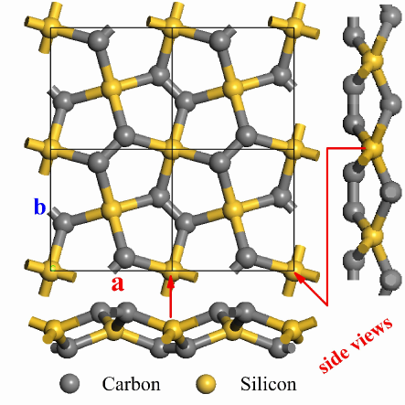
The hexagonal honeycomb-like lattice of graphene and silicene is a fully-hexagon network where every node is equivalent and triple-linked. Based on fully pentagonal network, which contains both four- and triple-linked nodes, we propose a fully-pentagon rule-breaking 2D nanosheet through the combination of the ground states of sp3-hybridized Silicon and sp2-hybridized Carbon locating at the four- and triple-linked nodes, respectively, as shown in 1. Such segment combination method proposed in our previous worksegment has successfully predicted many carbon allotropes based on the most and second stable cubic-diamond and hexagonal-diamond. Both planar and buckled conditions are considered, and the composition ratio of silicon and carbon atoms is 1: 2 . We name them planar-SiC2-pentagon and buckled-SiC2-pentagon, respectively. The previously proposed planar-SiC2-silagraphene30 and its buckled version are also considered in our present work for comparison purpose in views of the fact that they possess the same topological units of four- and triple-linked nodes with the same ration of 1:2. However, SiC2-silagraphenes are topologically different from SiC2-pentagon, SiC2-silagraphene contain both hexagons and rhombuses and SiC2-pentagon contain only pentagons.
To evaluate the stability and electronic structures of SiC2-pentagon, we adopt the Vienna Ab initio Simulation Package (VASP)vasp based on density functional theory (DFT) to perform the first-principles plane-wave calculations for its structural optimizations, total energy calculations, and electronic structures. The projected augmented wave (PAW)paw potentials are chosen to describe the electron-ionic core interaction and the PBE version of the generalized gradient approximation (GGA)gga is adopted for the electronic exchange and correlation. A plane-wave basis set with the kinetic energy cutoff of 500 eV is employed. The Brillouin Zone sample meshes based on the Monkhorst-Pack scheme are set to be denser enough (with k-points separations less than 20.04 Å-1) for all systems to ensure our calculation precision. Lattice constants and atom positions for all systems considered in present work are fully optimized until the residual force on each atom to be less than 0.001 eV/Å. To evaluate the dynamical stability of the 2D SiC2 compounds, we calculate their phonon band structures and phonon density of states (DOS) using the phononphonon package with applying forces from VASP calculations. The energetic stability is evaluated through comparing the cohesive energies.
III Results and discussions
We first introduce the fundamental structural information about these 2D SiC2 sheets. Planar-SiC2-pentagon possesses a tetragonal lattice with constants of
a=b=4.735 Å, c=20Å. It belongs to P4/mbm (127) space group and possesses two inequivalent atomic positions of (0.0, 0.0, 0.5) and (0.6, 0.1, 0.5) for silicon and carbon atoms, respectively. Silicon and carbon atoms are located in the same plane. There are two inequivalent chemical bonds in planar SiC2-pentagon, namely the C-C and Si-C bonds, with length of 1.344 Å and 1.951 Å, respectively. And three inequivalent bond angles are Si-C-Si=118.18∘, Si-C-C=120.91∘, and C-Si-C=90∘, respectively. The buckled-SiC2-pentagon possesses a tetragonal lattice with constants of a=b=4.408 Å, c=20Å. It belongs to P-421m (113) space group and possesses two inequivalent atomic positions of (0.0, 0.0, 0.5) and (0.609, 0.109, 0.533) for silicon and carbon atoms, respectively. Its two inequivalent chemical bonds are the C-C and Si-C bonds with the length of 1.362 Å and 1.908 Å, respectively. Four inequivalent bond angles are Si-C-Si=109.621∘, Si-C-C=117.409∘, intra-sheet C-Si-C=96.9∘ and outer-sheet C-Si-C=139.43∘, respectively. The layer thickness of buckled-SiC2-pentagon is 1.32 Å.
Planar-SiC2-silagraphene possesses an orthorhombic lattice with constants of a=2.809 Å, b=3.925 Å and c=20 Å. It belongs to Pmmm (47) space group and possesses two inequivalent atomic positions of (0.0, 0.0, 0.5) and (0.5, 0.331, 0.5) for silicon and carbon atoms, respectively. The two inequivalent chemical bonds, namly the C-C and Si-C bonds, in planar-SiC2-silagraphene are 1.329 Å and 1.912 Å, respectively. Four inequivalent bond angles are Si-C-Si=94.544∘, Si-C-C=132.73∘, intra-hexagon C-Si-C=94.544∘ and intra-rhombus C-Si-C=85.456∘, respectively. Buckled-SiC2-silagraphene possesses an orthorhombic lattice with constants of a=6.219 Å, b=8.049 Å, and c=20 Å. It belongs to Cmma (67) space group and possesses two inequivalent atomic positions of (0.25, 0.0, 0.5) and (0.5, 0.158, 0.541) for silicon and carbon atoms, respectively. The length of the inequivalent C-C and Si-C bonds in buckled-SiC2-silagraphene are 1.487 Å and 2.170 Å, respectively. Five inequivalent bond angles are Si-C-Si=91.527∘, Si-C-C=125.786∘, intra-hexagon C-Si-C=108.429∘, intra-rhombus C-Si-C=88.473∘, and outer-sheet C-Si-C=135.277∘, respectively. The layer thickness of buckled-SiC2-silagraphene is 1.64 Å. From the analysis of the structural information of those , we can see that the length of the C-C bond in the buckled is larger than that in the planar ones. Moreover, from the point of view of the configuration and bond length of , we can see that carbon atom dose not form a standard sp2-hybridization and silicon atom dose not form a standard sp3-hybridization.
To evaluate the relative stability of these four configurations, we calculate their cohesive energies for each atom as:
| (1) |
Where , , and represent the total energies of the , isolated C atom, and isolated Si atom, respectively. and are the numbers of C and Si atoms, respectively. As shown in 2 (a), we can see that the cohesive energies of the planar SiC2-pantagon, buckled SiC2-pentagon, planar SiC2-silagraphene and buckled SiC2-silagraphene are -5.783 eV/atom, -6.093 eV/atom, -5.885 eV/atom and -6.052 eV/atom, respectively. Although the cohesive energy of the four 2D SiC2 sheets is larger than that of cubic SiC (-6.352), the stability of both buckled SiC2-pentagon and buckled SiC2-silagraphene are more closer to the reference. From the point of view of cohesive energy, buckled SiC2-pentagon is the most stable one in the four 2D SiC2 sheets . The cohesive energy of buckled SiC2-pentagon structure is 0.04eV per atom smaller than that of buckled -silagraphene. Moreover, the results also indicate that silicon prefer the tetrahedral configuration than the tetracoordinate one according to the fact that the buckled structures are more favorable than planar ones.
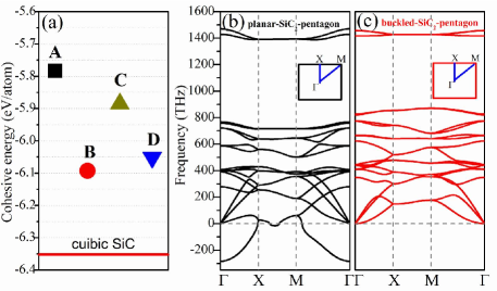
To investigate the dynamic stability of planar-SiC2-pentagon and buckled-SiC2-pentagon systems, we calculate their phonon band structures, as shown in
2 (b) and (c). The phonon spectrum is obtained along the high symmetry direction of the Brillouin zone of the systems with the point of G, X, M. From this picture, we can see that buckled-SiC2-pentagon obviously has no imaginary frequency in the phonon band structures, as shown in 2 (c). Moreover, the phonon density of states (DOS) further confirms such conclusion. The results indicate that the buckled-SiC2-pentagon is dynamically stable. However, the phonon band structures of planar-SiC2-pentagon show imaginary frequency which indicates it is dynamically unstable. We also calculate the phonon band structures of planar-SiC2-silagraphene and buckled-SiC2-silagraphene and the results also show that only buckled-SiC2-silagraphene is dynamically stable. The results indicate that buckled configuration of 2D-SiC2 is more favorable for such systems. The above discussions show that the most promising one among these 2D SiC2 sheets is the buckled-SiC2-pentagon. Then we consider if there is a potential approach to synthesis such a novel nano-material. From the point of view of structure, we find that the lattice constants (a=b=4.408 Å) of buckled-SiC2-pentagon are very close to that of the (100) surface of cubic SiC. Especially, the buckled-SiC2-pentagon has the similar structure with the SiC(001)-c SDB surface31 . If the outermost layers of SiC(001)-c SDB surface can be striped out, it will form buckled-SiC2-pentagon. Such issue will be discussed in detail below.

We then study the electronic properties of the buckled-SiC2-pentagon and its one-dimensional (1D) ramifications. The band structure of the buckled-SiC2-pentagon is shown in 3 (a) and the density of states projected on carbon-atomic-orbits (PDOS-C) and silicon-atomic-orbits (PDOS-Si) are shown in 3 (b) and (c), respectively. The band structures show that buckled-SiC2-pentagon is an indirect-band gap semiconductor with a gap of 1.388 eV. From the PDOSs, we can see that carbon atom dose not form a standard sp2-hybridization and silicon atom dose not form a standard sp3-hybridization due to the mixed existence of the states of px, py, and pz around the valence band maximum (VBM) and conduction band minimum (CBM), which agree well with the above analysis. The formants in both PDOS-C and PDOS-Si show strong interactions between carbon and silicon atoms and the formation of chemical Si-C bonds. Such bonding effect can also be observed from the charge density difference (CDD, defined as the difference between the total charge density in the system and the superpositions of neutral atomic charge densities placed at atomic sites) as shown in 3 (e). The results indicate that the electrons transfer from silicon atoms in tetrahedral sp3-like configuration to carbon atoms in a sp2-like configuration. The corresponding charge densities of the VBM and the CBM are shown in 3 (d) and (f), respectively. We can see the most active valence electrons (VBM electrons) in buckled-SiC2-pentagon mainly distribute on the Si-C chemical bonds. The CBM states mainly distribute on carbon atoms along the direction perpendicular to the sheet indicating that it is mainly contributed by the anti-bonding pz state of carbon. Based on the analysis of PDOSs and the decomposed charge densities we can illustrate the bonding characteristics of buckled-SiC2-pentagon as follows: buckled-SiC2-pentagon contains only -type Si-C bonds and C-C bonds but no -type C-C bonds formed by the pz state electrons of carbon. The pz state electrons of carbon are mixed into -type Si-C bonds. Each -type Si-C bond contains mixed 2s, 2px, 2py and 2pz states of silicon as well as 2s, 2px, 2py, 2pz state electrons of carbon. Each -type C-C bond contains mixed 2s, 2px and 2py electrons of carbon. In view of missing the delocalized -type electrons, buckled-SiC2-pentagon behaves as semiconductor.


Based on the 2D buckled-SiC2-pentagon sheet, we construct four groups of nanoribbons with different edge shapes and hydrogenations, named buckled-SiC2-pentagon-CH, buckled-SiC2-pentagon-CH2, buckled-SiC2-pentagon-SiH, and buckled-SiC2-pentagon-SiH2, as shown in 4 (a), (b), (c) and (d), respectively. Each group contains five nanoribbons with different width (1, 1.5, 2, 2.5 and 3, the definition of the ribbon width is denoted in the figures). 5 (a) shows the Gibbs free energies as functions of ribbon widths for the four groups of nanoribbons. The Gibbs free energy of formation is defined as:gibbs
| (2) |
where is the cohesive energy per atom of the nanoribbon, is the molar fraction of atom () in the structure satisfying , and is the chemical potential of each constituent atoms. We choose as the binding energy per atom of the molecular, and as the cohesive energies per atom of a single layer graphene sheet and cubic silicon, respectively. The results of Gibbs free energy indicate that the 1D derivatives are always more favorable than the 2D buckled-SiC2-pentagon because the 1D derivatives provide enough space to release the inner-sheet strains and reduce the energy of the system. Different ribbons will release different energies depending on their edge types, decorations as well as ribbons widths. We can see that buckled-SiC2-pentagon-SiH and buckled-SiC2-pentagon-SiH2 with silicon termination are always more favorable than buckled-SiC2-pentagon-CH and buckled-SiC2-pentagon-CH2 with carbon termination. Buckled-SiC2-pentagon-SiH and buckled-SiC2-pentagon-SiH2 are even more favorable than the 3D cubic SiC. The Gibbs free energy of buckled-SiC2-pentagon-SiH decrease as the increase in ribbon width, whereas the Gibbs free energy of buckled-SiC2-pentagon-SiH2 increase with the increasing of the ribbon width. As for carbon terminated systems, Gibbs free energy for both buckled-SiC2-pentagon-CH and buckled-SiC2-pentagon-CH2 increases with the increasing of the ribbon width. Moreover, the Gibbs free energy for both buckled-SiC2-pentagon-CH and buckled-SiC2-pentagon-CH2 is higher than that of 3D cubic SiC. The band structures of buckled-SiC2-pentagon-CH, buckled-SiC2-pentagon-CH2, buckled-SiC2-pentagon-SiH, and buckled-SiC2-pentagon-SiH2 are shown in 4. We can see that all of them are semiconductors except for the group of buckled-SiC2-pentagon-CH. Buckled-SiC2-pentagon-CH have similar edge shape and decoration like that of zigzag graphene nanoribbons (ZGNR), they possess similar metallic edge states with those of ZGNRs except for the ultra-narrow one with width of 1, which is a semiconductor with band gap of 0.27 eV. The band gaps of all the 1D ribbons are summarized in 5 (b). We can see that the band gaps of the three semiconducting groups of ribbons distribute in the energy range of 0.76-2.43 eV and approach to 1.46 eV as the increase in the ribbon width. The results of the buckled-SiC2-pentagon nanoribbons indicate that the electronic structures of buckled-SiC2-pentagon can be effectively modulated by patterning them to quasi-one-dimensional materials.
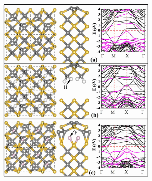
Finally, from the point of view of crystal structure, we find that the buckled-SiC2-pentagon sheet has similar structure with the first three atomic layers of SiC(001)-c SDB surface, as shown in 6 (a). Referring to the successful preparation of graphene by mechanical exfoliation from graphite, we studied the possibility of cleaving the buckled-SiC2-pentagon from the -SiC(001)-c SDB surface through chemical exfoliation method with H/F implantation. Our calculations indicate that the first three atomic layers will spontaneously form the buckled SiC2-pentagon when it is simply cleaved from SiC(001)-c SDB surface into vacuum. To chemically exfoliate the first three atomic layer of the SiC(001)-c SDB surface, we inject H atoms between the third and fourth layer of SiC(001)-c SDB surface, as shown in 6(b). We find that the H atoms tend to bond with the electronegative C atom, such bonding effect induces the Si-C bonds broken between the third and fourth layer of SiC(001)-c SDB surface. Then the first three layers of the SiC(001)-c SDB surface is cleaved from the surface and the layer lifts up to 3Å from the substrate even under equilibrium relaxation calculations. Such cleaved layer is with H saturation which could be reduced under annealing procedure. Besides, we also consider F atoms injecting into the SiC(001)-c SDB surface, as shown in 6 (c). The results show that when the injected F atom concentration is 1/2 layer, it doesn’t form bond with the Si atom at hollow position of the SiC(001)-c SDB surface. However, when doping concentration is 1 layer, F atoms bond to the Si atom at the hollow site of the SiC(001)-c SDB surface, where the F-Si bond length is 1.6 Å and the F-Si-F=78.693∘. The original Si-C bond between the third and fourth layer is borken, and the C atoms of the third layer form new bond with its neighboring Si atom, where all of the C-Si bond length is 2.124 Å which is slightly longer than the bulk Si-C bond length (1.89 Å). Moreover, the C atoms of the third layer not only form bond with the neighboring Si atom, but also form bond with each other with the bond length of 1.495Å, as shown in 6 (c). The configuration of the first three layer is like buckled SiC2-pentagon structure adsorbed on the F decorated SiC(001) surface. The interaction between the first three layer SiC (is also called buckled SiC2-pentagon) and the rest SiC(001)-c SDB surface is greatly reduced by F atoms adsorption. We also calculate the electronic structure of SiC(001)-c SDB surface after the injection of H and F atoms. We can see that the band structures of the first three SiC layers in F-injected configuration close to that of buckled-SiC2-pentagon, as shown in the 5 (c). Our ab initio molecular dynamic (AIMD) simulation under the condition of 273.5 K within NVT shows that such buckled SiC2-pentagon layer can be cleaved from the surface in the first 2 ps of our 10 ps simulation. In real experimental condition, such chemical exfoliation may produce buckled SiC2-pentagon flakes rather than large scale sheet due to the complicated un-controllable procedure of the H/F implantation. We look forward to the synthesis of buckled SiC2-pentagon flakes or even sheet in experiments in the future to confirm our theoretical prediction.
IV Conclusion
Using the segment combination method, we propose a novel two-dimensional nano-sheet of SiC2 (buckled SiC2-pentagon) consisting of tetrahedral silicon atoms
and triple-linked carbon atoms in a fully-pentagon network. With ab initio calculations, we find that the buckled SiC2-pentagon is more favorable than its planar version (planar SiC2-pentagon) and the previously proposed SiC2 silagraphene with tetracoordinate silicon atoms. The buckled SiC2-pentagon is an indirect-band-gap semiconductor with a gap of 1.388 eV and confirmed dynamically stable. Its one-dimensional nanoribbons can be metals or semiconductors depending on the edge types, width, and decorations. Interestingly, the buckled-SiC2-pentagon might be synthesized through chemical exfoliation from SiC(001)-c SDB surface.
Acknowledgements.
This work is supported by the National Natural Science Foundation of China (Grant Nos. 10874143, 11274262, and 11274029 ), the Program for New Century Excellent Talents in University (Grant No. NCET-10-0169), the Natural Science Foundation of Hunan Province (Grant No. 13JJ4046), the Scientific Research Fund of Hunan Provincial Education Department (Grant No. 10K065) .References
- (1) Novoselov, K. S.; Geim, A. K.; Morozov, S. V.; Jiang, D.; Zhang, Y.; Dubonos, S. V.; Grigorieva, I. V.; Firsov, A. A. Science 2004, 306, 666-669.
- (2) Berger, C.; Song, Z.; Li, X.; Wu, X.; Brown, N.; Naud, C.; Mayou, D.; Li, T.; Hass, J.; Marchenkov, A. N. et al. Science 2006, 312, 1191-1196.
- (3) Wang, X.; Li, X.; Zhang, L.; Yoon, Y.; Weber, P. K.; Wang, H.; Guo, J.; Dai, H. Science 2009, 324, 768-771.
- (4) Morozov, S. V.; Novoselov, K. S.; Katsnelson, M. I.; Schedin, F.; Elias, D. C.; Jaszczak J. A.; Geim, A. K. Phys. Rev. Lett. 2008, 100, 016602.
- (5) Bolotin, K. I.; Sikes, K. J.; Jiang, Z.; Fudenberg, G.; Klima, M.; Hone, J.; Kim, P.; Stormer, H. L. Sol. Stat. Commun. 2008, 146, 351-355.
- (6) Nomura, K.; MacDonald, A. H. Phys. Rev. Lett. 2006, 96, 256602.
- (7) Zhang, Y.; Tan, Y.-W.; Stormer H. L.; Kim, P. Nature (London) 2005, 438, 201-204.
- (8) Novoselov, K. S.; Geim, A. K.; Morozov, S. V.; Jiang, D.; Katsnelson, M. I.; Grigorieva, I. V.; Dubonos, S. V.; Firsov, A. A. Nature 2005, 438, 197-200.
- (9) Miao, F.; Wijeratne, S.; Zhang, Y.; Coskun, U. C.; Bao W.; Lau, C. N. Science 2007, 317, 1530-1533.
- (10) Young A. F.; Kim, P. Nat. Phys. 2009, 5, 222-226.
- (11) Takeda, K.; Shiraishi, K.; Phys. Rev. B 1994, 50, 14916.
- (12) Durgun, E.; Tongay, S.; Ciraci, S.; Phys. Rev. B 2005, 72, 075420.
- (13) Guzman-Verri, G. G.; Voon Yan L. C. L.; Phys. Rev. B 2007, 76, 075131.
- (14) Cahangirov, S.; Topsakal, M.; Aktur̈k, E.; Şahin H.; Ciraci, S.; Phys. Rev. Lett. 2009, 102, 236804.
- (15) Liu, C. C.; Feng, W. X.; Yao, Y. G.; Phys. Rev. Lett. 2011, 107, 076802.
- (16) Nakano, H.; Mitsuoka, T.; Harada, M.; Horibuchi, K.; Nozaki, H.; Takahashi, N.; Nonaka, T.; Seno, Y.; Nakamura, H.; Angew. Chem. 2006 118, 6451.
- (17) De Padova, P.; Quaresima, C.; Ottaviani, C.; Sheverdyaeva, P. M.; Moras, P.; Carbone, C.; Topwal, D.; Olivieri, B.; Kara, A.; Oughaddou, H.; Aufray, B.; Le Lay, G.; Appl. Phys. Lett. 2010 96, 261905.
- (18) Aufray, B.; Kara, A.; Vizzini, S.; Oughaddou, H.; Léandri, C.; Ealet, B.; Le Lay, G.; Appl. Phys. Lett. 2010 96, 183102.
- (19) Vogt, P.; De Padova, P.; Quaresima, C.; Avila, J.; Frantzeskakis, E.; Asensio, M. C.; Resta, A.; Ealet, B.; Le Lay, G.; Phys. Rev. Lett. 2012 108, 155501.
- (20) Fleurence, A.; Friedlein, R.; Ozaki, T.; Kawai, H.; Wang, Y.; Yamada-Takamura, Y.; Phys. Rev. Lett. 2012, 108, 245501.
- (21) Chen, L.; Liu, C. C.; Feng, B. J.; He, X. Y.; Cheng, P.; Ding, Z. J.; Meng, S.; Yao, Y. G.; Wu, K. H.; Phys. Rev. Lett. 2012, 109, 056804.
- (22) Sluiter, M. H. F.; Kawazoe, Y.; Phys. Rev. B. 2003, 68, 085410.
- (23) He, C. Y.; Zhang, C. X.; Sun, L. Z.; Jiao, N.; Zhang, K. W.; Zhong, J. X, Phys. Status Solidi RRL 2012, 6, 427.
- (24) Elias, D. C. et al.; Science 2009, 323, 610.
- (25) Menon, M.; Richter, E.; Andriotis, A. N.; Phys. Rev. B 2004, 69, 115322.
- (26) Baumeier, B.; Krug̈er, P.; Pollmann, J.; Phys. Rev. B 2007, 76, 085407.
- (27) Sun, L. A.; Li, Y. F.; Li, Z. Y.; Li, Q. X.; Zhou, Z.; Chen, Z. F.; Yang, J. L.; Hou, J. G.; J. Chem. Phys. 2008, 129, 174114.
- (28) Şahin H.; Cahangirov, S.; Topsakal, M.; Bearoglu, E.; Akturk, E.; Senger, R. T.; Ciraci, S.; Phys. Rev. B 2009, 80, 155453.
- (29) Bearoglu, E.; Topsakal, M.; Cahangirov, S.; Ciraci, S.; Phys. Rev. B 2010, 81, 075433.
- (30) Li, Y. F.; Li, F. Y.; Zhou, Z.; Chen, Z. F.; J. Am. Chem. Soc. 2010, 133, 900.
- (31) Pollman, J.; Krgr, P.; J. Phys. Condens. Matter. 2004, 16, S1659-S1703.
- (32) C He, LZ Sun, J Zhong, J. Superhard Mater. 2012, 34, 386.
- (33) Kresse, G.; Furthmüller, J. Phys. Rev. B 1996 54, 11169. Kresse, G.; Furthmüller, J. Comput. Mater. Sci. 1996, 6, 15.
- (34) Blöchl, P. E. Phys. Rev. B 1994 50, 17953. Kresse, G.; Joubert, D. Phys. Rev. B 1999 59, 1758.
- (35) Perdew, J. P.; Burke, K.; Ernzerhof, M. Phys. Rev. Lett. 1996, 77,3865.
- (36) Parlinski, K.; Li, Z. Q.; Kawazoe, Y.; Phys. Rev. Lett. 1997, 78 4063.
- (37) Hod, O.; Barone, V.; Peralta, J. E.; Scuseria, G. E.; Nano Lett. 2007, 7, 2295.