Current-biased Andreev interferometer
Abstract
We theoretically investigate the behavior of Andreev interferometers with three superconducting electrodes in the current-biased regime. Our analysis allows to predict a number of interesting features of such devices, such as both hysteretic and non-hysteretic behavior, negative magnetoresistance and two different sets of singularities of the differential resistance at subgap voltages. In the non-hysteretic regime we find a pronounced voltage modulation with the magnetic flux which can be used for improving sensitivity of Andreev interferometers.
pacs:
74.45.+c, 74.50.+r, 85.25.AmI Introduction
It was demonstrated experimentally by Petrashov and co-workers Petr1 that the resistance of mesoscopic diffusive normal-superconducting (NS) hybrid structures can be quite strongly modulated by an externally applied magnetic field. These observations open a possibility to construct the so-called Andreev interferometers which – for a number of applications – may have several important advantages over the well known Superconducting Quantum Interference Devices (SQUIDs). Such kind of applications include, e.g., read-out of superconducting qubitsPetrreadout or experimental analysis of switching dynamics of individual magnetic nanoparticlesPetrdynam and require such features of a detecting device as reduced intrinsic dissipation (down to fW level), the possibility to achieve higher sensitivity and read-out speed as well a broad choice of normal conductors employed as a weak link.
Recently, there were both experimental MM and theoretical GT ; GZK investigations of hybrid NS structures with pronounced dependencies of their resistance on the applied magnetic flux. Contrary to the initial design of Andreev interferometers pioneered by Petrashov and co-authors Petr1 , this latest analysis focuses on systems with all external electrodes in the superconducting state. In this way one would be able to reduce dissipation. Current (voltage) harmonics would be generated in this case, which are multiples of the Josephson frequency. However, they can be filtered out and the average current (voltage) can be measured which should reveal a dependence on the magnetic flux.
In Ref. GZK, we already carried out a detailed theoretical analysis of Andreev interferometers in the voltage-biased regime. While this regime can be realized in some experiments, of a clear experimental interest is also another physical situation when the system is biased by a fixed external current. The main purpose of the present work is to analyze the behavior of Andreev interferometers in the current-biased regime.
Note that the system behavior in the latter regime can be very different from that in the voltage-biased one. In a vast majority of normal structures these differences mainly concern higher cumulants of voltage and current. For instance, a decade ago there arose a conundrum caused by experiments Reul , where the third voltage cumulant of the current-biased normal junction was measured. The behavior of this quantity was essentially different from theoretical expectations based on the linear relation between the third voltage correlator in the current-biased regime and the third current correlator Levitov2 ; 3rdcum ; Salo in the voltage-biased regime. This conundrum was resolved in Ref. Kind, which major conclusion was that current and voltage correlators of order three and higher are no longer linearly related.
In superconducting circuits essential differences between the voltage- and current-biased regimes occur already at the level of curves. Such differences were encountered, e.g., in the case of single Josephson junctions McD (see also Ref. Likh, ). The experiments Niem conformed to the corresponding theoretical predictions. Another example is the low temperature behavior of Josephson junction arrays and chains which may vary from superconducting to insulating depending on whether the voltage- or current-biased scheme is considered BFSZ .
The structure of our paper is as follows. In Sec. II we describe the model for Andreev interferometers under consideration. In Sec. III we proceed with theoretical analysis of our model and derive the basic formula that fixes the current-phase relation for our device. This formula is then employed in Sec. IV where we numerically evaluate the curve for our system in the current-biased regime and study the effect of voltage modulation by an external magnetic flux. The paper is concluded by a brief discussion of our key observations in Sec. V. Some technical details are relegated to Appendix.
II The Model
The system under consideration is schematically depicted in Fig. 1. It consists of three superconducting electrodes characterized by the absolute value of the order parameter and a disordered normal metal insertion embedded between these electrodes. A typical size of this normal metallic dot is assumed not to exceed the superconducting coherence length and at the same time to be larger than the elastic mean free path . Two superconducting electrodes 2 and 3 form a loop which is pierced by an external magnetic flux . Accordingly, the superconducting phase difference is induced between the electrodes 2 and 3, where is the superconducting flux quantum.
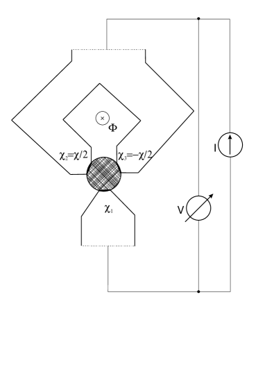
In what follows we will generally assume that all interfaces between the normal metal and superconducting electrodes are weakly transmitting. In this case one can expect to observe a pronounced magnetoresistance modulation effect GWZ . For comparison, in the limit of highly transparent NS interfaces this modulation is expected to remain below ten percent NazSt ; GWZ . The normal state conductances , and between three electrodes and the normal insertion obey the condition
| (1) |
where the normal state resistance is determined by the standard Landauer formula
| (2) |
are the transmissions of conducting channels in the first barrier, is the Drude conductivity of the normal metal, denotes a typical contact area between the normal metal and the electrode, is the diffusion coefficient and is the density of states at the Fermi-surface per spin direction. The electron charge will be denoted by .
Eq. (1) assures that the voltage drop occurs only across the tunnel barrier between the first electrode and the rest of our system. The second inequality (1) also guarantees that our results will not depend on the particular shape of the normal metal insertion. In addition, we will disregard charging effects which amounts to assuming that all relevant effective charging energies remain much smaller than other important energy scales in our problem SZ .
As we already discussed, below we will be interested in the current-biased regime, i.e. we will assume that our system is biased by an external current source , as it is indicated in Fig. 1. Restricting ourselves to this regime we will evaluate the time-averaged voltage across our device which should depend both on the bias current and on the external flux (or, equivalently, on the phase difference ). In the case of Josephson junctions with normal state resistance and capacitance it was demonstrated McD that the curves in the current- and voltage-biased regimes differ substantially provided the parameter remains smaller than one. Below we will also stick to the same limit .
III Current-phase relations
The first step to derive the current-voltage characteristics is to establish the dependence of the instantaneous current value on the phase difference across the NS interface with the smallest conductance . This phase difference is defined by the standard relation
| (3) |
where is the time dependent voltage drop across this NS interface. In order to accomplish this goal one can employ the effective action analysis SZ ; Z94 ; Sny . The general Keldysh effective action describing electron transport across the barrier between the first superconducting electrode and the rest of our structure has the form
| (4) |
Here is the Green-Keldysh matrix of the superconducting reservoir 1 and is the Green-Keldysh matrix of a disordered normal metal which also acquires superconducting properties due to the contact with the reservoirs 2 and 3.
The effective action (4) holds for arbitrary transmission values and allows for a complete description of electron transport through our device. It is convenient to combine the phase variables on the two branches of the Keldysh contour and define the ”classical” () and ”quantum” () components of the phase. Taking the derivatives of the effective action with respect to the quantum phase one can derive the expressions for all current correlators in our problem. Provided charging effects are weak the action (4) can be expanded in powers of and reduced to a much simpler form convenient for practical calculations. In the case of NS hybrid structures this procedure was described in details in Ref. GZ10, .
Since here we are merely interested in the tunneling limit , it suffices to expand the action (4) up to the first order in . Then taking the first variation of the action with respect to one arrives at the current-phase relation in the form
| (5) |
The kernels and are expressed respectively via normal and anomalous components of the Green-Keldysh matrices, i.e.
| (6) | |||
Note that Eqs. (5), (6) can also be derived by means of the standard tunneling Hamiltonian approach.
What remains is to define the Green functions of both the superconducting electrode and the normal metal dot. Without any loss of generality one can set the electric potential of the first superconducting electrode equal to zero. Then the Fourier transforms of and take the form
| (7) |
In order to properly account for the analytic properties of the functions it is important to keep an infinitesimally small imaginary part , i.e.
| (8) |
As the cut in the complex plane goes from to , we obtain for and for .
The Keldysh components and are related to the above retarded and advanced reen functions in the standard manner as
| (9) | |||
Now let us turn to the Green-Keldysh functions of the metallic dot and . These functions have already been evaluated elsewhere BSW ; GZK , therefore here we only briefly recapitulate the corresponding results. It is important to bear in mind that due to the contact with superconducting terminals 2 and 3 the normal metal also acquires superconducting properties. For instance, the proximity-induced minigap in its spectrum develops. This minigap is defined by the equation GZK
| (10) |
where the quantity
| (11) |
depends on the external magnetic flux via the phase difference . The parameter BSW effectively controls the strength of electron-hole dephasing in our system. This parameter is defined as
| (12) |
where stands for the volume of the normal metal.
In order to correctly determine analytic properties of the Green functions we observe that the structure of the cuts in the complex plane is somewhat more complicated. Namely these cuts are now located at , and . As above, the retarded Green functions are defined on the upper banks of these cuts. Provided we find
| (13) | |||
For the remaining values of the retarded Green functions are obtained by analytic continuation with the mentioned cuts, while advanced Green functions are defined as and . Finally, the Keldysh components are again given by Eqs. (9).
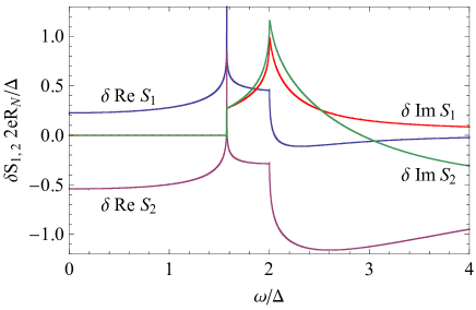
Combining the above expressions for the Green functions with Eqs. (6) it is easy to verify that , i.e. both kernels (6) obey the requirement of causality. In the case of a Josephson junction between two BCS superconductors with different values of the gap the kernels were derived by Werthamer W and also by Larkin and Ovchinnikov LO . For reference purposes the corresponding expressions (denoted below as ) are presented in Appendix. In our case the kernels deviate from since the energy spectrum of the central metallic dot is different from that of a superconductor. The difference
| (14) |
can be evaluated both numerically avail and analytically in some limits. For illustration, in Fig. 2 we display the functions calculated at , and .
Within the logarithmic accuracy an asymptotic behavior of at is described as
| (15) |
where and
| (16) |
These expressions imply modifications in the so-called Riedel singularity Ried as compared to the case of usual Josephson junctions between two superconductors. This difference is by no means surprising since the density of states in our metallic dot differs from that of a BCS superconductor. We also observe that the functions experience a jump at . The magnitude of this jump reads
| (17) |
Finally, we note the presence of peculiarities in the behavior of the functions and at , cf. Fig. 2.
IV Numerical analysis
Our numerical procedure follows closely that of Ref. McD, . We will make use of the representation
| (18) |
where is the average voltage across the tunnel barrier, is the Josephson frequency and are complex numbers to be determined. As usually, Eq. (18) demonstrates that harmonics with higher Josephson frequencies are excited in our device.
Our numerics shows that sufficient accuracy is achieved if one restricts the summation in Eq. (18) by . The numbers are determined bearing in mind that:
(a) In the current biased regime considered here only the component of the current differs from zero,
(b) The condition imposes extra restrictions on and
(c) Here we choose , which is equivalent to .
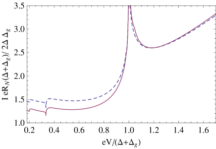
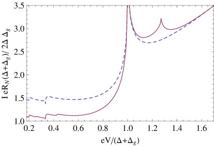
This set of conditions provides real equations sufficient to fully determine . Resolving these equations by the Newton’s method we finally recover the current through our system as a function of the average voltage . The results of numerical analysis are displayed in Figs. 3–5.
Similarly to ordinary Josephson junctions between two BCS superconductors McD ; Likh the curves demonstrate peculiarities at voltage values
| (19) |
where is an integer number. These peculiarities stem from the Riedel-like singularity contained in the kernels . In addition, we also observe extra peculiarities which occur at voltages
| (20) |
These latter features are not present in ordinary Josephson junctions at all. In our case these peculiarities are caused by the behavior of kernels at , see Fig. 2. These additional features on the curve are more pronounced for intermediate values of the electron-hole dephasing parameter and become considerably less pronounced both at small and large values of , cf. Fig. 4 with Figs. 3 and 5.
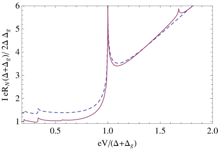
The dependencies presented in Figs. 3–5 demonstrate that at certain values of the bias current the average voltage becomes multivalued, i.e. there exist more that one different voltage states corresponding to the same bias . Accordingly, in this regime one can expect to observe jumps between different voltage branches as well a hysteretic behavior of our device. On the other hand, there also exists a subgap voltage regime where remains single valued for a fixed bias current. For example, for the parameters employed in Figs. 3-5 such non-hysteretic regime is realized within the voltage interval
| (21) |
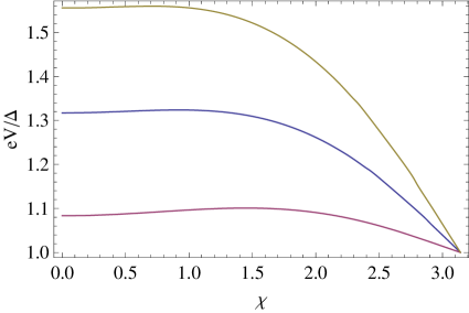
which can be conveniently used, e.g, to perform magnetoresistance experiments. An example of the voltage-phase dependence obtained in this region is presented in Fig. 6. These plots demonstrate negative magnetoresistance, i.e. the system resistance decreases with increasing magnetic flux . The amplitude of this voltage modulation effect decreases with increasing dephasing parameter . Also for the values of sufficiently close to the hysteretic behavior can be reinstated. E.g. for plots displayed in Fig. 6 this is the case at .
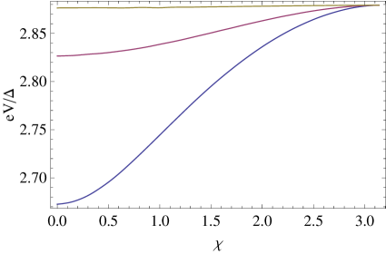
Note that the effect of voltage modulation by the external flux persists also at higher voltages , in which case deviations from the normal state behavior become smaller. In this regime the system magnetoresistance turns out to be positive, though the amplitude of voltage modulations is diminished and becomes vanishingly small for sufficiently large values of . This behavior is exemplified in Fig. 7.
V Discussion
In this work we analyzed the behavior of Andreev interferometer in the current-biased regime. As compared to the voltage-biased regime studied before GZK , we discover a rather different form of the curves and observe some peculiarities, e.g., at voltage values defined in Eqs. (19) and (20). Singularities at voltages (19) are due to the Riedel-like feature and are qualitatively similar to those observed in experiments with ordinary Josephson junctions Niem . Additional features at voltages (20) are specific to systems under consideration and are not present, e.g., in tunnel junctions between two BCS superconductors.
An experimental observation of the above two series of singularities in Andreev interferometers under consideration would be highly interesting as, for instance, it would allow to accurately determine the parameters of such devices. Indeed, the dephasing parameter can be determined with the aid of Eq. (10), e.g., by setting an external magnetic flux equal to zero (and, hence, ). Having established this parameter one can also verify the flux dependence (11) at all values of and also obtain extra information about the conductances and .
Depending on the value of the applied external current Andreev interferometers can show either hysteretic or non-hysteretic behavior. The latter behavior is well suited to study the effect of voltage modulation by an external magnetic flux. E.g. within the voltage interval (21) one observes negative magnetoresistance and significant voltage modulation effect (cf. Fig. 6) which is sufficient for reliable performance of Andreev interferometers.
Let us also note that the above features of Andreev interferometers predicted here, such as hysteretic behavior, peaks in the differential resistance and negative magnetoresistance have been observed in recent experiments Petrnew . It appears, however, that more work will be needed in order to perform a quantitative comparison between theory and experiment.
To complete our discussion we briefly address the effect of voltage noise. Denoting the voltage fluctuation by , introducing the voltage-voltage correlation function
| (22) |
and following the analysis developed in Ref. Zor, for the case of ordinary Josephson junctions (see also Ref. Likh, ), in the limit of low frequencies for we arrive at an estimate
| (23) |
We note that within voltage interval (21) the differential resistance of our device obeys the inequality , see Figs. 3-5. Since the voltage modulation for small is , see Fig. 6, a typical Noise-to-Signal-Ratio (NSR) of our device can be estimated as
| (24) |
Here is the quantum resistance unit and defines the bandwidth for our system. As here we are interested in the averaged voltage and as higher Josephson harmonics should be effectively filtered out, we may set . In addition, we will assume that . In this case the estimate (24) yields . Perhaps, we may also add that, as it was concluded in recent experiments MM ; Petrnew , intrinsic noise of Andreev interferometers was lower than that in employed readout electronics. This observation combined with the estimate (24) appears to indicate that voltage noise may remain sufficiently weak and will not compromise the performance of Andreev interferometers.
Acknowledgements
We appreciate valuable discussions with V.T. Petrashov and J. Pekola. The work was supported by the Act 220 of the Russian Government (project 25).
Appendix A
References
- (1) V.T. Petrashov, V.N. Antonov, P. Delsing, and T. Claeson, Phys. Rev. Lett. 70, 347 (1993); JETP Lett. 60, 589 (1994); Phys. Rev. Lett. 74, 5268 (1995).
- (2) V.T. Petrashov, K.G. Chua, K.M. Marshall, R.Sh. Shaikhaidarov, and J.T. Nicholls, Phys. Rev. Lett. 95, 147001 (2005).
- (3) I. Sosnin, H. Cho, V.T. Petrashov, and A.F. Volkov, Phys. Rev. Lett. 96, 157002 (2006).
- (4) M. Meschke, J.T. Peltonen, J.P. Pekola, and F. Giazotto, Phys. Rev. B 84, 214514 (2011).
- (5) F. Giazotto and F. Taddei, Phys. Rev. B 84, 214502 (2011).
- (6) A.V. Galaktionov, A.D. Zaikin, and L.S. Kuzmin, Phys. Rev. B 85, 224523 (2012).
- (7) B. Reulet, J. Senzier, and D.E. Prober, Phys. Rev. Lett. 91, 196601 (2003).
- (8) L.S. Levitov and M. Reznikov, Phys. Rev. B 70, 115305 (2004).
- (9) A.V. Galaktionov, D.S. Golubev, and A.D. Zaikin, Phys. Rev. B 68, 235333 (2003).
- (10) J. Salo, F.W.J. Hekking, and J. Pekola, Phys. Rev. B 74, 125427 (2006).
- (11) M. Kindermann, Yu.V. Nazarov, and C.W.J. Beenakker, Phys. Rev. B 69, 035336 (2004).
- (12) D.G. McDonald, E.G. Johnson, and R.E. Harris, Phys. Rev. B 13, 1028 (1976).
- (13) K.K. Likharev, Dynamics of Josephson Junctions and Circuits (Gordon and Breach Science Publishers, Amsterdam, 1986).
- (14) J. Niemeyer and V. Kose, Appl. Phys. Lett. 29, 380 (1976).
- (15) P. Bobbert, R. Fazio, G. Schön, and A.D. Zaikin, Phys. Rev. B 45, 2294 (1992).
- (16) A.A. Golubov, F.K. Wilhelm, and A.D. Zaikin, Phys. Rev. B 55, 1123 (1997).
- (17) Yu.V. Nazarov and T.H. Stoof, Phys. Rev. Lett. 76, 823 (1996).
- (18) G. Schön and A.D. Zaikin, Phys. Rep. 198, 237 (1990).
- (19) A.D. Zaikin, Physica B 203, 255 (1994).
- (20) I. Snyman and Yu.V. Nazarov, Phys. Rev. B 77, 165118 (2008).
- (21) A.V. Galaktionov and A.D. Zaikin, Phys. Rev. B 82, 184520 (2010).
- (22) E.V. Bezuglyi, V.S. Shumeiko, and G. Wendin, Phys. Rev. B 68, 134506 (2003).
- (23) N.R. Werthamer, Phys. Rev. 147, 255 (1966).
- (24) A.I. Larkin and Yu.N. Ovchinnikov, Sov. Phys. JETP 24, 1035 (1967).
- (25) Our C++ numerical code is available upon request.
- (26) E. Riedel, Z. Naturforsch. 19A, 1634 (1964).
- (27) J. Wells, C. Shelly, and V.T. Petrashov. Superconducting Transitions and Quantum Interference in Hybrid Nanostructures, Royal Holloway, University of London, Report (2013).
- (28) A.B. Zorin, Sov. J. Low Temp. Phys. 7, 709 (1981).