Phys. Rev. B, in press. arXiv:1307.6260 Resistance asymmetry of a two-dimensional electron gas caused by an effective spin injection
Abstract
We have performed conductivity measurements on a Si-MOSFET sample with a slot in the upper gate, allowing for different electron densities and across the slot. Dynamic longitudinal resistance was measured by a standard lock-in technique, while maintaining a large DC current through the source-drain channel. We find that in a parallel magnetic field, the resistance of the sample, , is asymmetric with respect to the direction of the DC current. The asymmetry becomes stronger with an increase of either the magnetic field or the difference between and . These observations are interpreted in terms of the effective spin injection: the degree of spin polarisation is different in the two parts of the sample, implying different magnitudes of spin current away from the slot. The carriers thus leave the excess spin (of the appropriate sign) in the region around the slot, leading to spin accumulation (or depletion) and to the spin drift-diffusion phenomena. Due to the positive magnetoresistance of the two-dimensional electron gas, this change in a local magnetisation affects the resistivity near the slot and the measured net resistance, giving rise to an asymmetric contribution. We further observe that the value of saturates at large ; we suggest that this is due to electron tunnelling from the two-dimensional n-type layer into the p-type silicon (or into another “spin reservoir”) at the slot.
pacs:
73.40.-c,72.25.Dc,73.40.Qv,72.25.PnI Introduction
The objective of this work was to probe the influence of strong parallel magnetic field on the electron transport across an interface between regions with different electron densities and in a single Si-MOSFET sample. The sample has a narrow slot of 90 nm in the upper gate, which allows to apply different voltages to separate gates. Previously, longitudinal conductivity of a slot-gate Si-MOSFET sample was measured in a perpendicular magnetic field, in the quantum Hall effect (QHE) regime Shlim . It was shown that for sufficiently large electron concentrations on the two sides of the narrow slot, the presence of the slot does not give rise to a measurable resistance increase. This implies that the slot does not act as a potential barrier for electrons.
The effect of a parallel magnetic field on the conductance of a two-dimensional electron gas (2DEG) in spatially uniform Si-MOSFET samples has been investigated earlier Shashkin1 ; Simonian ; Tsui in the context of metal-insulator transition studies. The conductance asymmetry with respect to the direction of the electric current (parallel or antiparallel to the magnetic field), reported here, is a novel effect associated with the non-uniform properties of our slot-gate sample. Phenomenological interpretation of our results (involving current-induced spin accumulation or depletion near the slot) suggests that this asymmetry is directly related to the physical mechanism underlying the positive magnetoresistance of a Si-MOSFET in parallel magnetic fieldsShashkin1 .
When a uniform 2DEG is placed in a parallel magnetic field, applying a source-drain voltage gives rise to both charge and spin currents, and the ratio of the two depends on the carrier spin polarisation and therefore on the carrier density. In our case, two 2DEG systems of different densities are connected in series (by the region underlying the slot in the gate). Then the magnitudes of spin current far away from the slot (where the system can be viewed as uniform) are different on the two sides of the slot. Therefore, the carriers leave the excess spin (of the appropriate sign depending on the direction of the electrical current) in the region of the slot, giving rise to the effective spin injection (cf. Ref. injection, ) . This results in changing the net carrier spin in the vicinity of the slot. The latter in turn affects the resistivity of the 2DEG, and thus the conventional resistance measurements contain information about the local carrier spin polarisation. The sign of the measured correction to the dynamic resistance depends on whether the carrier spin is accumulated or depleted (i.e., on the sign of the current), hence the observed resistance asymmetry. Thus, in our experiment we perform the effective spin injection while also measuring its rate.
With increasing electrical current, the asymmetric contribution to the resistance appears to saturate. We suggest that this is a consequence of spin current “leakage” at the slot, due to the tunnelling into, e. g., the underlying p-type silicon. With increasing DC current, spin accumulation or depletion in the slot region become more pronounced. This, in turn, leads to an increased rate of the “leakage”, thereby restricting further increase of spin accumulation/depletion and that of the associated resistance asymmetry.
The paper is organised as follows: after describing the experimental procedure in Sec. II, we give an overview of the data and summarise the basic theoretical ideas in Sec. III. This is followed by a more detailed discussion of the theoretical model (Sec. IV), and a comparison with experimental results is found in Sec. V.
Preliminary results were published in Ref. Shlimak09, .
II Experimental
The sample used in our experiments (see Fig. 1) was studied earlier in Ref. Shlim, . The width of the 2DEG channel is 30 m. Narrow slot ( 90 nm) was made in the upper metallic gate, allowing to apply different gate voltages to different parts of the gate and thereby to independently control the electron density in the two areas of the sample. The distance between the slot and the contact V1 (V2) is 30 m (150 m). By measuring the transverse Hall resistivity, , and longitudinal resistivity, , as functions of the gate voltage in a perpendicular magnetic field we obtained the dependence of electron density on , with electron mobility 1.46 m2/Vs at .
For the present experiment, the sample was mounted along the magnet axis, so that the current flow would be parallel to the magnetic field. The misalignment between the two was estimated with the help of Hall effect measurements. Whereas the Hall voltage must vanish for the ideal planar geometry, the small value registered corresponds to a minute out-of-plane misalignment of about .
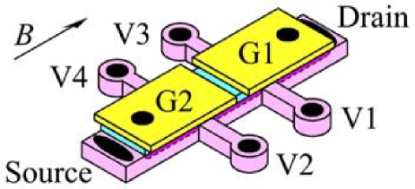
Our experimental scheme enables one to pass a large DC current, , of about 1 A through the source-drain channel, while measuring the dynamic resistance at 12.7 Hz frequency by means of a standard lock-in technique with an AC current of 10–50 nA. Sample temperature was maintained at 0.3 K.
In the first series of measurements, we fix different gate voltages applied to the different areas of the sample across the slot: in area 1, , which corresponds to , and in area 2, , which corresponds to . Then we measure the dynamic resistance of the sample as a function of DC current at zero magnetic field and in parallel fields and 14 Tesla (Fig. 2).
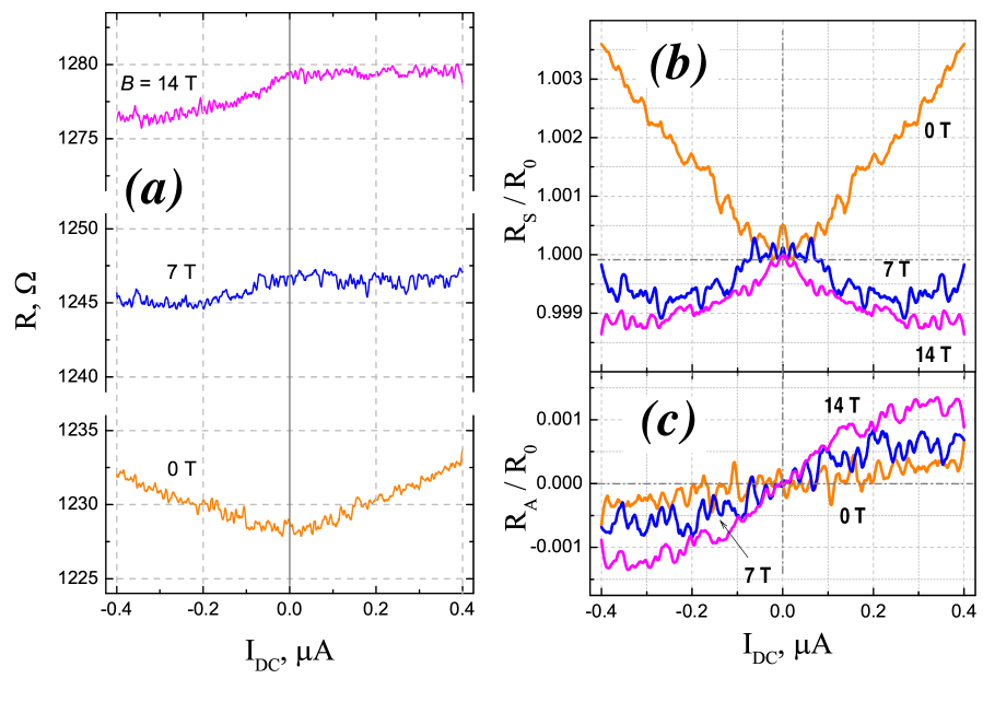
One can see the following features:
(i) At zero , a positive magnetoresistanceShashkin1 ; Simonian ; Tsui ; Shashkin ; Okamoto5 ; Vitkalov ; Lai ; Okamoto8 ; Shlimak12 (PMR) is observed: resistance increases with magnetic field.
(ii) At , resistivity slightly increases with the DC current, and is almost symmetric with respect to the direction of .
(iii) At and 14 T, the dependencies are clearly asymmetric. This asymmetry, which increases with , does not depend on the direction of the magnetic field: the shape of the curves is identical for T and T. This excludes Hall voltage (which may arise due to a slight misalignment of the sample) as a possible origin of the asymmetry.
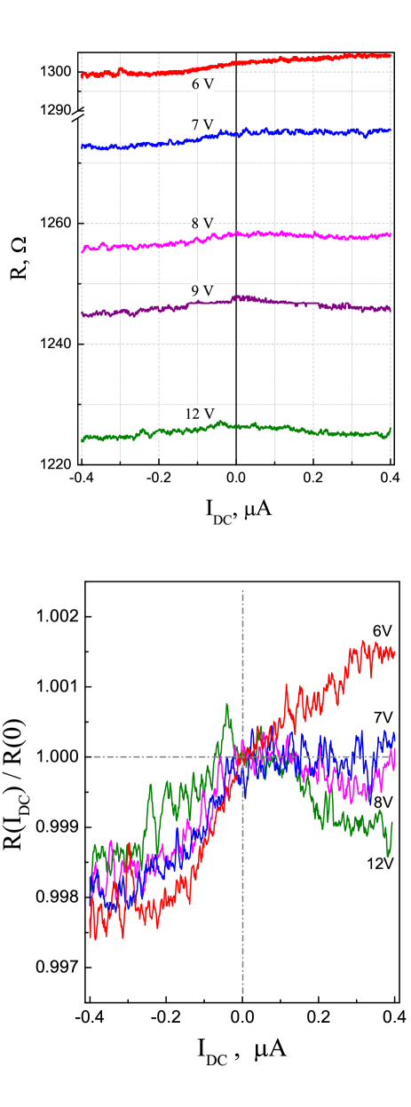
In the second series of measurements, dependencies were obtained at T for the case when one gate voltage was maintained at a constant value, , while the other varied from to ( Fig. 3). One can see that asymmetry increases with the increase of the difference between and .
III Experimental Results and Basic Interpretation – an Overview
Positive magnetoresistance (PMR) effect in parallel magnetic fields in Si-based two-dimensional systems has been observed earlierShashkin1 ; Simonian ; Tsui ; Shashkin ; Okamoto5 ; Vitkalov ; Lai ; Okamoto8 ; Shlimak12 . It was shown in Refs. Shashkin, ; Okamoto5, that the metallic-like conductivity of Si MOSFET first decreases with increase of in-plane magnetic field and then saturates to a new constant value when electrons become fully polarised. This effect is variously attributed to the reduction of screening of charge impurities in a Fermi liquid caused by the loss of spin degeneracyDolgopolov , or to a combined effect of spin polarisation, interaction, and multiple impurity-scatteringZala . The reader is referred to Ref. Kuntsevich, for further discussion. What is important for us presently is that the PMR effect is of spin origin, i. e., the conductivity depends on spin polarisation (or equivalently, on magnetisation), which in turn is affected by the applied magnetic field.
In the present paper, we are interested in the asymmetry of the measured resistance with respect to the sign of . Figs. 2 (b) and (c) show the result of decomposition of into symmetric and antisymmetric parts: , and . For convenience, we show normalised values, . The profile of at is almost symmetric. This symmetric increase is presumably due to the conductivity being strongly affected by the Joule heating (of the electron system), proportional to . In our case, both electron concentrations and correspond to the metallic side of the metal-insulator transition in 2D electron systems, when , so increasing the temperature must lead to a resistance increase, explaining the experimental observation. The small asymmetry observed at (about 2.5 of the net resistance at maximal current) can be explained by an additional voltage bias induced by the DC current: . In MOSFETs, is added to the gate voltage with an appropriate sign (cf. “pinch-off” effect Cobbold ). For our sample geometry, at reaches 1 mV which is, indeed, about 10-4 of the . This leads to a small increase or decrease (depending on the sign of ) of the electron density and corresponding asymmetric contribution to the sample resistance.
It follows from Fig. 2, that in strong parallel magnetic fields ( and 14 T), the Joule heating due do the DC current does not influence the resistance significantly. This is in agreement with observation reported in Ref. Tsui, that in strong parallel fields and conductivity of Si-MOSFET is temperature-independent. As a result, the symmetric part of resistance almost disappears. On the other hand, the asymmetric part, , is enhanced and can no longer be explained by the influence of . Indeed, the latter effect is too weak and the associated term in should be linear in and (almost) independent of the magnetic field.
As already mentioned in the Introduction, we suggest that the observed resistance asymmetry of a slot-gate Si-MOSFET in a parallel magnetic field should be understood in terms of the current-induced electron spin accumulation/depletion near the slot. Indeed, at the magnetisation density is uniform and takes value
| (1) |
(in units of Bohr magneton per unit area). Here, is the gyromagnetic ratio, () is the spin-up (spin-down) electron density, and
| (2) |
is the electron density of states per spin projection, taking into account the presence of equivalent valleys (for a Si-MOSFET, ); is the effective mass.
Different electron concentrations across the slot imply different degrees of spin polarisation in the presence of a magnetic field. Within the Drude approach, one obtains a simple relationship between electric () and spin () current densities away from the slot, where the state of the system remains uniform:
| (3) |
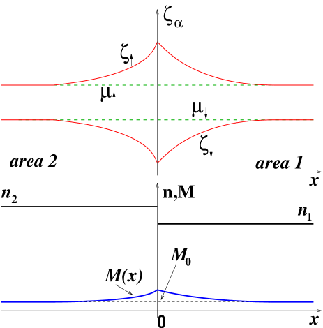
Here is the local in-plane electric field, is the momentum relaxation time, and is electron charge. Consider the case of , corresponding to the flow of (appropriately spin-polarised) electrons from area 1 with high degree of spin polarisation to area 2, where relative spin polarisation is smaller (Fig. 4).

Since (where is the width of the sample) is constant, it follows from Eq.(3) that the flow of the spin density (flowing from right to left in Fig. 4) is larger in area 1 than in area 2, with the excess spin being deposited in the region around the gap. Hence we observe that such a current causes a local increase of spin polarisation near the slot, resulting in an increase of the overall resistance (due to the PMR effect). Conversely, an electron flow from area 2 to area 1 results in a spin depletion and therefore in a decreased resistance. While relegating a self-contained theoretical discussion to the next section, here we quote an expression obtained in the simplest case when the degree of spin polarisation is small everywhere and the spin current is continuous at the slot. While these assumptions are at best inexact, the result is instructive in terms of initial understanding of the data. We find
| (4) |
where is the momentum relaxation time, which can be roughly estimated from mobility, Ref. Shlimak12, . The accumulated excess spin diffuses away from the slot with the rate controlled by the spin relaxation time (also denoted in the context of resonance measurements). Both and depend on the carrier density, and in Eq. (4) we used shorthand notation, viz., , etc.
The first term in Eq. (4) describes the effect of spin accumulation or depletion on via the PMR phenomenon. The PMR effect is parametrised by the derivatives, , which can be determined from the data of Ref. Shlimak12, using a linear fit in the carrier density. Studies of spin relaxation in Si/Si-Ge quantum wells were reported in Ref. Wilamowski, , confirming that is proportional to , as expected for Dyakonov-Perel’ mechanismDyakonov of spin relaxation. The ratio was measuredWilamowski as . Subsequent measurements yielded for Si/Si-Ge quantum wellsTyryshkin and for a Si-MOSFETShankar (in the latter case, the values of carrier density and mobility differed strongly from those in our measurements). We therefore conclude that the ratio is not known precisely, leaving us with a certain freedom in the choice of the value of this parameter.
In addition to these PMR-related effects, there is also another contribution to the resistivity, due to the spin diffusion per se. Indeed, maintaining a non-equilibrium value of spin density in the region near the slot requires a steady flow of energy to this region, resulting in an overall resistance increase [cf. Eq. (32) below]. The second term in Eq. (4) is the antisymmetric part of this additional resistance. In our range of parameter values, this term is an order of magnitude smaller than the first one.
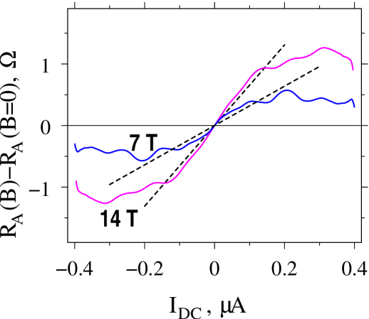
We find that a perfect fit to the experimental at small is obtained if we assume (see Fig. 5), slightly below the reported range.
We also note the pronounced deviation of experimental curves from the linear form of Eq. (4) at larger . This suggests the importance of an additional, non-linear mechanism for dissipating excess spin (of either sign) in a slot-gate MOSFET. Such a mechanism will be introduced in Sec. IV.1. We will then continue with the analysis of our experimental data in Sec. V.
IV Theoretical Model
IV.1 From the Boltzmann Equation to Spin Dynamics
We begin with modelling our system microscopically with the help of a simple Boltzmann equation. Analysis of resultant macroscopic equation for magnetisation is relegated to the next subsection.
We make use of the factWilamowski that the spin relaxation time is much larger than the carrier scattering time . It is this latter time which characterises the momentum relaxation of the system to a “quasi-stationary” state with the distribution function
| (5) |
characterised by the effective chemical potentials . Here, is the energy of the bottom of the band, which depends on the co-ordinate (along the sample) and is determined primarily by the gate voltage. Strictly speaking, it is also affected by the source-drain bias (cf. pinch-off effect in field-effect transistors Cobbold ). The latter effect gives rise to a small correction, , to the measured resistance. This and the larger term due to spin-transport effects (which is of interest to us here) are additive. We will estimate phenomenologically in Sec. V below, while presently assuming that the value of is independent of the source-drain voltage. The “quasi-stationary” values of the chemical potential for the corresponding spin species, , (which also include the Zeeman energy) are related to the local carrier density and magnetisation density (the latter in the units of per unit area) according to
| (6) |
The quantities relax to their true equilibrium values of (here is the chemical potential) with a large characteristic time . Below we shall see that on a smaller time scale (or when there is a current passing through the system), the values of may depend on . As a consequence, magnetisation may deviate from its uniform equilibrium value , given by Eq. (1).
We describe the relaxation of the system to the “intermediate” equilibrium, Eq. (5), via the Drude-type Boltzmann equation,
| (7) |
Here, is the non-equilibrium part of the distribution function, is the momentum relaxation time (assumed to be spin-independent), and the spin-drag time. The terms containing cancel, corresponding to zero current in the absence of the source-drain electric field . The quantities and are the electron density and the net 2DEG momentum density for the corresponding spin species,
| (8) |
The latter is related to the two-dimensional charge and spin current densities via
| (9) |
where spin is again measured in units of Bohr magneton. The Coulomb spin-drag effectDAmico_drag ; Flensberg gives rise to a “drag” force appearing on the l. h. s. of Eq. (7), and to another channel of momentum relaxation corresponding to the second term on the r. h. s..
In the steady state at low , multiplying Eq. (7) by and integrating yields
| (10) |
Using , we next find
| (11) |
Summing the two equations (11) yields an expression
| (12) |
for the electric field . In principle, this should be solved together with the appropriate Poisson equation and with the spin dynamic equations, to determine , , and self-consistently.
We note that our experimental setup is reminiscent of the one previously considered in the literaturePrivman ; Villegas , whereby the doping level in a (three-dimensional) semiconducting sample is varied abruptly as a function of , resulting in the carrier density jump at . Electrical current is passed along the axis, and while there is no external magnetic field, spin current is injected into the semiconductor from a ferromagnetic tip located away from the plane. It was suggestedPrivman ; Villegas ; Csontos that taking into account the non-trivial dependence of the electric field and of the carrier density (as dictated by the Poisson equation) is essential for correctly describing the system. Here, we wish to argue that the latter complication does not arise in the present case.
When supplemented with the Poisson equation, Eq. (12) leads to a drift-diffusion equation for the electric field . Our current densities are well within the diffusive regime of this equation. Furthermore, we find that in our case, the associated diffusion length is of the order of a few nm, which is much smaller than any relevant length scale. The ”smearing” of is therefore insignificant. We conclude that in the range of parameter values of interest to us one can neglect the feedback effect of on and and omit the Poisson equation altogether. This amounts to assuming
| (13) |
where and are the 2DEG densities as set by selecting the appropriate gate voltages at and . The width of the slot, 90 nm, is much larger than the Fermi wavelength for our values of , hence the changes in and affect the quantum-mechanical carrier motion only adiabatically. Accordingly, one can assume that the carriers pass across the slot region in a ballistic fashion [as opposed to tunnelling; treating the slot as a tunnelling barrier with a finite spin-dependent conductance yields only a quantitative change in the resultant dependence]. Note also that we do not attempt to model the profile of [and ] within the slot, since the slot width is smaller than the characteristic length scale of the spin dynamics (spin diffusion length). The term in Eq. (12) is compensated over short distance by the density variation, , (as described by the Poisson equation and independently of the source-drain bias) and both terms can be dropped. Eq. (12) then merely yields the value of as a function of current density (a constant playing the role of experimental control parameter) and magnetisation . The latter is determined by the spin dynamics, to which we will turn now.
Subtracting the two equations (11) from each other, we find the following expression for the spin current [in units of :
| (14) |
where
| (15) |
Thus, the effect of the Coulomb spin drag on spin dynamics in our case consists in a mere relaxation time renormalisationFlensberg . The precise value of is not known, but is expectedDAmico_drag to be small at low temperature . Therefore when comparing our theoretical results with the experimental data in Sec. V, we will assume . We also note that the last (diffusive) term in Eq. (14) vanishes in a uniform system () or for the case of complete spin polarisation ().
The continuity equation for magnetisation reads
| (16) |
The spin relaxation time, , is due primarily to the Dyakonov-Perel’ mechanismWilamowski ; Dyakonov . It does depend on , but an increase of temperature (which might occur due to Joule heating) does not affect the value of as long as is small compared to the Fermi energyDyakonov . Likewise, the effect of the electrical current on is negligible if the carrier drift velocity is much smaller than the Fermi velocity. Since the latter two conditions are certainly met in our experiments, we can assume that is determined solely by the carrier density .
In order to proceed with solving Eqs. (14) and (16) in the steady-state (see the next subsection), we need to specify the boundary condition for at the point of density jump, . This can be done by replacing the step in Eq. (13) with a smooth density change from to , occurring in the range , and taking the limit . Eq. (14) is valid for smooth and , and must yield a finite value of spin current . Since it includes , but not [which is divergent at and might have compensated for a jump in in this limit], we conclude that magnetisation must be continuous at (cf. Ref. Pershin, ). One can arrive at the same conclusion by noticing that the two chemical potentials must be continuous at the slot. This would be modified when a finite tunnelling conductance through the slot is assumed, resulting in a current-dependent magnetisation step. As noted above, this modification does not affect our results in a qualitative way, hence infinite slot conductance will be assumed forthwith.
We further emphasise that must be continuous at only as long as the spin-polarisation on both sides of the slot remains incomplete, . This is due to the fact that the second term in Eq. (14) vanishes at . Whenever full polarisation is attained on either side of the slot, the magnetisation can suffer a jump at , and the limiting value of on the opposite side is determined by the boundary condition for spin current at the slot (see below). Presently, however, we shall be interested in the case of incomplete polarisation only.
Our data imply that in addition to the Dyakonov-Perel’ mechanism [which is linear, see Eq. (16)], another route of spin dissipation is involved, accounting for the saturation of the antisymmetric resistance at larger , as seen in Figs. 2 and 5. This additional mechanism must be non-linear. While in principle it could arise from a sublinear correction to the transport and spin relaxation equations considered above, this would require much higher values of . We conclude that a strongly non-linear “leakage” of spin near the slot into a “spin reservoir” must be present. Assuming that the current does not flow through this reservoir, the chemical potentials for spin-up and spin-down electrons within the reservoir would retain their equilibrium values, . There are several possible realisations of this mechanism, and in the remaining part of this subsection we will describe two examples.
We notice that in the vicinity of the slot, due to the absence of the gate potential, the region of -type Si approaches the surface of the sample, thus potentially enabling electron tunnelling between the 2DEG and the bulk. In the absence of , carriers in the bulk are at equilibrium with the 2DEG, which means that the chemical potentials for spin-up and down electrons have the same respective values, . At , these bulk values of chemical potentials do not change, whereas those of 2DEG acquire the respective quasi-stationary values, . Since the carrier density in 2DEG does not change, one finds . For the tunnelling current density of electrons with spin from the 2DEG into the bulk we write
| (17) |
where the conductance
| (18) |
is assumed to have a spin-independent value in the Ohmic limit. The corresponding tunnelling processes are shown schematically in Fig. 7.
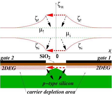
In writing Eqs. (17–18), we make use of the continuity of at the slot, . We denote the corresponding limiting value , as the width of the slot is negligible from the viewpoint of macroscopic equations analysed below. We see that and cancel each other, yet there arises a spin current from the 2DEG into the bulk, with the density
| (19) |
[cf. Eq. (6)]. Thus, the boundary condition for spin current at the slot takes form
| (20) |
where the limiting values of the 2DEG spin current density to the right and to the left of the slot are given by Eq. (14).
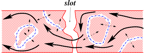
We note that the physics associated with Eqs. (17–19) is not restricted to the specific case of tunnelling into the p-type Si, as described above. Another alternative possibility is related to the fact that the current flow within 2DEG (and especially near the slot) is not necessarily uniform; instead, there might exist sizable regions of 2DEG which do not participate in conduction; these “puddles” would be separated from the “stream”, where the current is flowing, by relatively low tunnelling barriers (see Fig. 8). Due to the absence of current, the respective chemical potentials for the two spin species in the “puddles” retain their unperturbed values, . Hence the “puddles” would play exactly the same role of “spin reservoir” as the p-type Si in the previous scenario. What is essential for us here is that there is a “leakage” of spin current from the source-drain current flow into the reservoir, and that this leakage depends on in a strongly non-linear fashion [cf. Eqs. (18–19)]. The reservoir must be sufficiently large to allow for efficient relaxation of the incoming excess spin.
IV.2 Spin Drift-Diffusion Phenomena, and the Effect on the Sample Resistance
Our first objective here is to find the steady-state profile of magnetisation as a function of the co-ordinate for given values of current and carrier densities . Combining Eqs. (14) and (16) yields the spin drift-diffusion equation,
| (21) |
where
| (22) |
We note that spin drift-diffusion equations were derived earlier by Yu and Flatté for non-degenerate semiconductorsFlatte and by D’Amico for the degenerate caseDAmico_drift ; an interface problem similar to the present one was considered in Ref. Pershin, . In all these cases, the linearisation in was performed, resulting in a linear drift-diffusion equation. On the other hand, the first term of our Eq. (21) is explicitly non-linear. In addition to enforcing a physical constraint, , this non-linearity affects the subleading (in ) terms even for small , which will be important for us here.
At , Eq. (21) is solved by ; other solutions may exist, but these appear irrelevant for the case at hand. As mentioned above, within the present macroscopic description the carrier density [see Eq. (13)], as well as and which depend on , suffer a jump at . In the following, the subscript 1 (2) refers to the quantities characterising the () part of the sample.
We are interested in the diffusive regime of small current densities, for , where
| (23) |
We estimate that for our system, would correspond to a net current which is an order of magnitude larger than our operational valuesjcr .
In the diffusive regime, is small everywhere, and Eq. (21) is easily solved by iterations. Keeping terms of up to second order in , one finds the appropriate solution, decaying exponentially at large ,
| (24) |
where
| (25) |
and
| (26) |
Expressions for are found from the boundary conditions for spin current and magnetisation, as discussed in the previous subsection. To leading order in , we find where the quantity is the solution of
| (27) |
To the required accuracy, we can substitute in Eq. (26). The subleading terms in are given by
| (28) |
Next, we must use Eq. (12) to express the potential difference between the voltage contacts (located at and with ) as
| (29) |
Here, the first term on the r. h. s. corresponds to the Ohm’s law, and in writing it we take into account the fact that the well-known positive magnetoresistance of the 2DEG in a parallel magnetic field B is of spin origin. In other words, depends on via the field dependence of magnetisation , viz., , or . The last term in Eq. (29) originates from the third term in Eq. (12); essentially, this is the additional voltage required to maintain the (non-equilibrium) non-uniform profile of chemical potentials which results in a non-zero [see Eq. (6)].
Dynamic resistance can be found as a derivative of the voltage, Eq. (29), with respect to the net dc-current (where is the width of the sample). We first consider the case of very small current densities, , where
| (30) |
We will have to assume that the quantity [parametrising the non-linearity of tunnelling into the p-type Si, see Eq.(18)] is large, so that this condition is more restrictive than , cf. Eq. (23). Nevertheless, with one can neglect the terms on the r. h. s. of Eqs. (27) and (28), enabling analytical calculation. The dependence of on in this regime is shown schematically in Fig. 9.

Substituting Eq. (24) into (29) and expanding to quadratic terms in the net dc-current , we obtain
| (31) |
where the differential resistance at zero current is
| (32) |
We see that the resistance of two 2DEG areas connected in series is increased due to spin effects, as implied by the presence of the second term. It originates from the third (spin-diffusion) term in Eq. (12), and corresponds to a linear increase of in the diffusive regime (cf. Fig. 9). This non-equilibrium distribution of is maintained by the current flow, which increases the net resistance. In addition, a deviation from the Ohm’s law is obtained, viz., , where
| (33) |
Here, the first term is due to the positive magnetoresistance of the 2DEG (caused by the magnetisation change, , as explained above); the second term is the sublinear contribution of the third term in Eq. (12). In the appropriate limit of and , Eq. (12) yields Eq. (4). For our range of parameter values the first term (which is roughly linear in and hence in ) dominates. This agrees with the experimental at small , as shown in Fig. 2.
We see that the resistance indeed acquires an asymmetric contribution, as seen in Fig. 2. When the net current is small, this contribution is linear in , as per Eq. (33). When becomes comparable to [cf. Eq. (30)], the increase of with slows down and becomes sublinear. This is the origin of saturation in the asymmetric contribution to resistance as seen in the experimental data, Fig. 2. The value of the resistance in this region can be calculated as
| (34) |
where is given by Eq. (29), and its evaluation involves numerically solving Eq. (27) for . Typical profiles of the resultant will be shown in the next section, where these will be compared against the experimental results.
The sublinear behaviour of is due to the non-linear tunnelling to the ”spin reservoir”, Eq. (17–18), which results in a slower growth of the ”effective spin injection” rate with current at larger . One can readily see this analytically in the limiting case of , when the last term in the denominator of Eq. (27) dominates, leading to . In this regime, we find that to leading order, the antisymmetric part of the resistivity, , is proportional to .
V Comparison with the Experimental Data
Here, we attempt a detailed comparison of our experimental data (Sec. III) with the theory developed in Sec. IV. Our focus will be on the antisymmetric part of both theoretical and experimental results. This is because the symmetric part can be affected by additional physical mechanisms, which are unrelated to spin transport and are therefore of no interest to us here. These include the non-linearity in the slot transmission coefficient, and the Joule heating (although, as mentioned above, the effect of heating on resistivity is strongly suppressed when a magnetic field is applied). The antisymmetric part, on the contrary, is due mostly to the spin transport processes as discussed theoretically in Sec. IV, with a smaller antisymmetric contribution due to the effect of the source-drain potential on the 2DEG carrier density (pinch-off).
The latter contribution, present also at , can be evaluated based on the electrical connexion scheme, shown in Fig. 10. At , the carrier densities in the 2DEG are determined by the respective gate voltages, yielding the values of resistivity in the two parts of the sample . At , the resultant electrical potential within the 2DEG layer is added to the gate voltage, and the resistivity acquires a weak dependence on the coordinate , viz., . The overall resistance change between the voltage contacts is linear in ,
| (35) | |||||
and must be added to Eqs. (33–34) when comparing the latter with the experimental data. We note that in the case Eq. (35) accounts for the entire antisymmetric part of the resistance, and indeed a rather accurate fit to the data in Fig. 2 c is obtained.

In Fig. 11 we show the antisymmetric part of measured resistivity for different values of the gate voltage , as plotted in Fig. 3. When attempting to fit these curves theoretically by means of Eqs. (33–34) (dashed lines in Fig. 11), we find that there is a considerable freedom in the choice of the suitable parameter values. Indeed, there is no independent data on the values of the tunnelling parameters and [see Eqs. (17–18)], nor on their dependence on the carrier density . While the value of determines the saturation current density [see Eq. (30)], and therefore the bending of the theoretical curve for , the effect of increasing is rather similar to that of decreasing , hence the values of the latter two parameters are not uniquely determined by the profile of an experimental curve. In the fit shown in Fig. 11 we assumed that the ratio does not depend on the carrier density and equals . The latter choice appears not unreasonable, as it is close to the values reported earlier for Si/Si-Ge quantum wellsWilamowski ; Tyryshkin and for Si-MOSFETsShankar . It differs from the value we used in fitting Fig. 5 above () because presently we include an additional mechanism (tunnelling to a “spin reservoir”, with ). Note that this adjustment of the value of is not an order of magnitude change: the value we use here remains within the experimental range (see discussion in Sect. III).
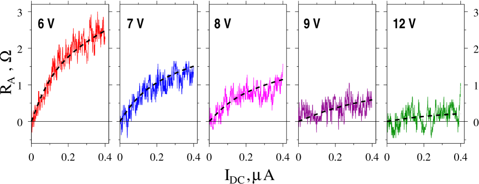
The dependencies of the tunnelling parameters used in Fig. 11 on the gate voltage are shown in Fig. 12. As expected, both and increase with increasing , as the barrier height becomes lower relative to the Fermi energy. Indeed, the entire potential energy landscape (including the tunnelling barriers) is pushed down in energy by increasing gate voltage.

Our assumption that the ratio is independent of was experimentally verifiedWilamowski for the case of the Si/Si-Ge quantum wells, where it is indeed an expected property of Dyakonov-Perel’ spin relaxation mechanism. The case of Si-MOSFETs might be different, but the experimental data on the dependence of on and/or in a Si-MOSFET are lacking. As explained above, in fitting the experimental data in Fig. 11 we could have used different values of for each ; still, perfect fits would have been obtained by appropriately choosing in each case.
We conclude that our theory appears capable of a perfect description of the measured antisymmetric part of the resistance. A more definitive verification of our theoretical picture (and perhaps identification of the underlying microscopic mechanisms) should be possible once the experimental values of the relevant system parameters become available.
VI Conclusion
The observed asymmetric behaviour of the resistance, , of the 2DEG in a slot-gate Si-MOSFET in a parallel magnetic field is clearly due to the spin transport properties of this system. We suggested a phenomenological model which features effective spin injection into the slot region; the rate of this spin injection is controlled by the DC current.
Indeed, the area where the carrier density is smaller is characterised by a stronger spin polarisation (cf. Fig 4). Hence an electron flow (electrical current) in this area is accompanied by a transfer of larger spin per unit time (spin current) than in the case of the same electrical current flowing through the area with larger density. It follows that when electrons flow from the area with smaller carrier density into the area with higher density via the slot region, they must leave excess spin in the vicinity of the slot (spin injection). This translates into an increase of local magnetisation in this region (spin accumulation; cf. Fig.9). This increase is, of course, not unlimited but rather moderated by spin relaxation and diffusion processes. Similarly, when the electrons flow in the opposite direction, local magnetisation near the slot decreases (spin depletion).
The resultant deviation of local spin polarisation of the 2DEG from equilibrium affects the sample resistance, the linkage being provided for the most part by the well-known positive magnetoresistance phenomenon. Since this phenomenon is of spin origin, the resistivity depends on the magnetic field via magnetisation. An increase of the local magnetisation thus leads to an increased resistivity in the region near the slot, and hence to an increased overall resistance. Similarly, spin depletion near the slot results in a decrease in resistance. Our theory yields a good quantitative description of the resistance asymmetry for relatively small values of the DC current, where the antisymmetric part of the resistance is linear in . Therefore it appears certain that we have captured the correct physical mechanism, providing an adequate explanation for the resistance asymmetry in general.
At the same time, the dependence of on at stronger currents becomes sublinear (”saturation”). This implies the presence of an additional, non-linear route for dissipating the non-equilibrium magnetisation density near the slot. We suggest that this is due to tunnelling into a ”spin reservoir”, which could be exemplified by the underlying -type silicon, although other options are also possible. With such a non-linear tunnelling added to our model, we are able to fit the experimental curves for throughout the entire range of current values. This raises the problem of identifying the precise nature of the ”spin reservoir” and directly measuring the tunnelling parameters. In addition, systematic measurements of the dependence of spin relaxation rate on carrier density in a conventional Si-MOSFET (without a slot in the gate) still have to be performed, providing another important input parameter for our theory.
From a broader prospective, we describe and interpret an unusual magnetotransport phenomenon, taking place in a 2DEG with abruptly varying carrier density, in the presence of a parallel magnetic field. The specific realisation of this system (slot-gate Si-MOSFET) can be viewed as incidental. The observed resistance asymmetry highlights new and interesting features of low-dimensional spin and charge transport, and may point to additional possibilities for spin manipulation in microtechnology. It is generally recognised that the efficiency of spintronic devices is limited by finite spin lifetime, due to usual spin-relaxation mechanisms. The observed saturation of resistance asymmetry at stronger current suggests that there are other, significantly non-linear, effects which may have to be taken into account.
Acknowledgements.
The authors take pleasure in thanking R. Berkovits, I. V. Gornyi, B. D. Laikhtman, and L. D. Shvartsman for discussions, and A. Belostotsky and A. Bogush for assistance. This work was supported by the Erick and Sheila Samson Chair of Semiconductor Technology and by the Israeli Absorption Ministry.References
- (1) I. Shlimak, V. Ginodman, A. Butenko, K.-J. Friedland, and S. V. Kravchenko, Europhys. Lett. 82, 47001 (2008).
- (2) A. A. Shashkin, S. V. Kravchenko, V. T. Dolgopolov, and T. M. Klapwijk, Phys. Rev. Lett. 87, 086801 (2001).
- (3) D. Simonian, S. V. Kravchenko, M. P. Sarachik, and V. M. Pudalov, Phys. Rev. Lett. 79, 2304 (1997).
- (4) Y. Tsui, S. A. Vitkalov, M. P. Sarachik, and T. M. Klapwijk, Phys. Rev. B71, 113308 (2005).
- (5) For a review, see G. Schmidt, J. Phys. D: Appl. Phys. 38, R107 (2005).
- (6) I. Shlimak, D. I. Golosov, A. Butenko, K.-J. Friedland, S. V. Kravchenko, Ann. Phys. (Berlin) 18, 913 (2009). Note that theoretical discussion there is in fact inapplicable, as it corresponds to the drift regime of [cf. Eq. 23].
- (7) A. A. Shashkin, E. V. Deviatov, V. T. Dolgopolov, A. A. Kapustin, S. Anissimova, A. Venkatesan, S. V. Kravchenko, and T. M. Klapwijk, Phys. Rev. B73, 115420 (2006).
- (8) T. Okamoto, K. Hosoya, S. Kawaji, and A. Yagi, Phys. Rev. Lett. 82, 3875 (1999).
- (9) S. A. Vitkalov, H. Zheng, K. M. Mertes, M. P. Sarachik, and T. M. Klapwijk, Phys. Rev. Lett. 87, 086401 (2001).
- (10) K. Lai, W. Pan, D. C. Tsui, S. A. Lyon, M. Mühlberger, F. Schäffler, Phys. Rev. B72, 081313 (2005).
- (11) T. Okamoto, M. Ooya, K. Hosoya, and S. Kawaji, Phys. Rev. B69, 041202 (2004).
- (12) I. Shlimak, A. Butenko, D. I. Golosov, K.-J.Friedland, and S. V. Kravchenko, Europhys. Lett. 97, 37002 (2012).
- (13) V. T. Dolgopolov and A. Gold, Pis’ma v ZhETF 71, 42 (2000) [JETP Lett. 71, 27 (2000)].
- (14) G. Zala, B. N. Narozhny, and I. L. Aleiner, Phys. Rev. B65, 020201 (2001).
- (15) A. Yu. Kuntsevich, L. A. Morgun, and V. M. Pudalov, Phys. Rev. B87, 205406 (2013), and references therein.
- (16) R. S. C. Cobbold, Theory and applications of field-effect transistors (Wiley-Interscience, New York, 1970).
- (17) Z. Wilamowski and W. Jantsch, J. Supercond. 16, 249 (2003); W. Jantsch and Z. Wilamowski, in: Spin Physics in Semiconductors, edited by M. I. Dyakonov (Springer, Berlin, 2008), p. 179.
- (18) M. I. Dyakonov and V. I. Perel’, Fiz. Tved. Tela 13, 3581 (1971) [Sov. Phys. Solid State 13, 3023 (2002)]; M. I. Dyakonov and V. Yu. Kachorovskii, Fiz. Tekh. Poluprovodn. 20, 178 (1986) [Sov. Phys. Semicond. 20, 110 (1986)].
- (19) A. M. Tyryshkin, S. A. Lyon, W. Jantsch, and F. Schäffler, Phys. Rev. Lett. 94, 126802 (2005).
- (20) S. Shankar, A. M. Tyryshkin, J. He, and S. A. Lyon, Phys. Rev. B82 195323 (2010).
- (21) I. D’Amico and G. Vignale, Phys. Rev. B62, 4853 (2000); I. D’Amico and C. A. Ullrich, phys. stat. sol. (b) 247, 235 (2010).
- (22) K. Flensberg, T. S. Jensen, and N. A. Mortensen, Phys. Rev. B64, 245308 (2001).
- (23) Y. V. Pershin and V. Privman, Phys. Rev. Lett. 90, 256602 (2003); S. Saikin, Y. V. Pershin, and V. Privman, IEE Proc.: Circuits Devices Syst. 152, 366 (2005).
- (24) L. Villegas-Lelovsky, Appl. Phys. Lett. 89, 012108 (2006); J. Appl. Phys. 101, 053707 (2007).
- (25) D. Csontos and S. E. Ulloa, Physica (Amsterdam) E32, 412 (2006); Phys. Rev. B74, 155207 (2006).
- (26) Y. V. Pershin, Phys. Rev. B68, 233309 (2003).
- (27) Z. G. Yu and M. E. Flatté, Phys. Rev. B66 201202 (2002); B66, 235302 (2002).
- (28) I. D’Amico, Phys. Rev. B69, 165305 (2004).
- (29) Careful examination shows that even if the values of were much lower, the crossover from diffusion to drift regime of Eq. (21), occurring at , would not be sufficient to explain the observed saturation of at large currents (cf. Fig. 5).