The Electronic Structure of CdSe/CdS Core/Shell Seeded Nanorods: Type-I or Quasi-Type-II?
Abstract
The electronic structure of CdSe/CdS core/shell seeded nanorods of experimentally relevant size is studied using a combination of molecular dynamics and semiempirical pseudopotential techniques, with the aim to address the transition from type-I to a quasi-type-II band alignment. The hole is found to be localized in the core region regardless of its size. The overlap of the electron density with the core region depends markedly on the size of the CdSe core: For small cores, we observe little overlap, consistent with type-II behavior. For large cores, significant core-overlap of a number of excitonic states can lead to type-I behavior. When electron-hole interactions are taken into account, the core-overlap is further increased. Our calculations indicate that the observed transition from type-II to type-I is largely due to simple volume effects, and not to band alignment.
Rod-shaped semiconductor nanocrystals Peng et al. (2000) represent a class of nanostructures in which the optical and electronic properties can be tuned by changing the composition, dimensions and shape, offering an ideal model system to study fundamental properties and in particular, the transition between and -dimensional confinement. Recent developments in the fabrication of core/shell seeded nanorods Talapin et al. (2003); Carbone et al. (2007); Talapin et al. (2007); Dorfs et al. (2008); Sitt et al. (2011) have provided an additional knob by which the electrons/holes can either be confined to the core region or the shell. This leads in some cases to a desired intrinsic charge separation Costi et al. (2009) useful for optocatalytic devices.Costi et al. (2008); Amirav and Alivisatos (2010) In other cases, where both electrons and holes are confined to the same region, the nanostructures show remarkable bright and stable fluorescence.Carbone et al. (2007); Talapin et al. (2007) These unique features of semiconductor nanorod heterostructures hold the promise to advance future light harvesting devices.
Perhaps the most studied of the core/shell nanorod structures is that of CdSe core with a CdS shell.Talapin et al. (2003) The hole is known to be localized at the CdSe core due to the large valance band offsets between CdSe and CdS. On the other hand, the conduction band offsets are quite small in the bulk, and thus, the electron can either be localized at the core or at the shell, depending on the size of the core, leading to a possible transition from a type-I to a quasi-type-II band alignment. This has been the focus of numerous experimental and theoretical studies.
Early work using lifetime measurements combined with model calculations hinted to a flat band alignment in which case the electron is confined to the CdS shell and the system is considered to be a quasi-type-II, regardless of the size of the CdSe core.Muller et al. (2004, 2005) More recent experiments based on scanning tunneling spectroscopy (STS) analyzed by a simple effective mass model suggested a conduction band offset of eV, which in principle, would lead to a transition from type-I to quasi-type-II band alignment as the size of the CdSe core decreases.Steiner et al. (2008) This apparent controversy has been addressed using multiexciton spectroscopy (MES) for nanorods with different core sizes, confirming that a transition from type-I (where the electron is localized at the core) to a quasi-type-II (where it is localized at the shell) occurs for a core diameter of nm.Sitt et al. (2009)
Of course, a direct comparison between the STS and MES measurements must be done with care, as the former ignores the interactions between the electron and the localized holes, and thus may lead to a more diffuse electronic state compared to the excitonic state. In fact, the magnitude of this effect has not been addressed so far and will be discussed herein. To add more confusion, this debatable problem has been revisited very recently using time resolved photoluminescence and transient absorption spectroscopies,She et al. (2011) showing that the radiative recombination rate is independent of the CdSe core size, consistent with a quasi-type-II band alignment for all the system sizes studied (i.e., cores above nm). Other recent experimental studies have also revealed the spatial distribution of the wave function Raino et al. (2011); Kunneman et al. (2013) and to long-lived exciton states in CdSe/CdS dot-in-rod structure.Wu et al. (2013)
This controversy has also attracted numerous theoretical and computational studies. Using first-principle calculations, Luo and Wang Luo and Wang (2010) have examined the band alignment of a CdSe/CdS core-shell seeded nanorod (dimensions nm) for a core diameter of nm, finding that the hole is localized inside the CdSe core and the electron in the CdS shell. Since the core size is larger than the expected transition (nm) it contradicts some measurements and calls for a systematic study of the band alignment with the core size.
An alternative approach based on an effective mass model was recently developed by Shabaev et al. Shabaev et al. (2012) for ”giant” CdSe/CdS core-shell nanostructures. They find that the Coulomb potential created by strongly confined holes plays an important role in the electron confinement, a point overlooked by previous studies. Shabaev et al. also examined the effects of core size and CdSe/CdS conduction band offset dependencies on the electronic properties of the nanorod. They found that depending on the band offset, a transition from type-I to quasi-type-II may occur. However, their approach does not provide a quantitative prediction of the actual band offset in CdSe/CdS nanostructures.
In this work, we calculate the electronic structure of CdSe/CdS core/shell nanorods of nm length. We consider two different values of rod diameter, nm and nm, and a number of different core sizes ( nm). The rods are faceted, and the spherical CdSe core was placed at of the length of the rod. The configurations used for the calculations are equilibrium structures relaxed with molecular dynamics runs of ps duration at a temperature of K. For these runs, interactions between atoms were described by a recently developed force-field,Gruenwald et al. (2012) which has been shown to accurately describe CdSe/CdS heterostructures.Gruenwald et al. (2012); Grünwald et al. (2013) The final configuration was quenched to remove structural effects of thermal fluctuations. (See SI for a detailed description of simulation methods.)
The electronic structure calculations of the seeded nanorods were performed within the local version of the semiempirical pseudopotential model,Wang and Zunger (1994); Zunger and Wang (1996); Williamson and Zunger (2000) where the local screened pseudopotentials were fitted to reproduce the experimental bulk band structure, band gaps, effective masses, etc. Furthermore, ligand potentials were used to represent the passivation layer.Rabani et al. (1999) For cadmium and selenium atoms we have used the pseudopotential developed for CdSe Rabani et al. (1999) while for sulfur atoms we have fitted the bulk properties of CdS using the existing pseudopotential for cadmium atoms.sul The pseudopotential for CdS gives a flat band alignment with CdSe in the bulk.Peng et al. (1997) The filter-diagonalization technique Toledo and Rabani (2002) was then employed to filter nearly single particle states near the bands edge. These states were then used to solve the Bethe-Salpeter equation. In order to compare the results to the non-interacting case, we used only one hole state, such that all excitations are associated with electron transitions. We verified that including more hole states does not affect the electron density but adds more excitations associated with hole transitions.
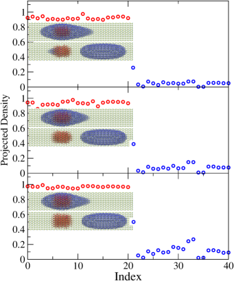
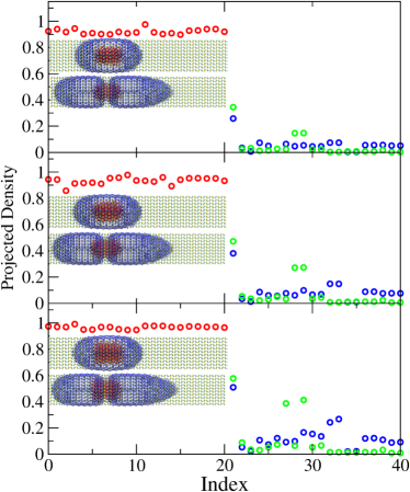
In the left panels of Fig. 1 we plot the integrated projected valance (red circles) and conduction (blue circles) densities onto the core for levels below the valance band maximum and levels above the conduction band minimum. The results are shown for a fixed shell size ( nm) and for core diameters that vary between nm and nm from top to bottom. The inset in each panel shows the hole density of the top of the valance band (red isosurface) and electron density of the two lowest states of the conduction band (blue isosurface), all superimposed on the nanorod frame.
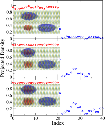
We find that for all valance states calculated, the value of the integrated projected density of the hole is close to unity, implying that the hole is localized in the core with a small probability to leak into the shell region. By contrast, the overlap of the lowest conduction states with the core region depend markedly on core size. For the smallest core considered here ( nm), we find appreciable, but minor, core-overlap of electron density only for the lowest conduction state. All higher states are delocalized in the shell region. With increasing core size, the core-overlap of the lowest state, as well as of a number of higher states, increases markedly, as could be expected from a transition from type-II to type-I band alignment.
The observed increase in core-overlap, however, is not primarily caused by a substantial change in band alignment. In the right panels of Fig. 1, we plot the electron densities of five lowest conduction states, projected onto the nanorod axis. As the core size increases, these densities change only little, as can also be seen in the insets of the left panels of Fig. 1. The biggest contribution to the observed increase in core-overlap thus stems from the increasing core-volume itself. This result indicates that the transition between type-I and type-II behavior is a gradual one. The threshold value of core size at which different behavior is observed will therefore likely depend on the nature of the experimental measurement.
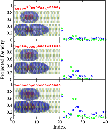
We obtain similar result for a thicker nanorod of same length ( nm) with core sizes ranging from to nm (see Fig. 2). Like in the case of the thinner nanorod, all calculated valance states are highly localized in the core region. Conduction states show an increase in core-overlap with increasing core size. Comparing rods of different diameter, we find that the overlap of the lowest conduction state with the core decreases as the shell diameter increases, consistent with the decrease of the conduction level with increasing nanorod diameter.
This quasi-particle picture is consistent with recent low-temperature STS measurements, suggesting that the electron is somewhat delocalized in the nanorod with a notable amplitude in the core region.Steiner et al. (2008) However, a direct comparison of our predictions with results from STS should be carried out with care: Since the typical broadening in the scanning tip ( meV) is larger than the level spacing in the conduction band ( meV), the transmission is likely to occur through a combination of conduction states rather than a single state. This makes a direct comparison of the degree of localization quite hard. Yet, our results for the lowest conduction state agree well with the experimental observation that tunneling through the lowest conduction state diminishes as one moves the tip away from the region of the core.Steiner et al. (2008)
The single-particle picture discussed in Figs. 1 and 2 might be substantially modified when electron-hole interactions are taken into account.Shabaev et al. (2012) In fact, most experimental studies on the band alignment of CdSe/CdS core/shell nanorods are based on optical measurements in which an exciton is formed and the magnitude of the electron-hole interactions provides a measure of the degree of localization. This is particularly important for situations when the hole is localized at the core and can bind strongly the electron, thereby increasing its overlap with the core.Shabaev et al. (2012) Furthermore, this effect will be strongest for small cores and might therefore be expected to substantially shift the value of core size at which the type-I/type-II transition is observed.
Including the interactions between the electron and the hole is a subtle issue for nanorods, since perturbative techniques that work well for spherical nanocrystals often fail in nanorods as a result of small level spacing.Shabaev et al. (2012); Shabaev and Efros (2004) Here, we resort to the Bethe-Salpeter approach Bethe and Salpeter (1951) within the static screening approximation, where excited states are obtained by diagonalizing the Bethe-Salpeter equation (BSE) with an exciton Hamiltonian give by:Rohlfing and Louie (2000)
where are the single particle states with energies ; label virtual states and occupied states; and are the screened and bare Coulomb potentials, respectively.
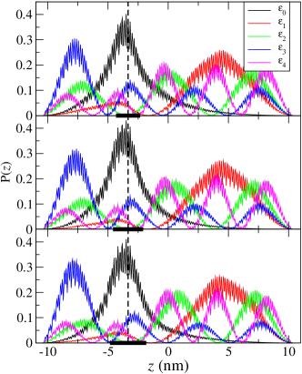
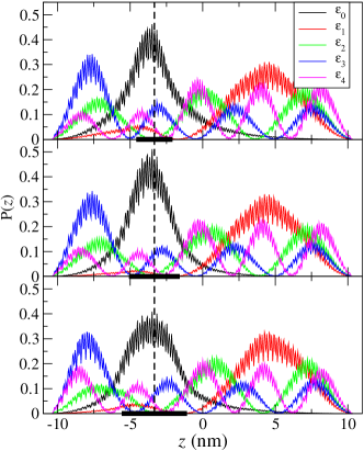
In Fig. 3 we show the results for the projected electron density onto the core obtained from the BSE (green circles) for the nm (left panel) and nm (right panel). For comparison, we also include the integrated projected valance (red circles) and conduction (blue circles) densities onto the core for the noninteracting case shown in Fig. 1 and Fig. 2.
Comparing the maximal value of the electron projected density for the lowest excitonic state, it is clear that including the electron-hole interactions leads to an increase of the overlap of the electron wave function with the core, as one might expect. A pronounced effect is also seen for higher excited states. We find two additional excitonic states that are highly localized near the core region (particularly for the larger seeds). These states may well be associated with recent reports on spatially separated long-lived exciton states in CdSe/CdS nanorods.Wu et al. (2013)
The observed changes in the degree of core-overlap are partly due to marked changes in the shape of electronic densities. The insets for each panel in Fig. 3 show the hole density of the top of the valance band (red isosurface) and electron density of the two lowest states of the conduction band (blue isosurface), all superimposed on the nanorod frame. Similar to the non-interacting cases shown in the insets of Figs. 1 and 2, the isosurface of the lowest state is centered around the core region. The inclusion of electron-hole interactions via the BSE leads to a somewhat tighter electron density around the seed. The density of the second lowest state, however, is profoundly modified from the non-interacting cases, where the electron is mostly confined to the shell region away from the core. In the interacting case we observe a dumbbell-like shape of the isosurface, centered around the core region.
The general trend of increasing core-overlap with core-size remains unchanged by introducing electron-hole interactions. Like in the non-interacting case, the main contribution to this increase is the increasing core-volume itself, rather than a substantial shift in band alignment. Furthermore, we do not observe a strong effect of core-size on the strength of electron-hole interactions, which would lead to increased localization of electrons in the core primarily for small cores.
| 4 | 0 | -6.60 | -4.01 | 2.59 | ||||
| 4 | 2 | -6.38 | -4.10 | 2.28 | 2.14 | 0.46 | 33 | 0.94 |
| 4 | 2.5 | -6.31 | -4.10 | 2.21 | 2.05 | 0.35 | 31 | 1.24 |
| 4 | 3 | -6.25 | -4.10 | 2.15 | 2.00 | 0.23 | 30 | 1.50 |
| 6 | 2.5 | -6.35 | -4.20 | 2.15 | 2.00 | 0.39 | 39 | 0.88 |
| 6 | 3.5 | -6.25 | -4.21 | 2.04 | 1.90 | 0.27 | 37 | 1.28 |
| 6 | 4.5 | -6.15 | -4.21 | 1.94 | 1.82 | 0.23 | 36 | 1.66 |
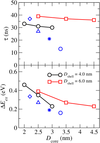
In Table 1 we summarize the relevant energies calculated for the relaxed nanorods configurations. The quasi-particle gaps and the exciton energies for the seeded nanorods are slightly lower ( eV) compared to experimental results.Sitt et al. (2009) This is likely due to the fact that the pseudopotential used in the electronic structure calculations was optimized for a perfect lattice configuration in the neat CdSe and CdS bulk systems, while our calculations were performed for a relaxed hetero-structure. The small overall change in the band gap with the core size (roughly eV going from to nm) is in agreement with the photoluminescence experiments.Sitt et al. (2009) The shift in the position of the hole level is larger than that of the electron since the latter overlaps the shell, which is kept fixed in this process. This is also consistent with STS measurements.Steiner et al. (2008) We find that the conduction band minimum is always below that of a neat CdSe NC (results not shown here) Rabani et al. (1999) for all sizes studied, confirming a very shallow band offset between the core and the shell for the electrons.
Table 1 also shows the energy difference between the first exciton in the core only and core/shell structures () and the radiative lifetime (). These are also plotted in Fig. 4. These quantities depend weakly on the length of the nanorod, but show a pronounced effect with the core diameter and rod diameter. The calculated values are compared with the experimental results for the shift in the absorption peak and the radiative lifetime,Raino et al. (2011) a comparison that can serve to further assess the accuracy of the model. The experimental energy shifts vary from eV to eV when the core size increases from nm to nm in diameter. The theoretical values are slightly larger than the corresponding experimental results. However, our model captures the general trends with core size and the slope of is similar. The comparison is complicated by the fact that experimental values were obtained for nanorods with different (shell) diameters, and no uncertainties are provided in Ref.Raino et al. (2011) for the values of core diameter (or how these values were determined). Assuming a standard deviation of nm, as quoted for the values of shell diameter, our results agree quantitatively with experiments.
Comparing the radiative lifetimes to the experimental values, we find that in both cases decreases with increasing core diameter. The lifetimes are very similar for the smaller cores (on the order of ns), while for the larger cores, we overestimate the lifetimes by more than . The discrepancy may indicate that for larger cores there are defects located at the interface between the two semiconductors which are not included in our model and may affect the slope of the lifetime with core diameter. Alternatively, the experimental lifetimes may include contributions from non-radiative decay, again not included in the theory. The non-radiative decay is expected to be more significant for large cores as the density of phonon changes with the core volume.
Finally, Table 1 also provides the values of the oscillator strength, which increases rapidly with the core size and decreases with the nanorod diameter. The dependence on the core and rod diameters can be explained in terms of the extent of electron localization and the effect of the core and nanorod dimensions on the overlap of the electron wave function with the core, as reported above.
In summary, we have used a combination of molecular dynamics and electronic structure simulation techniques to study the electronic properties of CdSe/CdS core/shell seeded nanorods. For all system sizes considered here, we find strong localization of the hole in the core of the nanorod. The overlap of conduction states with the core region depends on core size: For small cores, minor overlap occurs for the lowest conduction state only; for larger cores, sizable overlap is observed for a number of conduction states. When electron-hole interactions are taken into account, the core-overlap of conduction states increases but the same trend with core size are observed, which is consistent with experimental observations of a transition from type-I to quasi-type-II behavior with decreasing core size. Our results indicate that this transition is not primarily driven by a change in band-alignment, but rather by the change in core volume itself.
Acknowledgement We would like to thank Uri Banin for insightful discussions. HE is grateful to The Center for Nanoscience and Nanotechnology at Tel Aviv University for a post-doctoral fellowship. M.G. was supported by the Austrian Science Fund (FWF) under Grant J 3106-N16. This work was supported by the Israel Science Foundation (grant number 611/11). ER thanks the Marko and Lucie Chaoul Chair.
References
- Peng et al. (2000) Peng, X.; Manna, L.; Yang, W.; Wickham, J.; Scher, E.; Kadavanich, A.; Alivisatos, A. P. Shape control of CdSe nanocrystals. Nature 2000, 404, 59.
- Talapin et al. (2003) Talapin, D.; Koeppe, R.; Gotzinger, S.; Kornowski, A.; Lupton, J.; Rogach, A.; Benson, O.; Feldmann, J.; Weller, H. Highly emissive colloidal CdSe/CdS heterostructures of mixed dimensionality. Nano Lett. 2003, 3, 1677–1681.
- Carbone et al. (2007) Carbone, L. et al. Synthesis and Micrometer-Scale Assembly of Colloidal CdSe/CdS Nanorods Prepared by a Seeded Growth Approach. Nano Lett. 2007, 7, 2942–2950.
- Talapin et al. (2007) Talapin, D. V.; Nelson, J. H.; Shevchenko, E. V.; Aloni, S.; Sadtler, B.; Alivisatos, A. P. Seeded growth of highly luminescent CdSe/CdS nanoheterostructures with rod and tetrapod morphologies. Nano Lett. 2007, 7, 2951–2959.
- Dorfs et al. (2008) Dorfs, D.; Salant, A.; Popov, I.; Banin, U. ZnSe quantum dots within CdS nanorods: A seeded-growth type-II system. Small 2008, 4, 1319–1323.
- Sitt et al. (2011) Sitt, A.; Salant, A.; Menagen, G.; Banin, U. Highly Emissive Nano Rod-in-Rod Heterostructures with Strong Linear Polarization. Nano Lett. 2011, 11, 2054–2060.
- Costi et al. (2009) Costi, R.; Cohen, G.; Salant, A.; Rabani, E.; Banin, U. Electrostatic Force Microscopy Study of Single Au-CdSe Hybrid Nanodumbbells: Evidence for Light-Induced Charge Separation. Nano Lett. 2009, 9, 2031–2039.
- Costi et al. (2008) Costi, R.; Saunders, A. E.; Elmalem, E.; Salant, A.; Banin, U. Visible light-induced charge retention and photocatalysis with hybrid CdSe-Au nanodumbbells. Nano Lett. 2008, 8, 637–641.
- Amirav and Alivisatos (2010) Amirav, L.; Alivisatos, A. P. Photocatalytic Hydrogen Production with Tunable Nanorod Heterostructures. J. Phys. Chem. Lett. 2010, 1, 1051–1054.
- Muller et al. (2004) Muller, J.; Lupton, J.; Rogach, A.; Feldmann, J.; Talapin, D.; Weller, H. Monitoring surface charge movement in single elongated semiconductor nanocrystals. Phys. Rev. Lett. 2004, 93, 167402.
- Muller et al. (2005) Muller, J.; Lupton, J.; Lagoudakis, P.; Schindler, F.; Koeppe, R.; Rogach, A.; Feldmann, J.; Talapin, D.; Weller, H. Wave function engineering in elongated semiconductor nanocrystals with heterogeneous carrier confinement. Nano Lett. 2005, 5, 2044–2049.
- Steiner et al. (2008) Steiner, D.; Dorfs, D.; Banin, U.; Della Sala, F.; Manna, L.; Millo, O. Determination of band offsets in heterostructured colloidal nanorods using scanning tunneling spectroscopy. Nano Lett. 2008, 8, 2954–2958.
- Sitt et al. (2009) Sitt, A.; Della Sala, F.; Menagen, G.; Banin, U. Multiexciton engineering in seeded core/shell nanorods: Transfer from type-I to quasi-type-II regimes. Nano Lett. 2009, 9, 3470–3476.
- She et al. (2011) She, C.; Demortiére, A.; Shevchenko, E. V.; Pelton, M. Using… J. Phys. Chem. Lett. 2011, 2, 1469–1475.
- Raino et al. (2011) Raino, G.; Stöferle, T.; Moreels, I.; Gomes, R.; Kamal, J. S.; Hens, Z.; Mahr, R. F. Probing the Wave Function Delocalization in CdSe/CdS Dot-in-Rod Nanocrystals by Time- and Temperature-Resolved Spectroscopy. ACS Nano 2011, 5, 4031–4036.
- Kunneman et al. (2013) Kunneman, L. T.; Zanella, M.; Manna, L.; Siebbeles, L. D. A.; Schins, J. M. Mobility and Spatial Distribution of Photoexcited Electrons in CdSe/CdS Nanorods. J. Phys. Chem. C 2013, 117, 3146–3151.
- Wu et al. (2013) Wu, K.; Rodriguez-Cordoba, W. E.; Liu, Z.; Zhu, H.; Lian, T. Beyond Band Alignment: Hole Localization Driven Formation of Three Spatially Separated Long-Lived Exciton States in CdSe/CdS Nanorods. ACS NANO 2013, 7, 7173–7185.
- Luo and Wang (2010) Luo, Y.; Wang, L.-W. Electronic Structures of the CdSe/CdS Core-Shell Nanorods. ACS Nano 2010, 4, 91–98.
- Shabaev et al. (2012) Shabaev, A.; Rodina, A. V.; Efros, A. L. Fine structure of the band-edge excitons and trions in CdSe/CdS core/shell nanocrystals. Phys. Rev. B 2012, 86, 205311.
- Gruenwald et al. (2012) Gruenwald, M.; Zayak, A.; Neaton, J. B.; Geissler, P. L.; Rabani, E. Transferable pair potentials for CdS and ZnS crystals. J. Chem. Phys. 2012, 136, 234111.
- Grünwald et al. (2013) Grünwald, M.; Lutker, K.; Alivisatos, A. P.; Rabani, E.; Geissler, P. L. Metastability in Pressure-Induced Structural Transformations of CdSe/ZnS Core/Shell Nanocrystals. Nano Lett. 2013, 13, 1367–1372.
- Wang and Zunger (1994) Wang, L. W.; Zunger, A. Electronic structure pseudopotential calculations of large (1000 atoms) si quantum dots. J. Phys. Chem. 1994, 98, 2158.
- Zunger and Wang (1996) Zunger, A.; Wang, L. W. un. Appl. Surf. Sci. 1996, 350, 636.
- Williamson and Zunger (2000) Williamson, A. J.; Zunger, A. un. Phys. Rev. B 2000, 61, 1978.
- Rabani et al. (1999) Rabani, E.; Hetényi, B.; Berne, B. J.; Brus, L. E. Electronic Properties of CdSe Nanocrystals in the Absence and Presence of a Dielectric Medium. J. Chem. Phys. 1999, 110, 5355–5369.
- (26) We use the following form for the local pseudopotential in momentum space: . The paramters for cadmium are , , and . For selenium: , , , and . For sulfur: , , , and in atomic units.
- Peng et al. (1997) Peng, X.; Schlamp, M. C.; Kadavanich, A. V.; Alivisatos, A. P. Epitaxial Growth of Highly Luminescent CdSe/CdS Core/Shell Nanocrystals with Photostability and Electronic Accessibility. J. Am. Chem. Soc. 1997, 119, 7019–7029.
- Toledo and Rabani (2002) Toledo, S.; Rabani, E. Very Large Electronic Structure Calculations Using an Out-of-Core Filter-Diagonalization Method. J. Comp. Phys. 2002, 180, 256–269.
- Shabaev and Efros (2004) Shabaev, A.; Efros, A. 1D exciton spectroscopy of semiconductor nanorods. Nano lett. 2004, 4, 1821–1825.
- Bethe and Salpeter (1951) Bethe, H.; Salpeter, E. ”A Relativistic Equation for Bound-State Problems. Phys. Rev. 1951, 84, 1232.
- Rohlfing and Louie (2000) Rohlfing, M.; Louie, S. G. un. Phys. Rev. B 2000, 62, 4927.
- Jain et al. (2012) Jain, P. K.; Ghosh, D.; Baer, R.; Rabani, E.; Alivisatos, A. P. Near-Field Manipulation of Spectroscopic Selection Rules on the Nanoscale. Proc. Natl. Acad. Sci. USA 2012, 109, 8016–8019.