A scalable, fast and multichannel arbitrary waveform generator
Abstract
This article reports on the development of a multichannel arbitrary waveform generator (MAWG) that simultaneously generates arbitrary voltage waveforms on 24 independent channels with a dynamic update rate of up to 25 Msps. A real-time execution of a single waveform and/or sequence of multiple waveforms in succession, with a user programmable arbitrary sequence order is provided under the control of a stand-alone sequencer circuit implemented using an FPGA. The device is operated using an internal clock and can be synced to other devices by means of transistor–transistor logic (TTL) pulses. The device can provide up to 24 independent voltages in the range of up to ± 9 V with a dynamic update-rate of up to 25 Msps and a power consumption of less than 35 W. Every channel can be programmed for 16 independent arbitrary waveforms that can be accessed during run time with a minimum switching delay of 160 ns. The device has a low-noise of 250 µVrms and provides a stable long-term operation with a drift rate below 10 µV/min and a maximum deviation less than ± 300 µVpp over a period of two hours.
I Motivation
Ion traps have promising potential in the field of quantum information science (Cirac and Zoller, 1995; Blatt and Wineland, 2008; Johanning, Varon, and Wunderlich, 2009; Blatt and Roos, 2012), and in particular micro-structured Paul traps are well suited for this purpose. They can have multiple zones for trapping, processing and storing of atomic ions (Kielpinski, Monroe, and Wineland, 2002; Schulz et al., 2008; Kaufmann et al., 2012; Wilpers et al., 2012; Kunert et al., 2013). Scaling such traps up for quantum information processing requires a large number of independent high bandwidth, low noise voltage signals.
In this approach, a register of quantum bits (qubits) is stored in the internal states of laser-cooled trapped ions (forming a Wigner crystal), and in some implementations in motional states of their normal modes (Cirac and Zoller, 1995). Wigner crystals of increasing length become difficult to cool and to protect against environmental influences and thus are subject to decoherence. This is detrimental for tasks that rely on the computational power of quantum superpositions and entanglement. Splitting the quantum register into crystals of manageable size and entangling them on demand in a quantum network is regarded as a promising and straight-forward solution. This can be achieved in segmented ion traps where storage, shuttling and processing zones (Wineland et al., 1998; Kielpinski, Monroe, and Wineland, 2002) are realized by a large number of DC electrodes. These type of traps are often regarded as a prerequisite to scalable quantum information processing using trapped ions.
Specific implementations of such a partitioned quantum register require shuttling of ions in order to be able to exchange information between independent crystals and this is ideally done with low heating of the motional state (Wineland et al., 1998). This can be achieved by shuttling of the ions in an adiabatic fashion, at the expense of long shuttling times (Rowe et al., 2002), or in an tailored diabatic way which can be optimized for low heating (Schulz et al., 2008; Walther et al., 2012; Bowler et al., 2012). The latter requires voltages with a fast update rate.
Another building block of this type of quantum information processing is splitting and merging strings of ions, again requiring precise control over a large number of voltages (Eble et al., 2010). Various proposals for processing quantum information exist, among others the network model (Steane, 1998; Sasura and Buzek, 2002), or measurement based quantum computation (Raussendorf, Browne, and Briegel, 2003), relying on highly entangled graph states, which could be generated in ion traps (Wunderlich et al., 2009).
Shuttling and the tailoring of interactions cannot only be done by manipulating the DC voltage, but also the RF voltage used for radial trapping of an ion string (Kumph, Brownnutt, and Blatt, 2011). A general purpose quantum processor would be a field programmable trap array (FPTA). Independent arbitrary time-dependent potentials (e.g., sums of dc and rf voltages) can be applied to each element of the FPTA, allowing for the creation of arbitrary trapping potentials (compared to designs optimized for a fixed lattice (Schmied, Wesenberg, and Leibfried, 2009)) and the investigation of various lattice types and quantum simulations thereof with a single programmable trap (a similar concept is discussed in ref.(Lybarger, 2010)). For certain types of ions and trap sizes the device presented here already fulfills all the necessary requirements. This type of application might require – depending on the selected ion and trap design – higher amplitudes or update rates than supplied by the device described here, and, to reduce heating, narrow band filtering of the RF component.
Similarly, quantum simulators require a high degree of control to simulate the features of other quantum systems (Johanning, Varon, and Wunderlich, 2009; Schneider, Porras, and Schaetz, 2012; Blatt and Roos, 2012). The interaction between trapped ions could be tailored to mimic an entirely different quantum system, for example by shaping the axial trapping potential (Wunderlich and Balzer, 2003; Khromova et al., 2012). This application, too, requires a large number of independent voltages.
Furthermore, in the field of experimental quantum optics, laser fields are often used to manipulate the internal or motional state of atoms, and need to be shaped in time and space. Shaping the temporal profile of laser pulses can be realized using acousto-optic modulators (AOMs), where control signals can be used to generate arbitrary amplitude and frequency patterns of a laser (DeMaria and Stetser, 1965; Jolly and Estraillier, 2004). The spatial profile of a laser beam can be manipulated by a spatial light modulator (SLM), typically implemented as a liquid crystal display (LCD) or digital micro-mirror devices. The SLMs often take digital signals for control using pulse width modulation, but analog implementations exist (Serati et al., 1995) potentially requiring again a large set of independent voltages. In the same fashion the spectral and accordingly temporal profile of large bandwidth lasers and frequency combs can be manipulated (Weiner, 2000). Other applications in the quantum optics community, for example, the generation of control signals to shape magnetic or dipole traps for neutral atoms (Grimm, Weidemüller, and Ovchinnikov, 2000; Folman et al., 2002) and using SLMs for wave front sensing, adaptive imaging, and holography also require a large number of individual voltages.
Commercially available devices do not meet the requirements of precise enough voltages combined with a fast update rate as needed for quantum optics experiments. This article reports on the design, development, and characterization of a scalable, fast and multichannel arbitrary waveform generator (MAWG)(Baig et al., 2012) that meets the requirements of advanced quantum optics experiments.
II Hardware architecture
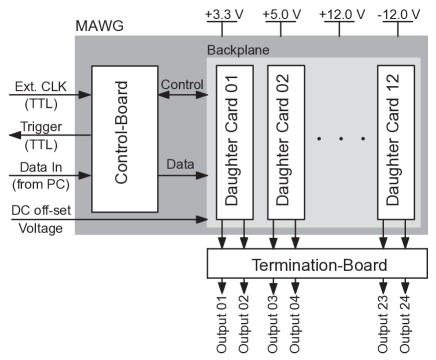
A general architecture of the device is shown in Fig. 1. The MAWG consists of a control-board interfacing with 12 identical daughter-cards via a backplane. The control-board receives the waveform-data as well as control instructions from a control computer via a USB 2.0 interface. A field programmable gate array (FPGA) on the control-board decodes the control instructions and stores the provided waveform-data on the memory of a desired daughter-card or retrieves the pre-stored waveform-data from the memory of the daughter-card according to the control instruction. The backplane provides distribution of signals and voltage supplies to all of the daughter-cards. Each daughter-card has two channels to generate two independent voltages which are individually terminated and low-pass filtered on a remote termination-board resulting in the final voltage signals to be used in the desired application. A dedicated synchronous dual-port static RAM (DP-SRAM) is provided to each of the daughter cards to store waveforms data for every channel individually up to 128 k depth. A complex programmable logic device (CPLD) on every daughter card controls the flow of the data and the clock to both of the channels locally. The general architecture of the MAWG with flow of data signals among main parts of the device is shown in Fig. 1
| Component | Company | Part # |
|---|---|---|
| USB µC | Cypress Semiconductor | CY7C68013A |
| FPGA | Xilinx Inc. | XC3S500E |
| Serial EEPROM | Microchip Technology | 24LC64 |
| CPROM | Xilinx Inc. | XCF04S |
| Crystal | Vishay | XT49M |
| Oscillator | IQD Frequency Products Limited | IQXO-22C |
| CPLD | Lattice Semiconductor | ISPMACH4064V |
| DP-SRAM | Integrated Device Technology | 70V3599 |
| Voltage Reference | Maxim Integrated | MAX6161 |
| DAC | Maxim Integrated | MAX5885 |
| OP-AMP | Analog Devices | AD8021AR |
| Digital Isolator A | Analog Devices | ADUM1100BRZ |
| Digital Isolator B | Analog Devices | ADUM1401CRWZ |
| Octal Bus Transceiver | Texas Instruments | SN74LVT245B |
| DC-DC Converter | Texas Instruments | TPS54610PWP |
The MAWG is optimized to get a good quality signal (in terms of low reflections, drift and noise) for operations up to an update rate of 25 Msps. A user defined internal clock, provided by the FPGA on the control board, or an external transistor–transistor logic (TTL) signal can be used to operate the device in an asynchronous or synchronous mode of operation respectively. In addition, a TTL pulse signal is provided by the MAWG device to trigger the operations of other devices in the experiment. The user-defined voltage waveforms can optionally be shifted by a DC off-set voltage.
The updating of waveforms in the device memory - the write operation - is done sequentially, channel-by-channel with one channel at once, while the actual generation of voltages - the read operation - is executed simultaneously and synchronously for all of the 24 channels. Provision of the dedicated memory for each channel and simultaneous read for all channels correspond to a digital bandwidth of 9.6 Gbps.
A list of the main integrated circuit components (ICs) used for the MAWG device is provided in Table 1. 111All devices and components listed are specified for traceability purpose only and are not mentioned for advertising them, nor do we claim superior performance. All components were chosen to satisfy various assessment criteria, importantly, high dynamic range of speed and amplitude, supportive contribution to low-noise and environmental stable performance, as well as possibly general simplicity and high reliability at the same time.
II.1 The control board
The control-board holds both fixed- and firmware-type circuitry, which are primarily needed to receive user-defined waveform and/or control instructions sent from the control computer, and furthermore to process and to deliver them to the daughter-cards through the backplane in a controlled way.
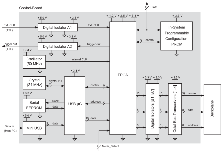
The data is received from the control computer by the USB micro-controller (µC) via the USB interface and delivered to the FPGA in a 2-bytes word format. The FPGA analyses the data and delivers a single-byte-oriented output either directly or using its internal block-RAM to the backplane in case of the instructions or the waveform-data respectively. All outputs of the control-board are galvanic-isolated followed by a signal-current enhancement provided by octal bus transceivers. A configuration programmable read-only memory (CPROM) and a serial electrically erasable programmable read-only memory (EEPROM) are used to auto-configure the FPGA and the USB µC after power-up respectively. The components of the control-board and the data flow among them are detailed in Fig. 2.
All voltage supplies required by the components on the control-board (1.2 V, 2.5 V, 3.3 V and 5.0 V) are down-converted on-board from a single +5.0 V supply using DC-DC converters. A galvanic isolated TTL compatible input and output is provided to synchronize operation of the device with rest of the devices in the experiment. The TTL input can be used either as a trigger for internal clock or to apply a signal as an external clock for the synchronized use of the MAWG.
A 24 MHz crystal is used by the USB µC to generate internally 480 MHz and 48 MHz clocks needed for USB data transmission. Furthermore, a 50 MHz on-board oscillator is used by the FPGA to generate clock signals by means of internal frequency divisions, which are needed for the write and the read operations of the MAWG
II.2 The backplane with the daughter-cards
The backplane holds 12 identical daughter-cards such that each daughter-card shares a common data-, control- and address-bus. The waveform-data received from the control-board is delivered to a daughter-card via the backplane during the write operation of a channel on the daughter card. All bus lines are impedance-matched and resistor-terminated on the backplane. Three supply voltages +3.3 V and ± 12 V (optionally ± 15 V) generated by a dedicated external power supply are distributed to each daughter-card trough the backplane.
All power lines are protected by Zener diodes at the entrance of the backplane.
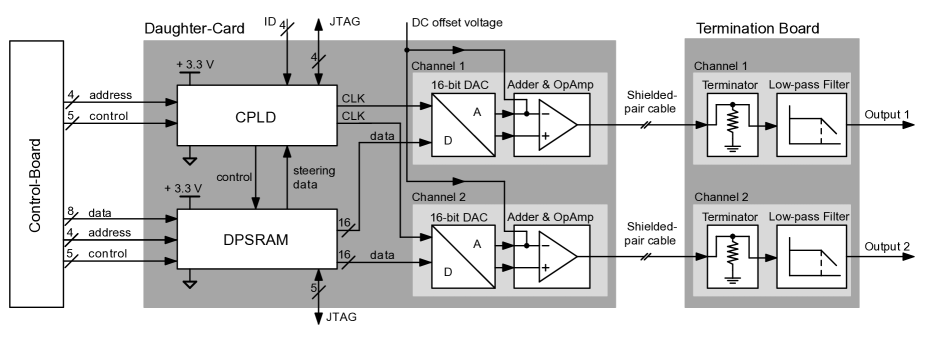
The daughter-card contains the circuitry to generate two independent voltages. The key components used on the daughter-card along with a flow of data and control signals are shown in Fig. LABEL:fig:BlockDia_DaughterCar. The CPLD controls signals received by the card and generates clock pulses for the digital-to-analog converter (DAC) along with the control signals to the DP-SRAM on the same daughter-card. The control signals manage storage of the data to a particular address of the DP-SRAM when a write operation of the MAWG is executed or deliver the stored data from a particular address of the DP-SRAM to the desired DAC when a read operation of the MAWG is performed. The CPLD and the DP-SRAM serve for both channels of the respective daughter-card. Each 16-bit DAC converts respective digital code into a pair of analog signals and delivers it to the operational amplifier (OP-AMP). The output voltages provided by a daughter-card are coupled to a shielded-pair cable with 110 characteristic impedance. The key components of the daughter-card are listed in Table 1.
A channel on the daughter-card can be operated in two modes of operation, stopped-clock and continued-clock. In the stopped-clock mode the DAC of the channel holds last value of the voltage sequence being read from the DP-SRAM without getting further clock signal from the CPLD whereas in the continued-clock mode the DAC gets a continuous clock and refreshes the last value of the voltage sequence being read from the memory with the user-defined clock update rate.
II.3 A channel on the daughter-card
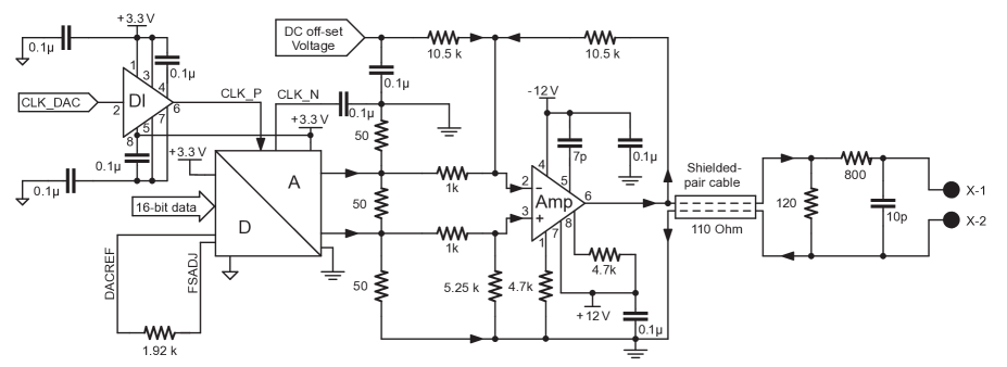
A single channel on a daughter-card consists of a complementary current-type-output 16-bit DAC, followed by a low-noise, high-speed OP-AMP in differential configuration with a gain equal to 10. The DAC converts the user defined voltage code, pre-stored in the DP-SRAM using the write operation, into two corresponding analog current signals with a 16 bit resolution. These current signals are then converted into two voltage drops across 50 resistors, referenced to the analog ground (AGND). The voltage drops are finally subtracted and amplified through the OP-AMP circuit. An optional addition of a DC-offset voltage of up to ± 7 Vpp is also provided which is common to all channels and can be used to shift the reference level of the final output provided that the sum of amplitudes of the actual and offset voltages does not exceed the output amplitude limits of the channel (see Fig. 4).
The DAC is configured to use the full scale output current amplitude (± 2 mA) and to use an internal band-gap reference voltage (1.2 V) provided by the DAC itself. The output of the DAC has a latency of 3.5 clock cycles.
II.4 The memory management on the daughter-card
The DP-SRAM has a total capacity of 128 k words with a word-width of 36 bits. The DP-SRAM is organized by dividing the full word of the memory into two sub-words of 18 bits each, such that each word serves to hold one data code of a channel on the respective daughter-card by using 16 bits, whereas the remaining 2 bits are reserved for optional steering data. The full depth of the DP-SRAM is divided into 16 logical segments of 8 k words each, which in practice reduces the width of address bus to access the memory from 16 to 4 bits and hence results in a reduced digital noise on the daughter-card at the expense of discrete access to the memory only at start-addresses of the 16 segments (Baig et al., 2010).
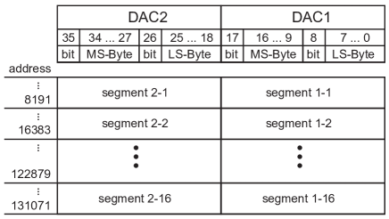
Each segment of the DP-SRAM can be used to store an individual voltage sequence of up to 8 k words. A voltage sequences larger than the size of the segment can be stored on multiple adjacent segments until the end of the memory. Once a memory segment is accessed at the beginning of the write or the read operation, the address-control is passed to the DP-SRAM for further increment of the address, using its internal counter, which can be continued across the segments until the end of the memory. Fig. 5 shows details about the memory address management and the bit-assignment of one 36 bits memory word. The waveforms stored on different segments can be retrieved with a switching latency of 4 clock cycles from one segment to another (e.g., 160 ns for 25 MHz update rate). Writing up the data for full depth of the DP-SRAM of a channel needs around 32 ms.
II.5 Printed circuit boards
The printed circuit boards (PCB) for the control-board and the backplane are designed with 4-layers, while the daughter-cards are designed with 6-layers architecture. Routing of the signals is managed on top and bottom layers, whereas the inner layers are reserved only for power and ground planes with solid and large copper areas, which ensure a good high-speed performance due to provision of shortest return current path for signals, low thermal resistance for heat dissipation, reduced parasitic inductance and up to some extent electromagnetic shielding(Ott, 2001; Ardizzoni, 2005).
The partitioning of the digital and the analog ground- and power-planes keeps them separated to make it sure that rich in noise digital circuitry does not affect the performance of the analog part (Johnson and Graham, 1993; Ott, 2001; Mancini, 2002; Rizvi and Khan, 2005; Hu and See, 2005). On the other hand, the digital and the analog grounds are connected to a single common point with a high impedance resistor to avoid dipole and loop antenna effects due to a difference of potentials and large return path respectively (Ott, 2001; Rizvi and Khan, 2005; Ardizzoni, 2005).
Routing of the digital and analog signals is done with extensive care, such that not even a single digital signal trace is crossing the analog ground or power plane and vice versa. In addition to the careful routing, the clock signal to the DAC is routed through a galvanic isolator (that bridges analog and digital grounds and power planes) to maintain the current-loop separation strictly. In addition to the general mixed-signal design recommendations, the particular PCB design recommendations for the DAC and OP-AMP are also followed to get optimum performance. In particular, the OP-AMP is ensured to have the shortest feedback connection and ground-free area under the signal input traces to avoid ringing and overshoot, as well as to reduce a stray input capacitance(Ardizzoni, 2005).
II.6 Power distribution network
The distribution of electrical power for all IC-components is provided to the daughter-card PCB via dedicated inner planes with large surface and hence low impedance. A hierarchical network of decoupling capacitors is implemented to ensure availability of large amounts of current slowly by bulk capacitors as well as less amounts of current rapidly by small capacitors (Mancini, 2002; Knighten et al., 2005) required by the components on the control-board and the daughter-card PCBs. A low-pass filter with RF inductance and ad two capacitances (of 10 µF and 1 µF) in parallel combination are used at each power supply injection into the daughter-card PCB. A decoupling capacitor of 100 nF is placed as close as possible to each power pin of all ICs which decouples the high frequency noise from the analog ICs and work as a charge reservoir for digital ICs to provide the frequently required charge during switching of digital components to avoid the corruption of logic levelsMancini (2002).
| Implicit Index | Command | Code | Explanation |
|---|---|---|---|
| StartSequencer | 32 : 0 | Start execution of the command sequencer. | |
| SetUpdateRate | 34 : 2 | Set the update frequency equal to 25 MHz (50 MHz divided by 2). | |
| ExtCLK_Disable | 35 : 0 | Enable internal clock for read operation of the MAWG. | |
| 0 | WaitForPulse | 19 : 0 | Wait for external trigger to start the sequencer. |
| 1 | StartSegment | 02 : 7250 | Output 7250 words starting from beginning of the segment 2 of the DP-SRAM. |
| 2 | Pause | 16 : 255 | Pause the execution for 255 clock cycles. |
| 3 | StartSegment | 05 : 10500 | Output 10500 words starting from beginning of the segment 5 of the DP-SRAM. |
| 4 | Repeat | 17 : 0 : 11 | Repeat 11 times the execution of preceding commands starting from index 0. |
| 5 | SendPulse | 18 : 170 | Issue an output pulse for 170 clock cycles for external synchronization. |
| EndSequencer | 41 : 0 | End execution of the command sequencer. |
Towards the superior goal of reducing the noise voltage in the system, we took several layout related practical measures, among them we satisfied the following key recommendations for mixed-signal PCB design (Smith et al., 1999; Kester, 2000; Mancini, 2002; Fan et al., 2002; Archambeault, 2007; Archambeault et al., 2008; Archambeault, 2009): (1) Selecting ceramic decoupling capacitors with small SMD package and low equivalent series inductance. (2) Placing decoupling capacitors as close as possible to the power pins of the ICs (~4 mm). (3) Maximizing power-to-ground inter-plane capacitance by minimizing the distance between the power and ground planes (~0.4 mm). (4) Eliminating unwanted capacitance between digital power- and analog ground-planes (and vice versa) by avoiding their geometrical overlap.
Since low inductance path from decoupling capacitors to ground plane enhances effectiveness of noise bypassing, its implementation was pursued consequently with high priority during the PCB layout. Based on calculations given in (Archambeault, 2009), the above design considerations would result in an expected inductance of about 2 nH per single decoupling capacitor and a power pin of the IC.
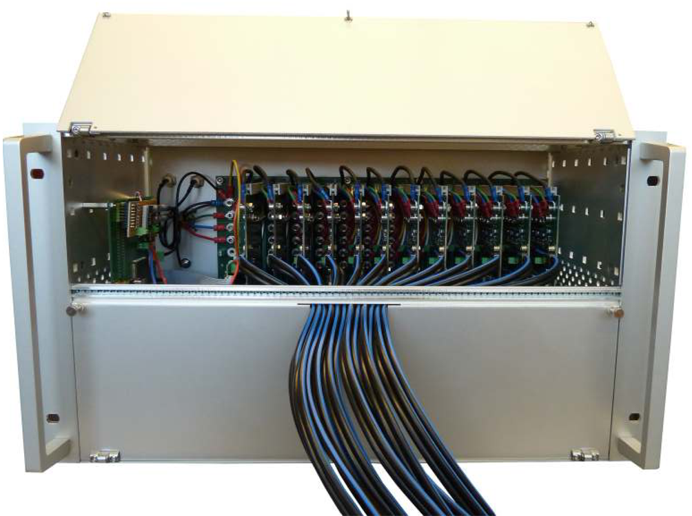
Fig. 6 shows the fully assembled MAWG with the control-board (on left side in the box) and 12 daughter cards mounted on the backplane.
III Software architecture
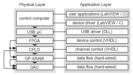
The software needed to run the MAWG was developed in VHDL, C and LabVIEW. The firmware development for the FPGA and the CPLD was done in VHDL and both of the devices are burned with the tested programs using software interfaces provided by the respective vendors. A high-level user-interface to control the MAWG parameters at the run-time is designed in the C as well as in the LabVIEW programming languages. Both applications provide graphical user interface (GUI) for easy access to the MAWG device. Fig. 7 shows a model-based architecture of the developed software along with the flow of information from one physical- and application-layer component to the other one.
The user communicates with the MAWG device by means of sending data-packages for writing into the DP-SRAM and subsequently command-packages for execution in a command sequencer (CS), designed and implemented inside the FPGA. Both communication packages follow a pre-defined data and command bit-formats.
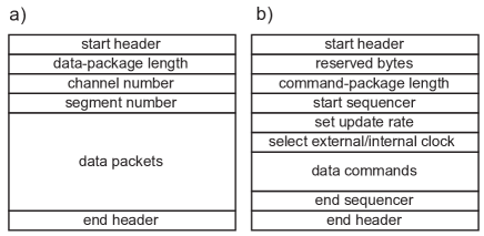
The data-package protocol (Fig. 8a) is used to send the data to be written on the DP-SRAM of a daughter-card. It starts with a start-header followed by information of length of the data-package, the channel number and the segment number to be written. Then comes the data in form of packets of 9 B each and at last the end-header to stop the process of writing the DP-SRAM.
Similarly the command-package protocol (Fig. 8b) consists of instructions to read a pre-stored data from the DP-SRAM and make it available for the DAC. It starts with a start header followed by the length of the command package and the instruction to start the sequencer which encapsulates a list of commands followed by the instruction to end the sequencer and the header. The list of commands consist of configuration commands followed by a combination of five data-handling commands. The configuration commands, SetUpdateRate and ExternalClock, configure the clock update rate for the internal clock or enable/disable the external clock for the read operation of the device respectively. The data-handling commands, StartSegment, Pause, Repeat, WaitForPulse and SendPulse, manipulate the data according to user defined combination of the these commands. All data-handling commands have an implicit index starting with 0. An exemplary command sequencer222Further details about the commands to communicate with device can be provided by the authors on request. is given in Table 2.
IV Performance
IV.1 Generation of arbitrary waveforms
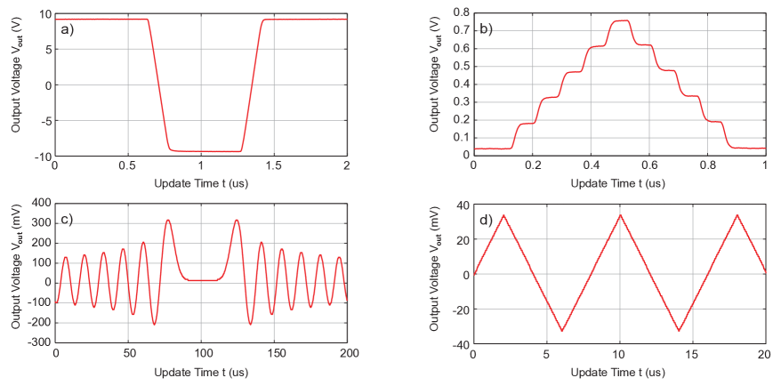
A few exemplary chosen demo-waveform signals generated by the MAWG are displayed in Fig. 9 to demonstrate capability of the MAWG. Fig. 9a presents an abrupt change of voltage from the minimum to the maximum accessible value which shows the amplitude span, the large slew rate, and no visible ringing. Fig. 9b presents a sequence of small fast voltages steps with 80 ns dwell time demonstrating the large bandwidth. Fig. 9c shows the generation of an arbitrary waveforms (here a Bessel function). Fig. 9d presents a triangular waveform showing a good linearity of the output.
IV.2 Output voltage range
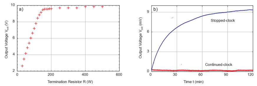
The low-noise OP-AMP (AD8021) has a linear output current limit of 70 mA which determines the maximum output voltage amplitude depending on the value of the termination resistor. A resistor value that needs the amount of current larger than the specified current limit of the OP-AMP will cause saturation of the output voltage. On the other hand, for higher bandwidth output a proper impedance matching between the shielded-pair transmission-line (with characteristic impedance of 110 ) and the termination resistor value on the end of the line is obligatory to minimize the output-signal distortion due to signal reflections. As depicted in Fig. 10a the impedance matching scheme with 120 termination resistor provides a maximum signal amplitude range of ±8.5 V. Though, for low-speed signals of less than 1 Msps, the termination resistor can be increased to 333 , resulting in a less demand for the driving current and consequently providing higher maximum signal amplitude of nearly ±10 V practically without compromising the signal waveform quality. The measured output impedance of the MAWG channel, determined from Fig. 10a at half of the maximum signal amplitude, amounts to 65 .
Another OP-AMP (THS4631D) is tested to provide higher current and hence higher output voltage resulting in maximum output voltages of ±13 V and ±11 V for the low- and high-speed signals respectively and an output impedance of 45 and a thermal dependence of around 200 µV/°C. The OP-AMP is equipped with ± 15 V supply and configured with a gain of 13.
The characterization of the device and results presented are based on the OP-AMP (AD8021) with a termination resistor of 333 .
IV.3 Output voltage precision
The MAWG device has a linear output signal amplitude behaviour over full range of the operation. A discrepancy between the expected and obtained voltages is found to be below ± 4 mV with a standard deviation of 0.81 mV (possibly limited by the measurement device). The discrepancies vary randomly among different channels due to manufacturing imperfections of the components and can be compensated by a software calibration of each channel. The main contribution to the output voltage discrepancy is the offset of the output voltage, which results from an intrinsic OP-AMP input-offset-voltage of typically ± 0.4 mV which results in ± 4 mV after amplification.
IV.4 Output voltage long-term stability
The MAWG device is characterized by dynamic update rates from 25 Msps down to DC-signal generation. Long-term stability of DC output signals is of particular interest for applications in quantum information processing. The static operation of the MAWG channel is determined mainly by the performance of our DAC component, which is specified by the vendor for output signal update rates from 1 Msps to 200 Msps.
In the stopped-clock mode of operation the updating of the DAC is suspended during static output voltages, resulting in an idle state of digital switching. This mode reduces the clock noise on the output signal at the expense of a voltage drift of up to several mV for long term operation with some variations among different channels. On the other hand, in the continued-clock mode of operation, the DAC is updated continuously with a user-defined clock and hence gives an output voltage with higher stability, however with a tradeoff on noise.
An output signal fluctuating around the set voltage with a maximum deviation less than ± 150 µV over a period of 2 h and long term drift with a slope below 10 µV/min is observed when the clock is operated with the minimum specified clock update rate of 1 MHz (Fig. 10b). A combined operation of both modes can be used to get optimum performance. For example, in a particular experiment, the device can be operated in the stopped-clock mode to get the low-noise output during the measurement and then can be switched to the continued-clock mode to get the low-drift output during waiting time between two consecutive measurements.
The overall thermal dependence of the MAWG output voltage is around 70 µV/°C and is measured by a gradual increase of temperature by up to 14 °C starting from the ambient air temperature.
IV.5 Output voltage noise level
The analysis of the MAWG output voltage noise is based on the spectral noise density (SND) of the device measured with the stopped-clock mode of operation. The SND of the MAWG is determined for the full range of its output voltages by taking several voltage spectra for different DC output voltages, whereas a wider spectral range from 1 Hz to 200 MHz was covered by using two different spectrum analysers 333Advantest (R9211B) and Rohde & Schwarz (FSP 30) and later concatenating the resulting spectra for each of the cases (Fig. 11a). The SND spectra are calculated using the relation
where is the noise voltage and RBW is the resolution bandwidth of the spectrum analyser for a particular frequency scan.


The SND spectra of the output of a channel of the MAWG, in the stopped-clock mode of operation, as a function of the frequency are shown in Fig. 11a for a couple of positive and negative output voltages. The spectrum labelled as “333 ” is taken using the bare load-resistor and represents noise contributions from the measurement.
The spectra show discrete contributions mainly from 50 Hz and its harmonics in low frequencies. Some additional noise components are visible at frequencies higher than 1 MHz which are identified as a combined effect of power supply output and pick-up of externally generated radio frequencies. The smooth noise floor of the output voltage has a direct dependence on absolute output voltage up to a frequency of 100 kHz whereas for rest of the observed spectrum this dependence is negligible. A measurement for the MAWG input noise density including power supply output and the 2 m long, multi-pole, interconnect cable is plotted in Fig. 11b which explains the peaks present in the spectra at higher frequencies and hence can be avoided by using a storage power supply and/or implementing a proper low-pass filter at output of the MAWG. In the following analysis, contributions appearing above 100 kHz are therefore neglected.
The increasing noise floor with increasing output voltage (Fig 11c) is caused by an asymmetry between two complementary output currents of the DAC (see section II.3) which are symmetric for 0 V output and become asymmetric otherwise. The asymmetry increases proportionally to the absolute value of the output voltage. A noise cancellation between complementary outputs occurs in the differential OP-AMP, with a maximum noise reduction for the symmetric case and a lower otherwise. On the other hand, the noise floor for each of the output voltage settings decreases strongly with rising frequency. In Fig. 12a the SND is shown as a function of channel output voltage at a couple of frequencies (other than the frequencies corresponding to the 50 Hz harmonics).
The root-mean-square noise of a channel of the MAWG is calculated using the relationship
where is the difference of two consecutive frequencies obtained in the SND measurements.
The output voltage noise as a function of the output voltage () for different frequency spans is plotted in Fig. 12b which shows a linearly increased with increase in output voltage amplitude of the MAWG and reaches a maximum level of nearly 250 µV at ±9 V for the frequency span of 100 kHz. Similarly an increased frequency span results in a corresponding increase in the root mean square noise which remains consistent for all different output voltages.
The signal to noise ratio (SNR) of the MAWG output is calculated for different output voltages using the relationship
The SNR as a function of output voltage is plotted in Fig. 12c for the same frequency spans. The dependence of the SNR on the output voltage is more pronounced for higher bandwidth whereas for constant bandwidth the dependence is strongest on smaller voltages. The bandwidth of 100 kHz has a SNR greater than 90 dB for the output voltages larger than 2 V.
V Conclusions
The MAWG is a general purpose DAC-based system designed to provide multichannel voltage signals characterized by the high dynamic range of both signal amplitude and signal update rate, as well as by a low signal noise and a very good long-term signal stability.
The MAWG is characterized by a large range of signal amplitudes of up to ±9 V, a wide dynamic range of update rates from 25 Msps down to DC signal generation, as well as a low signal-to-noise ratio of +90 dB and long-time stable output signal amplitude within ±0.3 mV. The user-control of the device is provided by means of high-level PC-software applications, as well as device firmware, for storing pre-defined voltage sequences and for generating output signals in real-time. The overall modular concept of the hardware and embedded software allows for a broad flexibility in various operation schemes and particularly in the performance tuning.
Although the detailed specifications of the device are defined in response to technical challenges of experimental quantum information processing, its practical use for other applications in the fields of fundamental and applied research is easily conceivable, especially in those of similar needs for outstanding instrumentation performance.
VI Acknowledgment
We acknowledge funding from the European Community’s Seventh Framework Programme (FP7/2007-2013) under Grant Agreement No. 270843 (iQIT) and No. 249958 (PICC) and European Metrology Research Programme (EMRP) which is jointly funded by the EMRP participating countries within EURAMET and the European Union.
The authors would like to thank Mr. Julius Krieg for his contribution to the design and prototyping of the control-board and Mr. Jürgen Geese for his contribution to the mechanical and electrical assembly of the device.
References
- Cirac and Zoller (1995) J. I. Cirac and P. Zoller, Phys. Rev. Lett. 74, 4091 (1995).
- Blatt and Wineland (2008) R. Blatt and D. Wineland, Nature 453, 1008 (2008).
- Johanning, Varon, and Wunderlich (2009) M. Johanning, A. F. Varon, and C. Wunderlich, J. Phys. B 42, 154009 (2009).
- Blatt and Roos (2012) R. Blatt and C. F. Roos, Nature Phys. 8, 277 (2012).
- Kielpinski, Monroe, and Wineland (2002) D. Kielpinski, C. Monroe, and D. J. Wineland, Nature 417, 709 (2002).
- Schulz et al. (2008) S. A. Schulz, U. Poschinger, F. Ziesel, and F. Schmidt-Kaler, New J. Phys. 10, 045007 (2008).
- Kaufmann et al. (2012) D. Kaufmann, T. Collath, M. T. Baig, P. Kaufmann, E. Asenwar, M. Johanning, and C. Wunderlich, Appl. Phys. B 107, 935 (2012).
- Wilpers et al. (2012) G. Wilpers, P. See, P. Gill, and A. G. Sinclair, Nature Nanotech. 7, 572 (2012).
- Kunert et al. (2013) P. J. Kunert, D. Georgen, L. Bogunia, M. T. Baig, M. A. Baggash, M. Johanning, and C. Wunderlich, Appl. Phys. B, (2013), DOI 10.1007/s00340-013-5722-9.
- Wineland et al. (1998) D. J. Wineland, C. Monroe, W. M. Itano, D. Leibfried, B. E. King, and D. M. Meekhof, J. Res. Natl. Inst. Stand. Technol. 103, 259 (1998).
- Rowe et al. (2002) M. Rowe, A. Ben-Kish, B. Demarco, D. Leibfried, V. Meyer, J. Beall, J. Britton, J. Hughes, W. Itano, B. Jelenkovic, C. Langer, T. Rosenband, and D. Wineland, Quant. Info. Comp. 2, 257 (2002).
- Walther et al. (2012) A. Walther, F. Ziesel, T. Ruster, S. T. Dawkins, K. Ott, M. Hettrich, K. Singer, F. Schmidt-Kaler, and U. Poschinger, Phys. Rev. Lett. 109, 080501 (2012).
- Bowler et al. (2012) R. Bowler, J. Gaebler, Y. Lin, T. R. Tan, D. Hanneke, J. D. Jost, J. P. Home, D. Leibfried, and D. J. Wineland, Phys. Rev. Lett. 109, 080502 (2012).
- Eble et al. (2010) J. F. Eble, S. Ulm, P. Zahariev, F. Schmidt-Kaler, and K. Singer, J. Opt. Soc. Am. B 27, A99 (2010).
- Steane (1998) A. Steane, Rep. Prog. Phys. 61, 117 (1998).
- Sasura and Buzek (2002) M. Sasura and V. Buzek, J. Mod. Opt. 49, 1593 (2002).
- Raussendorf, Browne, and Briegel (2003) R. Raussendorf, D. E. Browne, and H. J. Briegel, Phys. Rev. A 68, 022312 (2003).
- Wunderlich et al. (2009) H. Wunderlich, C. Wunderlich, K. Singer, and F. Schmidt-Kaler, Phys. Rev. A 79, 052324 (2009).
- Kumph, Brownnutt, and Blatt (2011) M. Kumph, M. Brownnutt, and R. Blatt, New J. Phys. 13, 073043 (2011).
- Schmied, Wesenberg, and Leibfried (2009) R. Schmied, J. H. Wesenberg, and D. Leibfried, Phys. Rev. Lett. 102, 233002 (2009).
- Lybarger (2010) J. W. E. Lybarger, Enabling coherent control of trapped ions with economical multi-laser frequency stabilization technology, Ph.D. dissertation, University of California, Los Angeles (2010).
- Schneider, Porras, and Schaetz (2012) C. Schneider, D. Porras, and T. Schaetz, Rep. Prog. Phys. 75, 024401 (2012).
- Wunderlich and Balzer (2003) C. Wunderlich and C. Balzer, Adv. At. Mol. Opt. Phys. 49, 293 (2003).
- Khromova et al. (2012) A. Khromova, C. Piltz, B. Scharfenberger, T. F. Gloger, M. Johanning, A. F. Varón, and C. Wunderlich, Phys. Rev. Lett. 108, 220502 (2012).
- DeMaria and Stetser (1965) A. J. DeMaria and D. A. Stetser, Appl. Phys. Lett. 7, 71 (1965).
- Jolly and Estraillier (2004) A. Jolly and P. Estraillier, Optics & Laser Technology 36, 75 (2004).
- Serati et al. (1995) S. A. Serati, G. D. Sharp, R. A. Serati, D. J. McKnight, and J. E. Stockley, in Proc. SPIE 2490, Optical Pattern Recognition VI (1995) pp. 378–387.
- Weiner (2000) A. M. Weiner, Rev. Sci. Instrum. 71, 1929 (2000).
- Grimm, Weidemüller, and Ovchinnikov (2000) R. Grimm, M. Weidemüller, and Y. B. Ovchinnikov, Adv. At. Mol. Opt. Phys. 42, 95 (2000).
- Folman et al. (2002) R. Folman, P. Krüger, J. Schmiedmayer, J. Denschlag, and C. Henkel, Adv. At. Mol. Opt. Phys. 48, 263 (2002).
- Baig et al. (2012) M. T. Baig, M. Johanning, A. Wiese, M. Ziolkowski, and C. Wunderlich, German Patent No. DE 10 2011 001 399 A1 (20.09.2012), .
- Note (1) All devices and components listed are specified for traceability purpose only and are not mentioned for advertising them, nor do we claim superior performance.
- Baig et al. (2010) M. T. Baig, M. Ziolkowski, M. Johanning, and C. Wunderlich, Verhandl. DPG (VI) 45, 1/A 23.50 (2010).
- Ott (2001) H. W. Ott, Printed Circuit Design 18, 8 (2001).
- Ardizzoni (2005) J. Ardizzoni, Analog Dialogue 39, 3 (2005).
- Johnson and Graham (1993) H. W. Johnson and M. Graham, High-Speed Digital Design : A Handbook of Black Magic (Prentice Hall PTR, Englewood Cliffs, New Jersey, 1993) Chap. 5.
- Mancini (2002) R. Mancini, ed., “Op Amps For Everyone : Design Reference,” (Texas Instruments, 2002) Chap. 17.
- Rizvi and Khan (2005) S. Rizvi and I. Khan, Printed Circuit Des. Manuf. 22, 24 (2005).
- Hu and See (2005) B. Hu and K. Y. See, in Proceedings of 7th Electronic Packaging Technology Conference, 2005. EPTC 2005 (IEEE, 2005), Vol. 1 pp. 34–37.
- Knighten et al. (2005) J. L. Knighten, B. Archambeault, J. Fan, G. Selli, S. Connor, and J. L. Drewniak, IEEE EMC Soc. Newsl. 207, 46 (2005).
- Smith et al. (1999) L. Smith, R. Anderson, D. Forehand, T. Pelc, and T. Roy, IEEE Trans. Adv. Packag. 22, 284 (1999).
- Kester (2000) W. Kester, “Mixed-Signal and DSP Design Techniques,” (Analog Devices, Inc. USA, 2000) Chap. 10.
- Fan et al. (2002) J. Fan, W. Cui, J. Drewniak, T. Van Doren, and J. Knighten, IEEE Trans. Adv. Packag. 25, 154 (2002).
- Archambeault (2007) B. Archambeault, Printed Circuit Des. Manuf. 24, 16-17 (2007).
- Archambeault et al. (2008) B. Archambeault, M. Cocchini, G. Selli, J. Fan, J. Knighten, S. Connor, A. Orlandi, and J. Drewniak, in Electromagnetic Compatibility - EMC Europe, 2008 International Symposium on (2008) pp. 1–6.
- Archambeault (2009) B. Archambeault, IEEE EMC Soc. Newsl. 221, 71 (2009).
- Note (2) Further details about the commands to communicate with the device can be provided by the authors on request.
- Note (3) Advantest (R9211B) and Rohde & Schwarz (FSP 30).