Stone-Wales Defects in Silicene: Formation, Stability and Reactivity of Defect Sites
Abstract
During the synthesis of ultra-thin materials with hexagonal lattice structure Stone-Wales (SW) type of defects are quite likely to be formed and the existence of such topological defects in the graphene-like structures results in dramatical changes of their electronic and mechanical properties. Here we investigate the formation and reactivity of such SW defects in silicene. We report the energy barrier for the formation of SW defects in freestanding (2.4 eV) and Ag(111)-supported (2.8 eV) silicene and found it to be significantly lower than in graphene (9.2 eV). Moreover, the buckled nature of silicene provides a large energy barrier for the healing of the SW defect and therefore defective silicene is stable even at high temperatures. Silicene with SW defects is semiconducting with a direct bandgap of 0.02 eV and this value depends on the concentration of defects. Furthermore, nitrogen substitution in SW defected silicene shows that the defect lattice sites are the least preferable substitution locations for the N atoms. Our findings show the easy formation of SW defects in silicene and also provide a guideline for bandgap engineering in silicene-based materials through such defects.
pacs:
75.70.Ak, 63.22.Np, 61.72.-y, 68.35.DvI Introduction
The electronic, thermal and mechanical properties of graphenenovo ; moriz ; chen ; balan ; lee ; fric are sensitive to lattice imperfections and adatoms. However, the creation of in-plane defects, such as vacancies, adsorption and doping of foreign atoms on the honeycomb structure, opens the possibility for tailoring the electronic and magnetic properties of graphene-based structures.Banhart ; balog ; batzill ; Tapa ; Kras ; gass ; coat It was demonstrated that Stone-Wales (SW) defectsstone can be formed during a rapid quench from high temperature or when graphene is under irradiation.Meyer SW defects have been predicted to open a band gap in the electronic band structure that can be of potential use in the design of transistors.sw1 ; sw2 ; sw3 ; Lusk Moreover presence of such defects modify the chemical reactivity of the graphene lattice.li ; chen2 Very recently, Ijäs et al. have reported that the presence of SW defects in honeycomb lattice results in more reactive domains for chlorine atoms as compared to defect-free graphitic structures.mari
Nowadays, active research on ultra-thin materials has also been directed towards the synthesis and manipulation of monolayer silicon called silicene. In a silicene structure a hexagonal mesh of silicon atoms is buckled and studies show that its electronic properties are similar to those of graphene.takeda ; cahan ; hasan After early theoretical predictions very recent experimental studies have revealed clear evidence of the existence of monolayer honeycomb structures of silicene. In recent works of Vogt et al.vogt and Feng et al.Feng high-quality large-scale silicene films have been synthesized on the Ag (111) surface. Moreover, Fleurence et al. demonstrated the successful growth of epitaxial silicene on a diboride surface.Fleurence Recent theoretical studies have also reported that, prior to graphene, silicene has unique features such as a large spin-orbit gap at the Dirac point,silicene-soc experimentally accessible quantum spin Hall effect,silicene-qshe electrically tunable band gapsilicene-falko and the emergence of valley-polarized metal phase.motohiko Most recently we reported the effect of impurities on the structural, electronic, magnetic properties and lattice dynamics of silicene.silicene-Hasan ; silicene-Jozef
Although the SW type defects are quite likely to be formed in such monolayer systems, the formation of SW-type defects and their effect on the electronic, magnetic and adsorption characteristics of monolayer silicene have remained unexplored. In this paper, we use first-principles calculations within the density functional theory (DFT) formalism to investigate the formation and the electronic properties of SW defects in silicene. We found that formation SW type defects are more likely in silicene than in graphene and the existence of the underlying Ag(111) surface does not significantly affect their formation. Furthermore, once the SW defect is formed in the silicene lattice the doping characteristics are influenced dramatically.
II Computational Methodology
In the present work, we performed first-principles calculations based on the plane-wave basis set with a cut-off energy of 500 eV and the projector-augmented wave (PAW) pseudopotentials implemented in the Vienna Ab-initio Simulation Package (VASP).kresse1 ; kresse2 The exchange-correlation functionals are described by the generalized gradient approximation (GGA) with Perdew-Burke-Ernzerhof (PBE) approach.perdew The partial occupancies for the total energy ground state calculations were calculated with the tetrahedron methodology with Blöchl corrections blochl_1994-tetrahedron .
Periodic boundary conditions were employed for silicene with a vacuum region of 15 Å between neighboring slabs. For supported silicene on a Ag (111) surface the height of the supercell has been set to 29 Å in order to conveniently include 4 layers of the Ag crystal. In order to determine the equilibrium configuration of silicene with defects, we relaxed all the atomic coordinates and the supercell geometry using the conjugate gradient (CG) algorithm with the maximum residual force of less than 0.01 eV/Å. The sampling of the Brillouin zone was done for the supercell with the equivalent of 24241 Monkhorst-Pack monk k-point mesh for a silicene unit cell composed of two Si atoms. In order to minimize the interactions between the neighboring SW defects, for the calculation of geometric and electronic properties, we employed a large supercell derived from a 66 supercell of silicene where the distance between neighboring defects is at least 14.6 Å. The calculations of the formation energetics of a SW defect for supported silicene were performed with a 66 supercell of silicene on top of 88 supercell of Ag (111) surface.
| Å | Å | deg | |||||
|---|---|---|---|---|---|---|---|
| Silicene | 23.21 | 2.28 | 60.0 | 0 | 0.00 | -3.98 | 1.5 |
| SW-Silicene | 23.04 | 2.19-2.28 | 61.5 | 0 | 1.64 | -3.96 | 20 |
III Results and Discussion
III.1 Formation and Stability of Stone-Wales Defects in Silicene
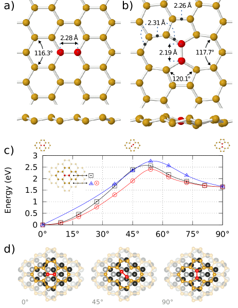
Since the formation of defects is inevitable in crystals, understanding their effect on the mechanical, electronic and structural characteristics plays a key role in nanoscale device applications. The most common defects that have been observed in low-dimensional graphene-like structures are missing atoms, adatom impurities and SW type of disorders. Here we investigate the formation and stability of SW defects in a single layer structure of silicene shown in Fig. 1(a). Compared to the graphitic materials such as graphite, graphene and carbon nanotubes, the inter-atomic distance is larger in silicene. Furthermore, due to the buckled hexagonal lattice structure, easier formation of various defects in silicene can be expected.
As shown in Fig. 1(b) a SW defect can be created by the rotation of a silicon dimer by 90∘ around the center of the Si-Si bond. From the experimental point of view, such a defect can be formed during the growth process or upon application of irradiation. After the formation of the SW defect, four neighboring hexagons of silicene are transformed into a pentagon and a heptagon pair. As can be seen from Fig. 1(b), even after the creation of the SW defect, silicene maintains its buckled two-dimensional structure with only a local out-of-plane displacement of the Si atoms. Conversely, large local bumps in the graphene lattice are formed due to the existence of SW defects. Through 90∘ rotation of a dimer, the Si-Si bond becomes stronger than in defect-free silicene and its length decreases from 2.28 to 2.19 Å. After the shortening of the bond lengths along the direction parallel to the pentagons, the lattice constant decreases from 23.21 to 23.04 Å. Though Si atoms favor buckled configuration in bare silicene the formation of unbuckled Si-dimer in the core of the SW-defect is preferable. Structural properties, energetics and energy band gap of bare and SW-defected silicene are given in Table 1.
The transition states and energetics of the formation steps of the SW defect in free standing silicene as well as for silicene supported on the Ag (111) surface are shown in Fig. 1(c). The intermediate steps are obtained by confining Si atoms at positions interpolated between those of perfect silicene and silicene with a SW defect. The atoms that form two heptagons and two pentagons of the SW defect and the nearest hexagons are allowed to relax. The Si dimer that is gradually rotated is allowed to relax only in the direction perpendicular to the Si layer. It is seen that the formation of such SW defect in a perfect silicene lattice may occur by overcoming the energy barrier of 2.4 eV for free standing silicene and 2.8 eV for the supported silicene layer. The maximum of the energy barrier corresponds to the 54∘ rotation of the bond. In comparison, this barrier in graphitic materials is considerably larger and amounts to 9.2 eV.li However, the energy barrier of 0.76 eV (1.10 eV for supported silicene) between the intermediate configuration and silicene with a SW defect guaranties the stability of such defects even at high temperatures. This shows that the buckled lattice structure and the softer bonding nature of silicene allows an easier formation of SW-defected structure. The formation energy, , of a SW defect in silicene is given by
| (1) |
where is the total energy of silicene with SW defect and is the total energy of perfect silicene. According to this, the formation energy of a SW defect in a 661 supercell is calculated to be 1.64 eV. Additionally, the stability of the structure can also be predicted via its cohesive energy which is defined as the energy required for separating the crystal into isolated free atoms.
The cohesive energy of a crystal structure is given by the formula
| (2) |
where is the total energy of the system, is the number of atoms in the supercell and is the total energy of an isolated silicon atom. The cohesive energies of silicene and SW-defected silicene are calculated to be and eV, respectively. The negative cohesive energies of both structures indicate their stability.
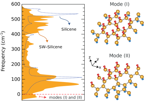
Next we extend our discussion on the stability and formation of SW-type defects in single layer silicene by analyzing the vibrational spectrum. Although total energy calculations show the stability of the SW defects, our phonon calculations reveals that there are two imaginary eigenfrequencies in the SW-defected silicene spectrum (see Fig. 2). For a 44 supercell of silicene these modes are located at and cm-1. Analysis of the lattice dynamics of structure for these two modes shows that the creation of a SW defect results in large ripples around the defected region. As seen from Fig. 2, the modes I and II imply the formation of sinelike and cosinelike lattice distortions with respect to the midpoint of the Si-Si dimer. Therefore the buckled planar structure of SW-defected silicene is a local minimum on the potential energy surface. However, it is worth to note that the stabilization of planar silicene structure by a supporting surface has already been reported by several groups.vogt ; Feng ; Fleurence The existence of sinelike and cosinelike rippling in silicene is in good agreement with the results for SW-defected graphene.sw3 Although our phonon calculations revealed the instability of densely SW-defected silicene, the results also imply the stability provided by the long wavelength ripples. Therefore it is reasonable to assume that the reactivity of defect cores for planar and long-wavelength-rippled silicene do not differ significantly. Additionally, we perform molecular dynamics calculations in order to further examine the thermal stability of SW-defected silicene. At the temperature of 500 K, we choose time steps of 1 and also 2 fs. The SW defect and the surrounding bonds in silicene remain stable and there is no indication of defect-healing throughout the molecular dynamics simulations with duration of 2 ps at 500 K.
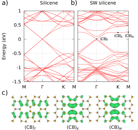
In Figs. 3(a) and (b) the electronic band dispersion of perfect and SW-defected silicene are presented. It is worth to note that for a 66 supercell, the K and K′ symmetry points of the unit cell of silicene are folded onto the point. Therefore, both valence band maximums are transfered to the point of the supercell. Clearly, as seen in Fig. 1(b), after the formation of a SW defect the lattice symmetry of silicene is broken. Since the formation of the SW defect breaks the six-fold symmetry of the silicene lattice, that results in linearly crossing bands and the existence of highly mobile fermions in the vicinity of the Dirac point, a band gap opening occurs at the crossing point.hasan-mesh The band gap opening for SW-defected silicene in a 66 supercell is calculated to be 0.02 eV. It correspond to the system with a defect concentration of 1.91013 cm-2. The actual value of the band gap depends on the concentration of the SW defects. In the case of a 55 supercell with a single SW defect (2.71013 cm-2) the energy band gap increases to 0.1 eV. Here it is also worth to note that the choice of a hexagonal supercell results in band edges that appear at the K symmetry point ( for 33 supercells) and a temporarily ordered defect configuration may result in a different band dispersion. Since there are no dangling bonds introduced into the silicene lattice with the creation of a SW defect, all the atomic orbitals of the Si atoms at the vicinity of the defect are paired and hence there is no defect-originated magnetism.
III.2 N-doped Silicene: Effect of Stone-Wales Defects
Doping materials with foreign atoms is an efficient way to manipulate their electronic, magnetic and chemical properties. For carbon-based materials such as graphite, graphene and nanotubes the doping especially with Group III or V atoms is desirable since they induce or type doping and the density of the charge carriers can be tuned by the concentration of the substituents. It has been demonstrated that synthesis of N doped graphene samples can be achieved by annealing in the presence of pyridine or NH3 molecules and by chemical vapor deposition (CVD) and the observed features of N-doped graphene are quite desirable for device applications. kattel ; Panchokarla ; Zhao ; Wang ; Wei The formation energy of N substitution in graphene is 0.32 eV per N atom.fujimoto_2011 Since N atom in graphene forms three bonds and orbital is filled by two electrons, N-doped graphene shows nonmagnetic behavior.kattel The N doping induces -type doping of graphene and shifts the Fermi level up by 0.6 eV for the case of 2 % N concentration.Panchokarla
The substitutional doping of silicene with a N atom is of a different nature as compared to the doping of graphene. The N-Si bond length in substituted silicene (1.83 Å) is significantly shorter than the Si-Si bond length in pristine silicene (2.28 Å) and the shorter bonds induce a local in plane shrink deformation in the structure as presented in Fig. 4(b). The nitrogen bonds with the neighboring Si atoms are in the plane, which reduces the amount of local buckling. However, perfect silicene’s lattice structure is restored just several bonds away from the substituent atom. The formation energy of N-doping in silicene is defined as
| (3) |
where is the total energy of the N-doped silicene and is the total energy of perfect silicene, is the chemical potential of a single silicon atom (calculated from the total energy of monolayer silicene), and is the chemical potential of a nitrogen atom, defined as one-half of the total energy of the molecule in the gas phase. This choice of chemical potentials is made to account for the stability of N-doped silicene against molecular desorption. The binding energy of N-doped silicene is here defined as:
| (4) |
where is the number of Si atoms in a supercell of pristine silicene and is the total energy of an isolated N atom. The binding energy of a N atom in N-doped silicene is eV. On the other hand, the calculated formation energy is 0.59 eV as a consequence of the large bond-dissociation energy of the molecule.
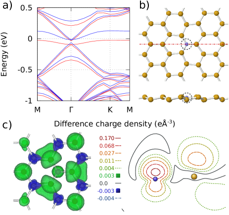
From the electronic band structure of N-doped silicene, displayed in Fig. 4(a), it is seen that the substitutional N atom turns semimetallic silicene into a ferromagnetic metal with total magnetic moment of 1.0 . The magnetic character of N substituted silicene can be seen from the 3D and the contour plot of the difference charge density () in Fig. 4(c). It appears that the N-originated state is delocalized over the nearest Si atoms and therefore N substitution results in long-range spin polarization of the surrounding sp3-like orbitals even in a large 66 supercell. The magnetic behavior of N-doped silicene and delocalization of the N-originated states are consistent with previously-reported results obtained with the use of LDA functionals.silicene-Hasan ; silicene-Jozef
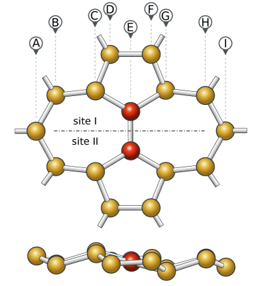
Next we investigate the effect of the presence of a SW-defect on substitutional nitrogen doping in silicene. As a result of local deformations induced by the creation of a SW-defect (Fig. 1(b)) every single Si atom in the surroundings of a SW-defect provides a unique place for substitution. Since the surrounding atoms still maintain their buckled hexagonal nature we will focus only on the Si atoms that are part of the heptagons or pentagons in the SW-defect. As a consequence of the lattice symmetry with respect to the Si-Si dimer at the defect core a similar behavior of adsorbates on site I and II can be expected. However, in order to not exclude the possible effects of lattice distortion on N substitution, calculations were performed for all 16 sites of the SW defect. Possible positions for substitutional doping with one substituent atom are displayed in Fig. 5. Additionally, we present structural properties, total magnetic moment, formation energies and binding energy values in Table 2.
The substitution positions can be divided into the four groups. The first group contains the lattice sites that belong to edges of heptagons A, B, H and I. We found that Si-N bonds at the edges of heptagons are not stable and hence the substitution of a N atom on A, B, H and I positions cannot be realized.
| defect site | |||||
|---|---|---|---|---|---|
| (Å) | (deg) | (eV) | (eV) | ||
| N @ pure silicene | 1.83 1.83 1.83 | 60.0 | 1.0 | 0.59 | -4.6 |
| N @ A,B,H,I | - - - | - | - | - | - |
| N @ C | 1.86 1.82 1.80 | 61.7 | 1.0 | 1.8 | -3.4 |
| N @ D | 1.78 1.82 1.80 | 61.5 | 0.7 | 1.1 | -4.0 |
| N @ E | 1.83 1.83 1.76 | 61.3 | 1.0 | 1.5 | -3.7 |
| N @ F | 1.80 1.78 1.82 | 61.5 | 0.7 | 1.1 | -4.0 |
| N @ G | 1.79 1.82 1.83 | 61.7 | 1.0 | 1.8 | -3.3 |
The second group is composed of C, and G substitution sites that locate at the outermost intersection of heptagons and the pentagons of the defect core. Though C and G sites are geometrically and energetically similar, because of the lattice distortion induced by N-doping and buckled nature of the silicene lattice, these adsorption sites are not identical. Similar to doping in perfect silicene the substitution of a N atom on C and G site result in spin polarization of 1 . The binding energies on these lattice sites are smaller compared to intrinsic silicene.
The third group of possible substitution points are I and II sides of E which are located in the middle of the defect core. Clearly, both sides of E are equal for N-doping. When a N atom is substituted over E site, the resulting structure has a total magnetic moment of 1 and doping on these sites is by 0.4 eV more favorable than doping on C and G sites.
The last group includes D and F substitution sites, which belong to the pentagons of the SW-defect. The Si-N bond lengths in these lattice sites are smaller or equal to the bond lengths in N-doped silicene. For those structures we also observe large rippling of the order of 2 Å. We found that substitutional doping on D and F positions does not give rise to a shrinkage of the lattice parameters. D and F points are energetically most favorable sites on a SW defect with a binding energy of eV. It is seen that nitrogen substitution results in a net magnetic moment of 0.7 . Similar to N-doping in perfect silicene, SW-defected silicene shows metallic behavior for all possible substitution sites that belong to the core of SW defect.
IV Conclusions
In this study we performed ab initio calculations in order to investigate the formation of SW defects in silicene and to show the effect of these defects on the reactivity of the silicene with respect to nitrogen doping. We found the formation of a SW-defect to be much easier in the buckled lattice structure of silicene as compared to graphene. The softer bonding nature of silicene allows easier formation of a SW defect with a smaller energy barrier for both free standing as well as supported silicene. The presence of a SW defect in silicene breaks the symmetry and results in a band gap opening in electronic band structure with size depending on the defect concentration. Additionally, our vibrational analysis reveals that the formation of SW defects in freestanding silicene inevitably leads to the formation of large ripples. Moreover, the presence of an underlying Ag(111) supporting surface increases the barrier for the formation of SW defects from 2.4 to 2.8 eV. We also found that the buckled nature of silicene provides a large energy barrier for healing of SW defect and therefore defective silicene is quite stable even at high temperatures.
Furthermore, the presence of SW defects significantly modifies the doping characteristics of silicene. While doping defect-free silicene by N atoms is favorable with a little lattice shrinking, the presence of a SW defect limits the number of possible doping sites. We found that all the nitrogen substitution sites on the defect core are less preferable than defect-free silicene. Among the possible sites of defect the edges of heptagons are least favorable sites while doping of the N atoms at the edges of pentagons is most preferable. Our findings on the reactivity of SW-defected silicene domains agree well with the very recent study that reports the chlorine adsorption on SW-defected graphene and carbon nanotube.mari We believe that our results provide a basis for the understanding of the characteristic properties of defected silicene which are essential for its utilization in future electronics.
Acknowledgements.
This work was supported by the Flemish Science Foundation (FWO-Vl) and the Methusalem foundation of the Flemish government. Computational resources were provided by TUBITAK ULAKBIM, High Performance and Grid Computing Center (TR-Grid e-Infrastructure), and HPC infrastructure of the University of Antwerp (CalcUA) a division of the Flemish Supercomputer Center (VSC), which is funded by the Hercules foundation. H.S. is supported by a FWO Pegasus Marie Curie Fellowship.References
- (1) K. S. Novoselov, A. K. Geim, S. V. Morozov, D. Jiang, Y. Zhang, S. V. Dubonos, I. V. Grigorieva, and A. A. Firsov, Science 306, 666 (2004).
- (2) S. V. Morozov, K. S. Novoselov, M. I. Katsnelson, F. Schedin, D. C. Elias, J. A. Jaszczak, and A. K. Geim, Phys. Rev. Lett. 100, 016602 (2008).
- (3) J. H. Chen, C. Jiang, S. Xiao, M. Ishigami, and M. S. Fuhrer, Nat. Nanotechnol. 3, 206 (2008).
- (4) A. A. Balandin, S. Ghosh, W. Bao, I. Calizo, D. Teweldbrhan, F. Miao, and C. N. Lau, Nano Lett. 8, 902 (2008).
- (5) C. Lee, X. Wei, J. W. Kysar, and J. Hone, Science 321, 385 (2008).
- (6) S. Cahangirov, C. Ataca, M. Topsakal, H. Sahin, and S. Ciraci, Phys. Rev. Lett. 108, 126103 (2012).
- (7) F. Banhart, J. Kotakoski, and A. V. Krasheninnikov, ACS Nano 5, 26 (2011).
- (8) R. Balog, B. Jorgensen, L. Nilsson, M. Andersen, E. Rienks, M. Bianchi, M. Fanetti, E. Laegsgaard, A. Baraldi, S. Lizzit, Z. Sljivancanin, F. Besenbacher, B. Hammer, T. G. Pedersen, P. Hofmann, and L. Hornekaer, Nat. Mater. 9, 315 (2010).
- (9) J. Lahiri, Y. Lin, P. Bozkurt, I. I. Oleynik, and M. Batzill, Nature Nanotech. 5, 326 (2010).
- (10) L. Tapasztó, G. Dobrik, P. Nemes-Incze, G. Vertesy, Ph. Lambin, and L. P. Biró, Phys. Rev. B 78, 233407 (2008).
- (11) A. V. Krasheninnikov and F. Banhart, Nat. Mater. 6 723 (2007).
- (12) M. H. Gass, U. Bangert, A. Bleloch, P. Wang, R. R. Nair, and A. K. Germ, Nat. Nanotechnol. 3, 676 (2008).
- (13) M. Topsakal, H. Sahin, and S. Ciraci, Phys. Rev. B 85, 155445 (2012).
- (14) A. J. Stone and D. J. Wales, Chem. Phys. Lett. 128, 501 (1986).
- (15) J. C. Meyer, C. Kisielowski, R. Erni, M. D. Rossell, M. F. Crommie, and A. Zettl, Nano Lett. 8, 3582 (2008).
- (16) Georgii G. Samsonidze, Guram G. Samsonidze, and B. I. Yakobson, Phys. Rev. Lett. 88, 065501 (2002).
- (17) C. P. Ewels et al., Chem. Phys. Lett. 351, 178 (2002).
- (18) J. Ma, D. Alfe, A. Michaelides, and E. Wang, Phys. Rev. B 80, 033407 (2009).
- (19) M. T. Lusk and L. D. Carr, Phys. Rev. Lett. 100, 175503 (2008).
- (20) Y. Li, J. C. Ren, R. Q. Zhang, Z. J. Lin, and M. A. Van Hove, J. Materi. Chem. 22, 21167 (2012).
- (21) L. Chen, H. Hu, Y. Ouyang, H. Z. Pan, Y. Y. Sun, and F. Liu, Carbon 49, 3356 (2011).
- (22) M. Ijäs, P. Havu, and A. Harju, Phys. Rev. B 87, 205430 (2013).
- (23) K. Takeda and K. Shiraishi, Phys. Rev. B 50, 14916 (1994).
- (24) S. Cahangirov, M. Topsakal, E Akturk, H. Sahin, and S. Ciraci, Phys. Rev. Lett. 102, 236804 (2009).
- (25) H. Sahin, S. Cahangirov, M. Topsakal, E. Bekaroglu, E Akturk, and S. Ciraci, Phys. Rev. B. 80, 155453 (2009).
- (26) P. Vogt, P. D. Padova, C. Quaresima, J. Avila, E. Frantzeskakis, M. C. Asensio, A. Resta, B. Ealet, and G. L. Lay, Phys. Rev. Lett.108, 155501 (2012).
- (27) B. J. Feng, Z. J. Ding, S. Meng, Y. G. Yao, X. Y. He, P. Cheng, L. Chen, and K. H. Wu, Nano Lett. 12, 3507 (2012).
- (28) A. Fleurence, R. Friedlein, T. Ozaki, H. Kawai, Y. Wang, and Y. Yamada-Takamura, Phys. Rev. Lett. 108, 245502 (2012).
- (29) Cheng-Cheng Liu, H. Jiang, and Y. Yao, Phys. Rev. B 84, 195430 (2011).
- (30) Cheng-Cheng Liu, W. Feng, and Y. Yao, Phys. Rev. Lett. 107, 076802 (2011).
- (31) N. D. Drummond, V. Zolyomi, and V. I. Fal’ko Phys. Rev. B 85, 075423 (2012).
- (32) M. Ezawa, Phys. Rev. Lett. 109, 055502 (2012).
- (33) H. Sahin and F. M. Peeters, Phys. Rev. B 87, 085423 (2013).
- (34) J. Sivek, H. Sahin, B. Partoens, and F. M. Peeters, Phys. Rev. B 87, 085444 (2013).
- (35) G. Kresse and J. Furthmuller, Comput. Mater. Sci. 6, 15 (1996).
- (36) G. Kresse and D. Joubert, Phys. Rev. B 59, 1758 (1999).
- (37) J. P. Perdew, K. Burke, and M. Ernzerhof, Phys. Rev. Lett. 77, 3865 (1996).
- (38) P. E. Blöchl, O. Jepsen, and O. K. Andersen, Phys. Rev. B 49, 16223 (1994).
- (39) H. J. Monkhorst and J. D. Pack, Phys. Rev. B 13, 5188 (1976).
- (40) H. Sahin and S. Ciraci, Phys. Rev. B 84, 035452 (2011).
- (41) S. Kattel, P. Atanassov, and B. Liefer, J. Phys. Chem. C 116, 8161 (2012).
- (42) L. S. Panchakarla, K. S. Subrahmanyam, S. K. Saha, A. Govindaraj, H. R. Krishnamurthy, U. V. Waghmare, and C. N. R. Rao, Adv. Mater. 21, 4726 (2009).
- (43) L. Zhao, R. He, K. T. Rim, T. Schiros, K. S. Kim, H. Zhou, C. Gutiérrez, S. P. Chpckalingam, C. J. Arguello, L. Pálová, D. Nordlund, M. S. Hybertsen, D. R. Reichman, T. F. Heinz, P. Kim, A. Pinczuk, G. W. Flynn, and A. N. Pasupathy, Science 333, 999 (2011).
- (44) X. R. Wang, X. L. Li, L. Zhang, Y. K. Yoon, P. K. Weber, H. L. Wang, J. Guo, and H. J. Dai, Science 324, 768 (2009).
- (45) D. C. Wei, Y. Q. Liu, Y. Wang, H. L. Zhang, L.P. Huang, and G. Yu, Nano Lett. 9, 1752 (2009).
- (46) Y. Fujimoto and S. Saito, Phys. Rev. B 84, 245446 (2011).