Large-aperture wide-bandwidth anti-reflection-coated silicon lenses for millimeter wavelengths
Abstract
The increasing scale of cryogenic detector arrays for sub-millimeter and millimeter wavelength astrophysics has led to the need for large aperture, high index of refraction, low loss, cryogenic refracting optics. Silicon with , low loss, and relatively high thermal conductivity is a nearly optimal material for these purposes, but requires an antireflection (AR) coating with broad bandwidth, low loss, low reflectance, and a matched coefficient of thermal expansion. We present an AR coating for curved silicon optics comprised of subwavelength features cut into the lens surface with a custom three axis silicon dicing saw. These features constitute a metamaterial that behaves as a simple dielectric coating. We have fabricated and coated silicon lenses as large as 33.4 cm in diameter with coatings optimized for use between 125-165 GHz. Our design reduces average reflections to a few tenths of a percent for angles of incidence up to with low cross-polarization. We describe the design, tolerance, manufacture, and measurements of these coatings and present measurements of the optical properties of silicon at millimeter wavelengths at cryogenic and room temperatures. This coating and lens fabrication approach is applicable from centimeter to sub-millimeter wavelengths and can be used to fabricate coatings with greater than octave bandwidth.
pacs:
000.2190, 220.0220, 110.0110, 310.1210, 080.2208, 220.3630, 120.4570, 120.4610, 160.1245, 230.4170I Introduction
The development of large format superconducting detector arrays for millimeter and sub-millimeter astrophysics (e.g. Bintley:2012 ; Niemack:2008 ; Padin:2008 ) has driven the need for high-throughput optical designs that maintain diffraction limited performance across the arrays (see Hanany:2012 for a review). Silicon is an excellent material for these applications due to its high index of refraction (), low loss-tangent (tan ), and a relatively high thermal conductivity ( 200 at 4 Thompson:1961 , which is only a factor of 50 lesser than high quality OFHC copper Sciver:2012 and orders of magnitude higher than plastic). The essential development required to realize optical designs using silicon optics at millimeter wavelengths is an appropriate anti-reflection (AR) coating to mitigate the 30% (-5 dB) reflective loss from each optical surface.
AR coatings consist of one or more dielectric layers placed on the surface of refractive optical elements. The index of refraction and thickness of the AR layers are chosen such that the reflections from the vacuum-AR interface and from the AR-substrate interface interfere and cancel. If the optical path length through a single layer AR coating is one quarter wavelength, the refractive index of the coating is (where is the index of the substrate), and the coating is free from dielectric losses, the cancelation is perfect at one particular frequency. Applied to silicon, such quarter-wave coatings reduce reflections below over 1.25:1 bandwidth at normal incidence.
Wider bandwidths and larger ranges of angles of incidence can be accommodated by adding additional layers to the AR coating to form a multi-layer coating. These coatings require layers with a number of different refractive indices. Cryogenic applications require that the coefficient of thermal expansion of the AR layers also be sufficiently matched to that of the lens substrate to prevent damage upon cooling. The dielectric loss and birefringence of the AR coating material must also be carefully controlled. Locating materials with these properties poses a significant challenge to implementing cryogenic wide band AR coatings for silicon. One avenue to solve this problem is to engineer materials with the required dielectric constant by cutting sub-wavelength features into the lens surface Collin:1990 ; Smith:2006 . Engineered optical materials with properties determined by their detailed geometric shape, size and orientation are referred to as artificial dielectrics or metamaterials.
Simulated dielectric metamaterial AR coatings consist of layers of sub-wavelength holes Kildal:1984 , posts, or grooves Cohn:1961 cut into the substrate to be coated. This approach allows the index of the AR coating to be precisely tuned by adjusting the geometry of the machined features, naturally solves the thermal expansion problem, and has loss lower than that of the substrate. At cryogenic temperatures silicon has a dielectric loss tangent 100 times lower than typical plastics like Cirlex, which have previously found use as single layer AR coatings Lau:2006 . The advantages of silicon metamaterial AR coatings include precisely controlled indices of refraction, inherently matched thermal expansion, and significantly reduced dielectric losses.
This approach has been successfully applied to plastic millimeter wave optics through direct machining and silicon optics for visible wavelengths through patterning of geometric structures which perform as a AR coating similar to that found on a moth’s eye Thornton ; Chapham ; Motamedi . At millimeter wavelengths Zhang et al. Zhang:2009 fabricated an alternative class of simulated dielectric AR for silicon composed of metal resonant structures supported by a plastic substrate that had higher losses than the coating described here. Schuster et al. Schuster:2005 fabricated single layer silicon micro-machined artificial dielectrics and Han et al. Han:2010 have used silicon immersion grating technology to fabricate planar artificial dielectrics for THz radiation. Our work is the first demonstration of a broad-bandwidth metamaterial AR coating on silicon optics with finite curvature for millimeter wavelengths.
The AR coated lenses presented here have been developed for the ACTPol Niemack:2010 project, a polarization sensitive receiver for the Atacama Cosmology Telescope (ACT, Fowler:2007 ). In Section II we present the design requirements for the ACTPol optics as they apply to this work. The design of the coating is described in Section III. In Section IV we describe the ACTPol lens design. Cryogenic measurements of the dielectric properties of silicon samples taken from 45 cm diameter ingots at millimeter wavelengths are presented in Section V. In Section 8 we describe the fabrication process of the coating on the lenses and present reflection measurements of a finished lens. We conclude with a brief discussion of the range of applicability of this coating technique.
II Requirements
The performance requirements for the AR coated silicon lenses described in this work are dictated by the scientific goals of the ACTPol project Niemack:2010 . This instrument is designed to detect the faint polarized signals from the cosmic microwave background using three detector arrays fed by independent re-imaging optics. Two of the arrays are horn coupled polarimeters for the 150 GHz band (passband from 125 to 165 GHz), while the third array will be a multichroic array including both 150 GHz and 90 GHz bands (‘90 GHz’ passband from 80 to 110 GHz) McMahon:2012 . Extensive design studies demonstrated high index of refraction ( ) lenses were needed to achieve high optical quality across the required field of view.
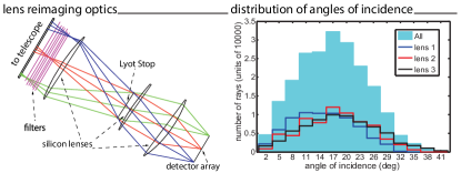
In this paper we focus on the coatings for the 150 GHz band lenses. These coatings are conceptually similar to those which will be used for the broader-band multichroic lenses. The bandwidth requirement for the 150 GHz band coatings is to have transmission between 125 and 165 GHz. The left panel of Figure 1 shows the re-imaging optics for a 150 GHz array. The optics include three plano-convex silicon lenses with diameters up to 33.4 cm. The figure shows that rays passing through the optical system refract over a wide range of angles of incidence. This is quantified in the right hand panel of Figure 1 which shows that the distribution of angles of incidence is centered near and that more than 96% of the rays have angles of incidence . This sets the requirement that the coatings must be optimized to minimize reflections for angles of incidence between and .
Since ACTPol is a polarization sensitive experiment, low cross-polarization is another requirement. Studies of polarization systematics (e.g., Shimon:2008 ) suggest that the CMB temperature to polarization leakage must be controlled to better than which corresponds to a requirement that differences in the transmission for the two polarizations be 0.5%.
To reduce the thermal emission, all optics are cooled to 4K or below. Thus the AR coating must be able to withstand cryogenic cycling.
As described in §V high resistivity silicon which is available in boules up to 45 cm in diameter, offers a cryogenic loss tangent , an index of refraction of , and a relatively high thermal conductivity making it an ideal material for this optical design. Our approach of directly machining metamaterial AR coatings into the lens surfaces guarantees that the coatings have low dielectric losses and coefficients of thermal expansion that are inherently matched to that of the silicon lenses.
III AR Coating Design
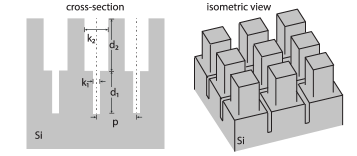
The AR coating is comprised of two metamaterial layers. Each layer consists of an array of square pillars on a square grid cut using silicon dicing saw blades by making two sets of parallel trenches rotated relative to each other. It has been shown that any electromagnetic structure with an axis of n-fold (n2) rotational symmetry must have polarization independent reflectance and zero cross-polarization when light is incident along this axis Mackay:1989 . Hence the rotational symmetry of this coating leads to zero cross-polarization at normal incidence and low birefringence at oblique incident angles. Figure 2 shows a cross-section and isometric view of this geometry which is parameterized by the depths , , and kerf widths , of the inner and outer layer respectively and a pitch . The outer layer is cut by using a blade of width and the inner layer is cut by making a second set of cuts to greater depth with a thinner blade of width . We introduce the volume fill factor to facilitate comparison to published analytic calculations based on the second order effective medium theory developed by Rytov Rytov:1956 for the effective dielectric constant in the quasi-static limit () Motamedi ; Biber:2003 ; Brundrett:1994 ; Gaylord:1986 .
The metamaterial layers can be treated as a volume distribution of small electromagnetic scatterers characterized by electric and magnetic polarizability densities Collin:1990 . When the pitch is small compared to shortest wavelength of interest, the fields in the layer are homogenous Smith:2006 and one can define an effective dielectric constant which can be used to parameterize the propagation properties of the media. This effective dielectric function for the layer, , is a function of the density of scatterers in the layer Aspnes2:1982 ; Aspnes1:1982 , parametrized by the volume fill factor. As the feature size of a composite media approaches a significant fraction of the radiation wavelength the effective dielectric function becomes frequency dependent Egan:1982 . As the wavelength is further reduced the artificial dielectric structure no longer appears homogenous and these simple quasi-static considerations must be augmented to adequately model its behavior. In going beyond the quasi-static limit resonant effects, diffraction and scattering can occur in the artificial dielectric structure Kildal:1984 ; Gentner:2006 ; Raguin:1993 ; Matthaei . The coatings described here, which operate between the quasi-static and diffractive regimes, rely on numerical simulations to estimate the relation between the volume fill factor and the effective refractive index of the metamaterial layer.
The values of , , , , and were chosen using a three step design process. A preliminary design was carried out using a classical analytic model consisting of sheets of dielectric material each with a constant thickness and index of refraction Jackson:1998 . These were varied to minimize the reflectance across the band yielding targets for the electrical thickness and index of refraction of our two layer coating.
The second step was to translate the index and thickness from the simple model into the pitch, kerfs and depths for our coating geometry. This step required knowledge of the relation between the effective index of refraction of an array of square pillars and the pitch and kerf of that layer. These relations were determined by fitting analytic models to HFSS (High Frequency Structure Simulator, Ansoft:HFSS ) simulations of single layer coatings with a wide range of volume fill factors for a few different choices of pitch. The HFSS simulations were carried out using Floquet ports and master-slave boundary conditions to model a box containing a single post of the AR coating as an infinite periodic two dimensional array of features Ansoft:HFSS .
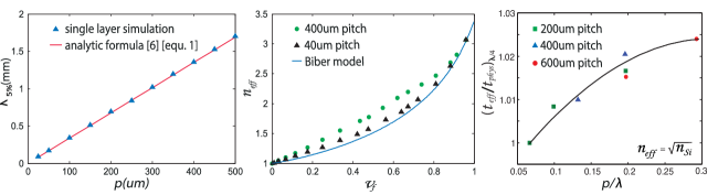
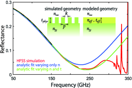
Figure 3 shows a representative simulation of a single layer pillar geometry with insets showing the simulated geometry and the simple dielectric layer modeled in the fit. The fit constrained the effective index , the effective electrical thickness and the maximum frequency to which our metamaterial coating behaves as a simple dielectric. For the purposes of our fit we define this maximum frequency as the point where the simulated reflectance and the analytic fit disagree at more than 5% absolute reflectance. We refer to this frequency as and the corresponding wavelength . This indicates the transition between specular and diffractive behavior of the coating.
A second fit which fixed the electrical thickness to the physical thickness of the pillars is also shown in Figure 3. This fit implies a lower . The discrepancy between the best fit thickness and the physical thickness of the metamaterial layer arises since the geometric structure of the pillars results in fringing of fields at the junction between layers causing a perturbative shift between the position of the physical interface and the effective location of the junction’s electrical reference plane. An analogous effect is encountered in the design of metallic waveguide structures Matthaei , which can be analytically treated.
Figure 4 shows the results from fitting a number of HFSS simulations with different pitch and fill factor to the analytic model. Plots include the breakdown wavelength , the effective index , and the electrical thickness of a layer with index expressed as a ratio of the thickness of a quarter wave homogenous dielectric layer and a quarter wave metamaterial layer.
The recovered is in good agreement with the analytic condition derived for a silicon optic in vacuum Kildal:1984 ; Raguin:1993 to prevent diffraction from a grating array,
| (1) |
where is the pitch, is the wavelength, is the index of silicon, and is the angle of incidence. This analytic expression shows that the pitch must be smaller than implied by the calculated at normal incidence to minimize diffraction at oblique angles of incidence. Consideration of manufacturing cost and mechanical robustness of the two-layer AR coating design favors the largest possible pitch, as this choice minimizes the number of cuts required to cover a given area and makes the pillars larger and therefore stronger. A 435 m pitch leads to acceptable performance up to GHz ( mm) which is the upper edge of our band.
Comparing this relation between and to analytic models Biber:2003 ; Motamedi for the case where the electric field of the incident wave is perpendicular to the grooves, we found discrepancies that are reduced as the pitch decreases and we approach the quasi-static limit . Given that our coating design does not operate in this limit we find the analytic models insufficiently accurate for our purposes. Thus we resort to numerical simulation to optimize the geometry of our coating.
The variation in the electrical thickness compared to the physical thickness (Figure 4, right) is shown for the case of a quarter wave AR coating with index . Additional simulations show that the electrical thickness depends on the index of refraction of the material on either side of the metamaterial dielectric layer. We account for this small effect in the final numerical optimization of the multilayer coating design.
| parameter | symbol | dimension | dimension |
|---|---|---|---|
| (m) | (units of ) | ||
| pitch | |||
| kerf* | |||
| depth | |||
| volume fill factor* | 1 | ||
| 2 |
* nominal average values
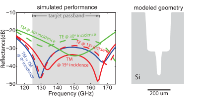
With these relations (Figure 4) in hand we convert the analytic design of our two layer coating into parameters for the pillar geometry. In the final step we performed a numerical optimization of the coating at angle of incidence using HFSS, with the constraint that the cut geometry must match the kerf geometry of commercially available dicing saw (See Section 8). This step enables manufacturability, accounts for any discrepancies between the electrical and physical thickness implied by our numerical simulations, and improves the performance at larger angles of incidence. Table 1 gives the parameters for the resultant design and Figure 5 shows the simulated performance for this coating as a function of frequency for several (, and ) angles of incidence. Even at incidence the band averaged reflections are at dB and differences between the two linear polarization states (TE and TM, see Jackson:1998 for definition) are below 0.5% for all frequencies and angles. At incidence, average reflections are below dB. The tolerance of the design to various possible manufacturing errors are described in detail in Appendix A.
IV ACTPol Lenses
The ACTPol lenses are cylindrically symmetric plano-convex designs in which the convex surface is aspheric - a conic section with four perturbing terms proportional to the fourth, sixth, eighth, and tenth order of the distance from the axis. The design optimization procedure for the re-imaging optics is similar to that described in Fowler:2007 ; the primary difference being that the ACTPol optics are required to be image-space telecentric to optimize the coupling to the flat feedhorn arrays. This was accomplished by constraining the chief rays at each field point to be near normal incidence at the focal plane and by allowing the tilts of lens 2, lens 3, and the focal plane to vary during the optimization. The resulting design achieves Strehl ratios greater than 0.93 across the 150 GHz focal planes without accounting for the Gaussian illumination of the feedhorns, which effectively improves the image quality. All three of the ACTPol optics tubes use the same three silicon lens designs with the positions and tilts adjusted to optimize the coupling to the ACT Gregorian telescope Fowler:2007 .
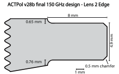
The AR coating approach we have developed constrains the perimeter of the lens designs to enable accurate clamping during both machining of the AR coatings and cryogenic cycling of the lenses. Figure 6 shows a cross-section of the perimeter of an ACTPol lens design. Each lens includes a handling ring along its perimeter that is not AR coated and is used for mounting the lens during machining as well as clamping to cool the lens in the cryogenic receiver. The outer corners of the perimeter are chamfered to minimize chipping. There are steps rising from the perimeter to the lens surface to provide clearance between the perimeter clamping region and the AR coating. The lens blanks were machined by Nu-Tek Precision Optical Corporation and achieved 5 m tolerances.
V Properties of Silicon
Silicon manufacturing can produce different grades of material, such as ultra high purity silicon produced by the float zone process Duffar that has a negligible density of impurities and silicon produced by the Czochralski process Duffar that has a higher level of impurities. As charge carriers and associated states introduced by impurities are the cause of dielectric loss, use of the highest available purity (as inferred from the room temperature resistivity) silicon minimizes the dielectric losses. Measurements of the refractive index, dielectric permittivity and loss tangent of various high purity and high resistivity silicon sample over a range of frequencies and temperature have been reported Krupka:2006 ; Afsar:1994 ; Parshin:1995 . For example, ultra high purity silicon has been measured to have a loss tangent of at room temperature which would correspond to loss in the ACTPol optical system. Unfortunately, surface tension limits the zone-melt purification technique used to produce ultra high purity silicon to diameters below about 200 mm. Therefore, the substrates available for large diameter lenses considered in this work must be fabricated from Czochralski silicon. For our low temperature application we expect the bulk conductivity of silicon to freeze out dramatically reducing the dielectric losses, however, other loss mechanisms can persist in the desired design band. We validate this general picture of the dielectric loss in silicon by optically characterizing the influence of the bulk resistivity as a function of frequency and sample temperature.
Samples produced by the Czochralski process and readily available in 450 mm diameter stock with bulk resistivities specified to be in the range of 1 to -cm were characterized both at room temperature and 4K using a Bruker 125 high-resolution Fourier Transform Spectrometer (FTS) with a Oxford Cryostat CF continuous liquid helium flow sample chamber. The cryostat is equipped with pair of 75m thick polypropylene windows that enable spectral measurement while allowing the sample to be held at a regulated temperature. The samples were cut to have a typical thickness of m, double side polished, and placed in a 25 mm diameter optical test fixture at the focus of an beam. The reflections from the two surfaces of the sample form a Fabry-Perot resonator for which the modeling is relatively simple permitting measurement of dielectric properties. The silicon samples are boron doped (p-type) to adjust the resistivity. The -cm resistivity silicon used in the ACTPol lenses has the minimum dopant level.
Each sample’s transmission was measured between GHz ( icm) and THz ( icm) using different combinations of sources, beam splitters, and detectors for three frequency bands between 240-450GHz (8-15 icm), 450-2850 GHz (15-95 icm), and 2.85-18 THz (95-600 icm).
The spectral resolution employed, 7.5 GHz (0.25 icm), fully resolves the sample’s spectral features. Sliding stages permit the sample or a reference clear aperture to be moved into the FTS beam while in the cryostat for in situ calibration.
The transmission spectrum was modeled as a series of homogeneous plane parallel dielectric layers Yeh . The dielectric function for the silicon was approximated by a classical Drude dispersion model Button :
| (2) |
where is a complex function of frequency , the damping rate , and the contribution to the relative permittivity of higher energy transitions. The plasma frequency and the damping rates are related by, , where is the permittivity of free space and is the sample’s bulk resistivity VanExter . In this approximation, the material’s free carriers are treated as classical point charges undergoing random collisions and the resulting damping is assumed to be independent of the carrier energy. We find this representation suitable to represent the sample’s properties over the spectral and temperature ranges of interest.
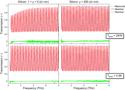
The sample thickness is known to m at room temperature and corrected for thermal contraction as a function of temperature Okada . Since the fringe rate is proportional to the product of the refractive index and sample thickness,uncertainties in the sample thickness directly limit the precision of the determination of . Measurements of an optically polished crystalline quartz sample with accurately known thickness were used to measure a 1% amplitude uncertainty across the entire FTS band. This calibration uncertainty leads to a corresponding reduction in the measurement’s sensitivity to . These uncertainties were accounted for in fitting the FTS data. These fits produced root-mean-square deviations in the range of 0.005-to-0.016 between the model and the observation spectra. Representative data for the and -cm samples are shown in Figure 7 for sample physical temperatures of =297 and 4.5 K.
| -cm | [K] | THz | THz | ||
|---|---|---|---|---|---|
| 500 | 297 | 11.7(1) | 0.0015 | ||
| 4.5 | 11.5(5) | 0.0008 | |||
| 1-to-5 | 297 | 11.6(55) | 0.0046 | 0.571 | 1.60 |
| 200 | 11.5(52) | 0.0049 | 0.572 | 0.80 | |
| 100 | 11.4(78) | 0.0028 | 0.459 | 0.26 | |
| 70 | 11.4(66) | 0.0011 | 0.162 | 0.20 | |
| 30 | 11.4(64) | 0.0008 | |||
| 10 | 11.4(62) | 0.0008 | |||
| 4.5 | 11.4(62) | 0.0008 |
The results of these fits are shown in Table 2. As anticipated the finite plasma frequency and damping rate contribute significantly to the room temperature losses, however, the -cm sample could be approximated by a dielectric constant over the spectral range of interest (e.g., and are consistent with zero). The influence of free carrier collisions at room temperature on the optical response becomes more pronounced in the -cm sample, manifesting as a reduction in transmission at low frequencies. However, as the -cm sample is cooled, bulk conduction is suppressed and this effect shifts to lower frequencies than of interest for millimeter wave applications. The observed dielectric parameters are a weak function of temperature below K as anticipated given exponential thermal dependance of the bulk resistivity Shklovskii .
Both samples show shifts in the magnitude of the index of refraction () upon cooling. This shift is accounted for in our optical design. At low temperature both the high and low resistivity sample give an upper limit for the loss tangent of For the ACTPol optics at 150 GHz, this corresponds to an absorptive loss of for our optical system comprising three lenses. The ACTPol lenses were fabricated from -cm silicon as it may reduce loss and facilitates room temperature testing. Both high and low resistivity silicon would provide acceptable performance in 4K cryogenic applications, but given the small cost differential high resistivity silicon is the natural choice. Although we have used high-resistivity silicon, our models and observations suggest that the carriers will be frozen out at 4K for the range of bulk resistivities considered here. We note that the conductivity of silicon at room temperature, and therefore the loss, is a strong function of UV irradiance. We have not investigated this dependence cryogenically.
VI Coating Fabrication
The coatings were fabricated using silicon dicing saw blades which are available in widths ranging from 10 to hundreds of microns. Mounted on a commercial silicon dicing saw machine these blades repeatedly cut with micron level precision and cutting speeds up to several centimeters per second. Unfortunately, commercial silicon dicing machines are not designed for curved surfaces and cannot accommodate the large diameter lenses required for this project. Therefore we constructed a custom three axis silicon dicing system to fabricate these coatings.
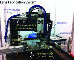
The fabrication system is shown in Figure 8. It consists of a micron accurate three axis stage on which we mount an air bearing dicing spindle and a micron accurate depth gauge. The spindle and retractable depth gauge are attached to the vertical stage (Z-axis) which rides on the horizontal (Y-axis) stage. A lens is mounted on an aluminum mounting plate on a horizontal stage (X-axis) below the spindle. This plate permits the lens to be rotated by , , , and and carries a reference wafer that is used in setting up the blades prior to cuts. A side looking microscope is mounted parallel to the Y-axis to characterize test cuts on the reference wafer. Flood cooling water is sprayed on the dicing blade while cuts are made to carry away debris. A temperature controlled water bath is used to regulate the temperature of the spindle and maintain the flood coolant and air surrounding the dicing system within C.
Our system does not show any appreciable change in cut shape or surface damage when cutting at the maximum travel speed of 50 mm/s. We conservatively operate at 25 mm/s for which it takes a total of 12 hours of machining per lens side. Factoring in setup time it takes 6 8-hour days to fabricate a single lens.
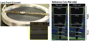
Figure 9 shows photographs of one of the ACTPol AR coated silicon lenses. The fabricated coating is sufficiently robust to permit handling the lenses by touching the AR coatings. The manufacture resulted in less than 10 out of 500,000 posts with damage visible by eye. The shape of the cut profiles was evaluated by making cuts on a reference silicon wafer before cutting (pre-cut) and after cutting (post-cut) the lens and measuring them using the side looking microscope. Comparison of the pre-cut and post-cut measurements (See Figure 9) show that the wide blade cuts repeatably with negligible evolution to cut profile while the the narrow blade shows some evolution in width in the upper third of the cut. Simulations show that this evolution, leads to a few tenths of a percent increase in the reflectance. The accuracy of the depths of the cuts is limited by a 3 micron uncertainty in the zero point for the blade depth and a micron quadruple warp in the lens. This warp is due to imperfections in the lens mounting plate that stress the lens.
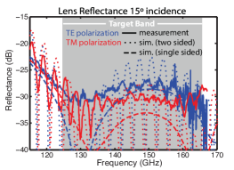
The reflectance of the completed ACTPol lenses were measured using a scalar reflectometer. This reflectometer consisted of a tunable narrow band continuous wave source which illuminated the flat side of lens through a full width half power horn, from a distance of 5 cm, and tilted at an angle of relative to the lens surface normal. A receiver consisting of an identical horn coupled to a detector diode was placed at the mirror image of the source horn relative to the plane defined by the point of maximum illumination of the lens and perpendicular to a line joining the source and receiver. This system was calibrated by (1) placing an aluminum reflector at the same position as the lens to normalize the peak reflection to unity, and (2) by removing the lens and calibration reflector to measure the stray reflections which were found to be negligible.
The results of this reflectance measurement are shown in Figure 10 for both the TE and TM polarizations. Precise modeling of this measurement configuration requires accounting for the interference between reflections from the flat and curved lens surface, which is beyond the scope of this work. However, the results are expected to be intermediate between the reflectance from a single AR coated surface (single sided) and the easily simulated result for two flat surfaces separated by the central thickness of the lens (two sided). These two cases are presented in Figure 10 for both linear polarization states. These simulations incorporate the measured cut profiles shown in Figure 9. We empirically found that moving the lens so that it is well centered on the beam increases the interference effects (TM case) while moving the lens off center reduces these effects (TE case). Based on the reasonable agreement between these simplistic simulations and the measurement we are confident we are reducing reflections to a few tenths of a percent over the range of angles of incidence required for ACTPol.
VII Conclusion
We have described a new approach for AR coating silicon lenses over broad bandwidths and a range of angles of incidence. Simulations, backed up by measurements of an AR coated lens, show that the fabricated coating of the lenses presented here can reduce reflections below few tenths of a percent between 125 and 165 GHz for angles of incidence between 0 and for cryogenic applications. We have developed a micron-accurate 3-axis silicon dicing saw facility and are using it to manufacture AR coated lenses for ACTPol. We have also shown that a range of p-type silicon doping levels can achieve low loss at cryogenic temperatures using silicon samples from boules as large as 45 cm diameter. This approach for implementing wide-bandwidth AR coated silicon lenses is applicable for millimeter and sub-millimeter wavelength ranges and can be expanded to wider bandwidth by adding additional layers to the AR coating.
Acknowledgement
This work was supported by the U.S. National Science Foundation through awards AST-0965625 and PHY-1214379 and NASA through the NASA Space Technology Research Fellowship training grant NNX12AM32H. The authors would like to thank Ki Won Yoon and Molly Dee for useful discussions.
References
- (1) D. Bintley et al., “Commissioning SCUBA-2 at JCMT and Optimising the Performance of the Superconducting TES Arrays”, Journal of Low Temperature Physics, 167, 152-60 (2012).
- (2) M.D. Niemack et al., “A Kilopixel Array of TES Bolometers for ACT: Development, Testing, and First Light”, Journal of Low Temperature Physics, 151, 690-6 (2008).
- (3) S. Padin et al., “South Pole Telescope optics”, Applied Optics 47, 4418-28 (2008).
- (4) S. Hanany, M. D. Niemack, and L. Page, “CMB Telescopes and Optical Systems”, Planets, Stars and Stellar Systems, Volume 1: Telescopes and Instrumentation (arXiv:1206.2402, in press).
- (5) J. C. Thompson and B. A. Younglove, “Thermal Conductivity of Silicon at Low Temperatures”, J. Phys. Chem. Solids, Pergamon Press 1961. Vol. 20, Nos. 1/2, pp. 146-149.
- (6) S. W. Va Sciver, Helium Cryogenics, International Cryogenics Monograph Series, Springer Science+Business Media, LLC 2012, ch. 2.
- (7) R.E. Collin, Field Theory of Guided Waves, 1990, McGraw-Hill, McGraw-Hill, New York, pp. 749-786.
- (8) D.R. Smith and J.B. Pendry, “Homogenization of metamaterials by field averaging (invited paper)”, March 2006, Journal of the Optical Society of America B, Vol. 23, No. 3, pp. 391-403.
- (9) P.-S. Kildal, K. Jakobsen, and K. Sudhakar Rao, “Meniscus-lens-corrected corrugated horn: a compact feed for a Cassegrain antenna,” IEE Proc. 131, 390-4 (1984).
- (10) Cohn S. B., “Lens Type Radiators: Antenna Engineering Handbook”, 1961 (McGraw-Hill, N.Y.)
- (11) J. Lau et al., “Millimeter-wave antireflection coating for cryogenic silicon lenses”, Applied Optics, 45, 3746-51 (2006).
- (12) P.B. Clapham and M.C. Hutley, “Reduction of Lens Reflection by ‘Moth Eye’ Principle”, 1973, Nature, Vol. 244, pp. 281-282.
- (13) B.S. Thornton, “Limit of the moth’s eye principle and other impedance-matching corrugations for solar-absorber design”, 1975, Journal of the Optical Society of America, Vol. 65, No. 3, pp. 267-270.
- (14) M.E. Motamedi, W.H. Southwell, and W.J. Gunning, “Antireflection surfaces in silicon using binary optics technology”, 1992, Applied Optics, Vol. 31, No. 22, pp. 4371-4376.
- (15) J. Zhang, et al., “New artificial dielectric metamaterial and its application as a terahertz antireflection coating”, Applied Optics, 48, 6635 (2009).
- (16) K.-F. Schuster, et al. “Micro-machined Quasi-Optical Elements for THz Applications”, Sixteenth International Symposium on Space Terahertz Technology, held May 2-4, 2005 at Chalmers University of Technology. G teborg, Sweden., p. 524-528.
- (17) P. Han et al., “Application of Silicon Micropyramid Structures for Antireflection of Terahertz Waves”, IEEE Journal of Selected Topics in Quantum Electronics, Vol. 16, No. 1, January/February 2010
- (18) M.D. Niemack, et al., “ACTPol: a polarization sensitive receiver for the Atacama Cosmology Telescope”, Proc. SPIE 7741 (2010), arXiv:1006.5049.
- (19) J.W. Fowler, et al., “Optical design of the Atacama Cosmology Telescope and the Millimeter Bolometric Array Camera”, Applied Optics 46, 3444-54 (2007).
- (20) J.J. McMahon, et al., “Multi-chroic Feed-Horn Coupled TES Polarimeters”, Journal of Low Temperature Physics, 167, 879-84 (2012).
- (21) M. Shimon et al., “CMB Polarization Systematics due to Beam Asymmetry: Impact on Inflationary Science”, Phys. Rev. D77:083003 (2008).
- (22) A. MacKay, “Proof of Polarization Independence and Nonexistence of Crosspolar Terms for Targets Presenting n-Fold (n 2) Rotational Symmetry with Special Reference to Frequency-Selective Surfaces, 1989, Electron. Lett., vol. 25, no. 24, pp. 1624-1625.
- (23) S. Rytov, “The electromagnetic properties of finely layered medium”, Soviet Physics JETP 2 (1956) 466-475.
- (24) S. Biber, et al., “Design of Artificial Dielectrics for Anti-Reflection-Coatings”, 33rd European Microwave Conference, Munich (2003).
- (25) D.L. Brundrett, E.N. Glytsis, and T.K. Gaylord, “Homogeneous layer models for high-spatial-frequency dielectric surface-relief gratings: conical diffraction and antireflection designs”, 1 May 1994, Applied Optics, Vol. 33, No. 13, pp. 2695-2706.
- (26) T.K. Gaylord, W.E. Baird, and M.G. Moharam, “Zero-reflectivity high spatial-frequency rectangular-groove dielectric surface-relief gratings”, 15 December 1986, Applied Optics, Vol. 25, No. 24, pp. 4562-4567.
- (27) D.E. Aspnes, “Local-field effects and effective-medium theory: A microscopic perspective”, Am. J. Phys. 50, 704 (1982).
- (28) D.E. Aspnes, “Bounds on Allowed Values of the Effective Dielectric Function of Two-Component Composites at Finite Frequencies , 1982, Physical Review B, Vol. 25, No. 2, pp. 1358-1361.
- (29) W.G. Egan and D.E. Aspnes, “Finite-wavelength effects in composite media”, 1982, PRB, Vol. 26, No. 10, pp. 5313-5321.
- (30) A. Wagner-Gentner, et al. “Low loss THz window”, Infrared Physics and Technology 48 (2006) 249-253
- (31) G. Matthaei, L. Young, E.M.T. Jones, Microwave Filters, Impedance-Matching Networks and Coupling Structures, 1964, McGraw-Hill, New York, pp. 300-304.
- (32) D.H. Raguin and G.M. Morris, “Analysis of antireflection-structured surfaces with continuous one-dimensional surfaces profiles”, 10 May 1993, Applied Optics, Vol. 32, No. 14, pp. 2582-2598.
- (33) Jackson J.D., Classical Electrodynamics, 1998, John Wiley & Sons Inc.
- (34) “Ansoft High Frequency Structure Simulator (HFSS) software package”, http://www.ansys.com/Products/Simulation+Technology/Electromagnetics/High-Performance+Electronic+Design/ANSYS+HFSS
- (35) T. Duffar, Crystal Growth Processes Based on Capillarity: Czochralski, Floating Zone, Shaping and Crucible Techniques, (Wiley, Blackwell, 2010).
- (36) J. Krupka, et al., “Measurements of Permittivity, Dielectric Loss Tangent, and Resistivity of Float-Zone Silicon at Microwave Frequencies”, 2006, IEEE Transaction on Microwave Theory and Techniques, vol. 54, No. 11, pp. 3995-4000.
- (37) M.N. Afsar and H. Chi, “Millimeter wave complex refractive index, complex dielectric constant, and loss tangent of extra high purity and compensated silicon”, 1994, International Journal of Infrared and Millimeter Waves, vol. 15, pp. 1181-1188.
- (38) V. V. Parshin, et al. “Silicon as an Advanced Window Material for High Power Gyrotrons”, 1995, Int. Journal of Infrared and Millimeter Waves, vol. 16, no. 5, pp. 863-877.
- (39) P. Yeh, Optical Waves in Layered Media (Wiley, New York, 1988).
- (40) F. Gervais, “High-Temperature Infrared Reflectivity Spectroscopy by Scanning Interferometry” in Electromagnetic Waves in Matter, Part I, Vol. 8 (Infrared and Millimeter Waves), K. J. Button, eds. (Academic Press, London, 1983), pp. 284–287.
- (41) M. Van Exter and D. Grischkowsky, “Optical and Electronic Properties of Doped Silicon from 0.1 to 2 THz”, 1990, Applied Physics Letters, Vol. 56, No. 17, pp. 1694-1696.
- (42) Y. Okada and Y. Tokumaru, “Precise determination of lattice parameter and thermal expansion coefficient of silicon between 300 and 1500K”, 1984, J. Appl. Phys., Vol. 56, No. 2, pp. 314-320.
- (43) B.I. Shklovskii and A.L. Efros, Electronic Properties of Doped Semiconductors, 1984, Berlin, Germany, Springer, ch. 4.
Appendix A Tolerances
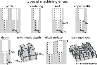
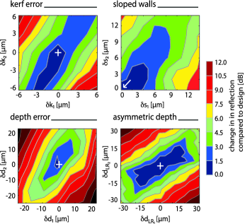
The manufacturing tolerances for the eight types of machining errors shown in Figure 11 were evaluated based on a fiducial design. These include: (1) errors in the pitch, ; (2) errors in the centering of the deeper groove relative to the shallow groove, ; (3) errors in the kerf widths, , ; (4) slopes in the walls of the grooves parameterized by and which represent the distance the upper and lower groove tilt inward at the groove bottom if the mean width is fixed; (5) errors in the depth of either grooves , , (6) differences in the depth of grooves in the two orthogonal directions assuming the correct mean depth are parameterized for the upper and for the lower groove; (7) application of this coating to a surface tilted at an angle relative to the bottom edge of the saw and where the depth of each groove is measured at the center of the groove (e.g., the effect of applying this coating at the edge of a curved lens); and (8) rows of broken posts. The tolerance to variation in the refractive index of the silicon substrate, was also evaluated. The tolerances for these parameters were quantified based on a fiducial model similar to what was fabricated but with straight walled pillars using HFSS simulations in which the parameters in each family were varied separately. For the majority of these effects the results were distilled to a band averaged reflection at angles of incidence. The sensitivity to each parameter was quantified as the displacement needed to bring about a dB increase in reflectance. For the case of tilted surface and for broken posts the results of a small number of simulations were evaluated and compared to the fiducial performance. In the remainder of this section we discuss these results.
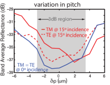
Pitch:
Variations in the pitch change the effective index of both layers. Figure 12 shows the band averaged reflectance as function of variation in the pitch. A conservative tolerance of m () limits the change in reflectance to be less than 3 dB.
Centering:
The performance was insensitive to errors in the centering of the deeper grooves within the shallower grooves. This is consistent with both layers of pillars behaving as layers with a constant effective index of refraction.
Kerf:
The upper left panel of Figure 13 presents the impact of errors in the kerf. Controlling and to 3 m insures a less than 3dB degradation in performance. Varying both parameters in the same direction (e.g., ) has little impact on the performance. We have chosen the fiducial design to be near the high end of the most favorable region to make the manufacture relatively immune to blade wear, which could have (but did not) narrow the kerf width as machining proceeds.
Sloped Walls:
The upper right panel of Figure 13 presents the impact of slopes in the walls left behind by the dicing saw. Conservative estimates for the dB tolerance for these two parameters are 6 m for and 3 m for . Sloping both layers by a similar amount results in negligible degradation.
Depth:
The lower left panel of Figure 13 presents the impact of depth errors. The dB tolerances for these parameters are 7.5 m for and 10 m for . Expressed in terms of optical path length the sensitivities are identical.
Asymmetric Depth:
The lower right panel of Figure 13 presents the impact of asymmetric depth. The dB tolerances for these parameters are 15 m for and 12 m for for asymmetry in directions common to both grooves. This error also affects the rotational symmetry of the geometry resulting in birefringence but the cross-polarization can be no larger than the absolute reflection.
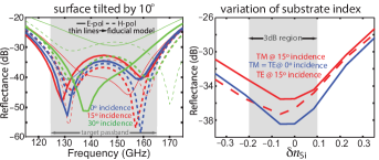
Application to tilted surfaces:
The left panel of Figure 14, left compares the performance of this coating applied to a surface tilted by compared with the performance when applied to a flat surface. Fortuitously, this effect improves performance at large angles of incidence and has little effect at small angles. Applying this coating by making grooves parallel to the lens symmetry axis of a curved lens will produce acceptable performance.
Groups of broken posts:
Assessing the impact of the broken posts is not straight forward because the region and extent of illumination varies between the three lenses. The degradation due to broken posts would thus be a function of the effective aperture area of the lenses and the location of the defects in addition to the total area affected. Accurately quantifying this is beyond the scope of this work. Qualitatively, the degradation would be negligible if the fraction of total area affected is small and more importantly, the length scale of the individual affected areas is smaller than the wavelength of incident light. Simulating the impact of broken posts is computationally difficult. Therefore we resorted to a simplified model consisting of a unit-cell containing seven posts in a row with one broken off completely. This is equivalent to having one seventh of the posts destroyed. This pessimistic case produces band averaged reflections below 2% which is acceptable though it does produce non-trivial cross-polarization. We used simulation to estimate that keeping the number of broken posts below 1/700 would result in a negligible degradation in the overall performance of the coating.
| machining error | parameter | sensitivity | tolerance |
|---|---|---|---|
| m | (units of ) | ||
| pitch () | |||
| centering | see text | ||
| kerf | |||
| sloped walls | |||
| depth | |||
| asymmetric depth | |||
| tilted surface | see text | ||
| damaged row | NA | ||
| index | NA |
Index:
Figure 14, right shows the band averaged reflectance as a function of variation in the index. A conservative tolerance for the index is (). This leads to increases in the reflectance of less than 3 dB over the fiducial design. This tolerance is weaker than that imposed by the optical design.
The 3dB sensitivies derived in this section are summarized in Table 3. The band averaged reflectivity of the fiducial design is -31 dB at incidence which is significantly better than the requirements for the system.