Anomalous Hall effect in two-phase semiconductor structures: the crucial role of ferromagnetic inclusions
Abstract
The Hall effect in InMnAs layers with MnAs inclusions of - nm in size is studied both theoretically and experimentally. We find that the anomalous Hall effect can be explained by the Lorentz force caused by the magnetic field of ferromagnetic inclusions and by an inhomogeneous distribution of the current density in the layer. The hysteretic dependence of the average magnetization of ferromagnetic inclusions on an external magnetic field results in a hysteretic dependence of . Thus we show the possibility of a hysteretic dependence (i.e. observation of the anomalous Hall effect) in thin conductive layers with ferromagnetic inclusions in the absence of carriers spin polarization.
pacs:
61.72.uj, 72.20.My, 75.50.PpThe investigation of the anomalous Hall effect (AHE) is a widely used experimental method for the diagnostics of the magnetic and transport properties of ferromagnetic layers, in particular, those of diluted magnetic semiconductors (DMS) Hsu . In the conventional interpretation, the AHE is a consequence of an asymmetric scattering of spin-polarized charge carriers in ferromagnetic materials Nag . Thus the observation of the AHE is traditionally considered to be a proof of the presence of spin-polarized carriers. The spin polarization of carriers in DMS is usually attributed to a mechanism of indirect exchange interaction between transition metal ions via charge carriers Dietl ; Mac . In the high temperature region this mechanism should become slack Dietl ; Mac . However, the AHE was observed at room temperature or above in some Mn-doped semiconductors Chen ; Par ; Jia . The AHE was also observed at about 300 K in Co-doped TiO2 Shin ; Lee and (La,Sr)TiO3 Zhang layers containing Co clusters. In Refs. Shin ; Lee ; Zhang the appearance of AHE was related to spin polarization by extrinsic (induced by the clusters) spin orbit scattering. Earlier, it was also observed that in InMnAs layers obtained by laser deposition in gas atmosphere a clear hysteresis in the magnetic field dependencies of the Hall resistance manifests itself up to room temperature Dan .
In III-Mn-V layers the second-phase inclusions may appear during technology processes. In particular, nanosize ferromagnetic MnAs particles can be embedded in a semiconductor matrix Boe ; Well . The temperature dependences of the ferromagnetic resonance Dan and magnetization Dan2 for the InMnAs layers grown by laser deposition show a Curie temperature of about 330 K that is close to the Curie temperature for MnAs. It was shown in Ref. Dan that an increase of the Mn content, characterized by the technological parameter =, where and are the ablation times of the Mn and InAs targets, leads to a reinforcement of the hysteretic character of the dependences.
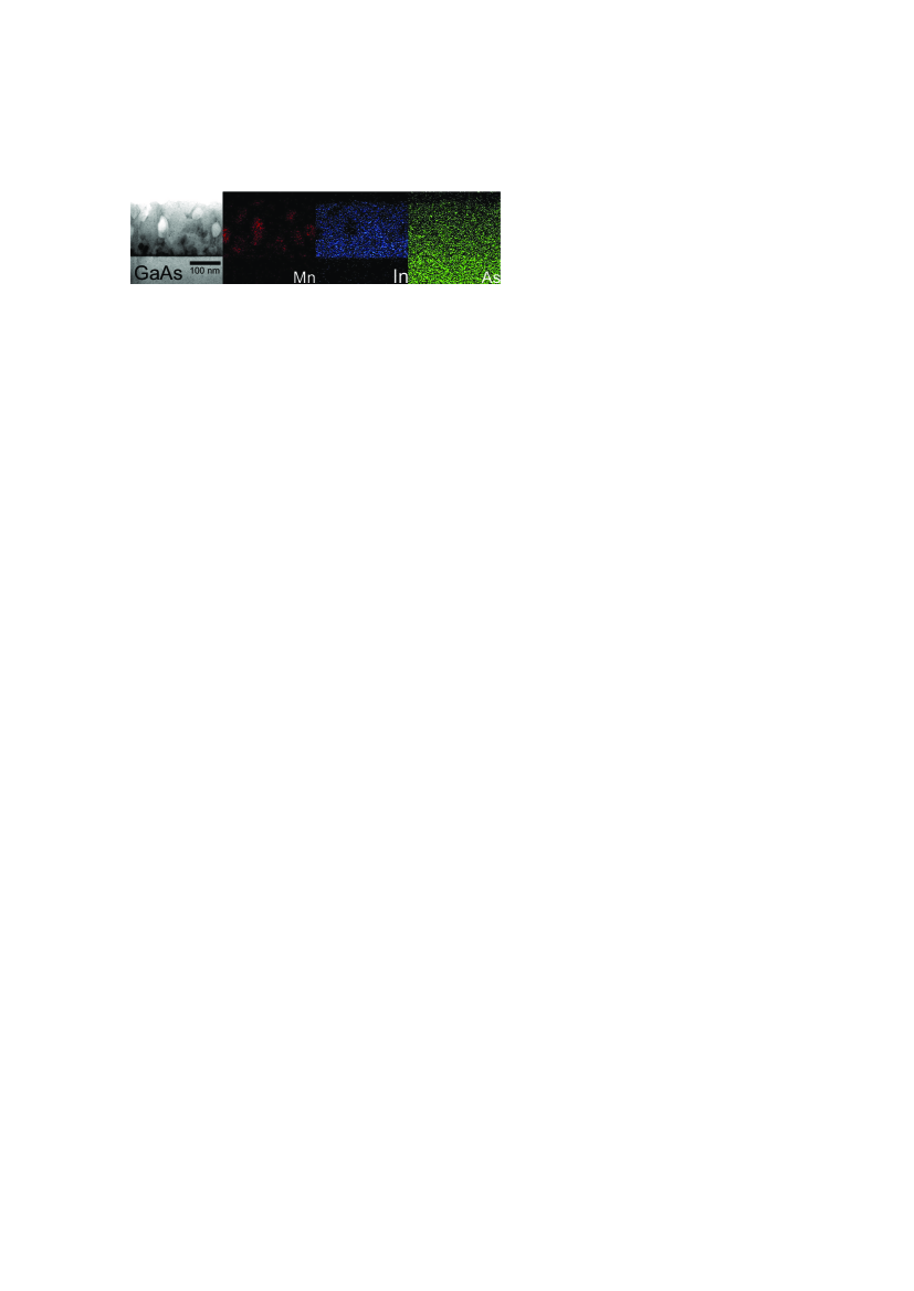
In this Letter, we present the results of theoretical and experimental investigations of the AHE in the InMnAs layers obtained by laser deposition. Nevertheless our results can be generalized to other conductive layers with ferromagnetic inclusions. Figure 1 shows the bright-field cross-sectional scanning transmission electron microscopy (STEM) image of the InMnAs/GaAs structure with =0.2. The image reveals a phase inhomogeneity of the InMnAs layer. Figure 1 also shows the energy-dispersive X-ray spectroscopy (EDS) mapping of Mn, In and As in the structure. The bright areas in the Mn mapping image correspond to the regions of predominantly Mn atoms. At the same time these regions are free from In atoms. Taking into account the uniform distribution of As atoms it can be concluded that the bright areas at Mn mapping image correspond to the inclusions of a MnAs phase. Thus the InMnAs layers contain MnAs clusters of 20-50 nm size.
Let us assume that the semiconductor matrix has no magnetic ordering at the temperatures considered (200-300 K) and the charge carriers have no predominant spin polarization. This assumption is based on the theory of carrier-mediated ferromagnetism which demands much higher carrier concentrations for the appearance of a ferromagnetic ordering in DMS than those found in our InMnAs layers ( cm-3 as will be shown below). In this case the magnetic properties of this structure are determined only by the ensemble of ferromagnetic MnAs inclusions. We also neglect the possible presence of any spin-dependent processes, even if the magnetic nanoparticles participate in the transport of electric charges.
The Lorentz force arises from the interaction of the magnetic fields of the ferromagnetic nanoparticles and the movements of the charge carriers. Moreover, an inhomogeneous distribution of the current density should be observed due to the layer heterogeneity. The principal idea of this Letter is to show that such a simple model is sufficient to describe qualitatively and quantitatively the hysteretic dependences of the Hall resistance on an external magnetic field in a conductive non-magnetic matrix containing ferromagnetic inclusions, without taking into consideration any spin-related phenomena.
The magnetic properties of an ensemble of ferromagnetic particles are dependent mainly on the magnetic anisotropy of the particle and the particle volume . These parameters define a blocking temperature of the ensemble which separates the superparamagnetic state from the blocked one according to the relationship Neel , where is the Boltzmann constant. As is known Blois , MnAs has an ”easy-plane” magnetocrystalline anisotropy for which should be 0 K. Thus it cannot provide the blocked character of the magnetization reversal with the coercivity kOe, as it was observed for our InMnAs layers Dan ; Dan2 as well as for 20-100 nm size MnAs clusters embedded in a GaAs matrix Boe ; Well . At the same time, the particles have an elongated shape (see Fig. 1) and in our case it is apparently the main source of the magnetic hysteresis. The microscopy revealed that the typical particle shape is an ellipsoid with the axes . This results in the effective uniaxial anisotropy constant erg/cm3 for 600 emu/cm3 (Ref. Blois ). So, to be unblocked at room temperature, the particle size must be less than 15 nm. The observed particles are several times larger than this (Fig. 1). Therefore the considered ensemble of the MnAs nanoparticles is in the blocked state at room temperature and thus possesses a coercivity.
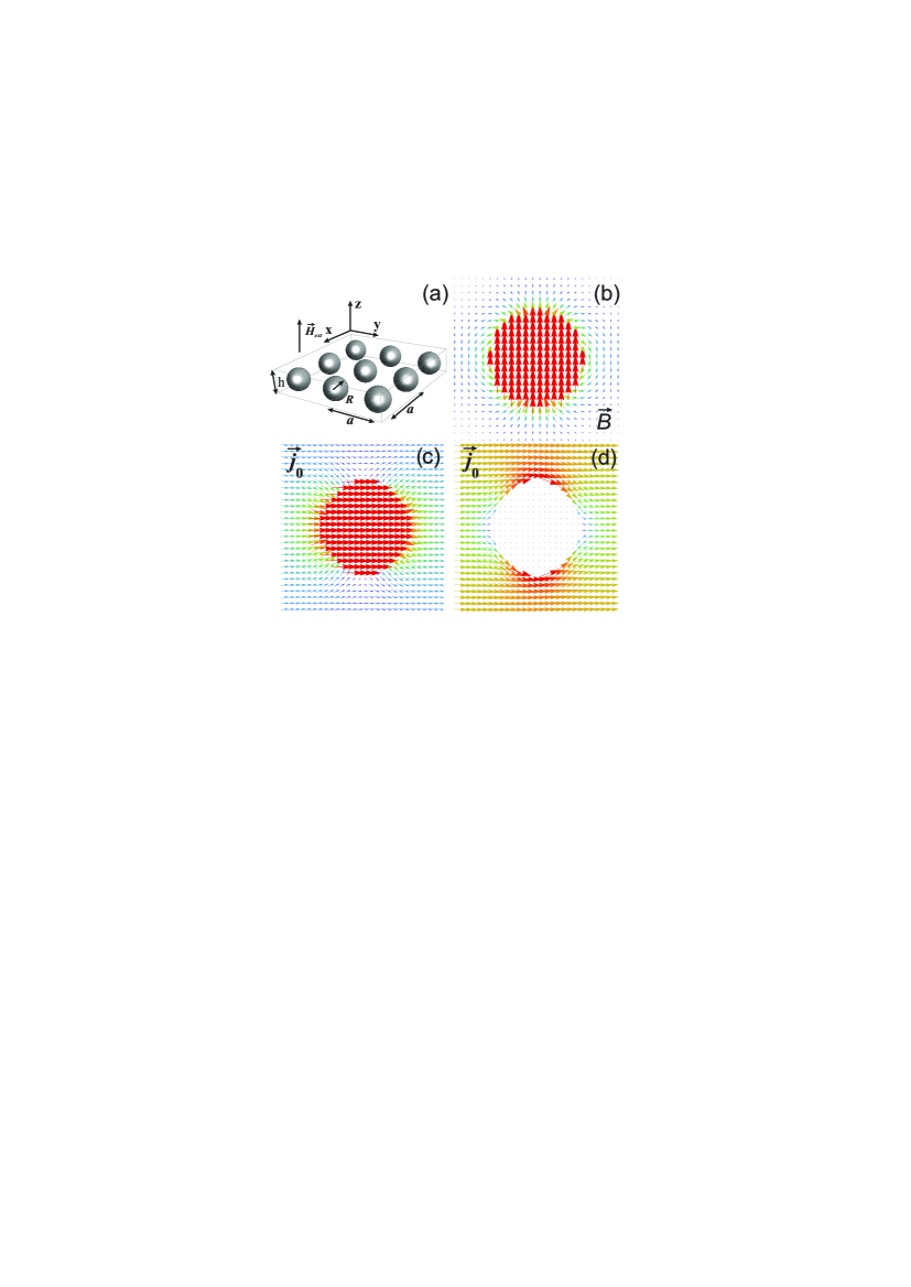
In the direction (normal to the layer plane), the film contains one or a few MnAs particles (Fig. 1). Thus a two-dimensional lattice of spherical ferromagnetic particles can be taken as the simplest model of the considered system (Fig. 2(a)). If the system is classically described and there is no barrier for carriers at the particle/matrix interface then the semi-metallic MnAs particles in a semiconductor matrix can be considered as a region with enhanced conductivity. We assume that a current flows in the direction then the current density outside the particle is
| (1) |
while the current density inside the particle is
| (2) |
where denotes the current density far from a particle. The origin of coordinates is in the center of a particle. The conductivity of the semiconductor matrix is characterized by a value and the conductivity of the particle is . Since , the current lines are involved into the particle as shown in Fig. 2(c) and the current density in the particle is distinctly higher than far from it. On the other hand the particle/matrix interface can be a barrier for carriers. Consequently the particle can be considered as a region with low effective conductivity () and the current flow will bend around the inclusion (Fig. 2(d)). In the limiting case when the barrier is impenetrable, charge carriers move in a space between the inclusions in a magnetic field produced by the inclusions and in an external magnetic field. It will be shown hereafter that, regardless of whether there is a barrier or it is absent, the hysteretic dependence of the Hall resistance on an external magnetic field () will be observed. This is attributed to the system heterogeneity and to the hysteretic dependence of the inclusion magnetization on an external magnetic field.
For the layer in the external magnetic field applied along the direction the average force acting on carriers per unit volume is defined as
| (3) |
where is the volume of the layer per ferromagnetic particle. Assuming that all the particles are uniformly magnetized along the direction each particle produces the magnetic field at the point equal to
| (4) |
where is the magnetic moment of the particle, is the magnetization of the latter. The particle with the number is subject to the external magnetic field and the fields of the other particles (4). Assuming that the distance between the particles noticeably exceeds the field produced by all other particles near the -th particle can be considered as locally homogeneous , where is the volume fraction of the ferromagnetic inclusions. Consequently, the field inside each particle is
| (5) |
The field in the space between the particles cannot be considered as homogeneous, but hereinafter we will use only the average value of the field. Since the volume per particle is and all the particles are identical, we find the average field in the space between the particles using the superposition principle
| (6) |
where integration is over the layer volume. The substitution of Eq. (4) into Eq. (6) yields
| (7) |
and owing to the problem symmetry.
Let us examine two limit cases. (i) Let a barrier for carriers at the particle/matrix interface be present, so . In this case as it follows from Eq. (2) and the current flow does not penetrate into the inclusion. Therefore the charge carriers move in the space between the inclusions in the average field Eq. (6). (ii) If the barrier is absent then . Hence the current density in the particle is (Eq. (2)) and the current flow is involved into the particle. In this case carriers inside the particle are subject to the magnetic field Eq. (5). For the case (i) the average Lorentz force can be approximately found in according to Eqs. (3), (7) as
| (8) |
and for the case (ii) according to Eqs. (3), (5), (7) as
| (9) |
where is the particle volume and . According to Eqs. (8) and (Anomalous Hall effect in two-phase semiconductor structures: the crucial role of ferromagnetic inclusions), the average Lorentz force depends on the magnetization of the particles. It should be noted that for the case (i) the sign of the first term in Eq. (8) is different from that for the case (ii) Eq. (Anomalous Hall effect in two-phase semiconductor structures: the crucial role of ferromagnetic inclusions). This will be discussed in more detail hereafter. The MnAs inclusions are ferromagnetic and the hysteretic dependence of the magnetization on the external magnetic field leads to a hysteretic dependence of the Hall resistivity on the external magnetic field , where is the charge carrier concentration in the semiconductor matrix, and is the electron charge. According to Eqs. (8) and (Anomalous Hall effect in two-phase semiconductor structures: the crucial role of ferromagnetic inclusions) the remanent Hall resistance is
| (10) |
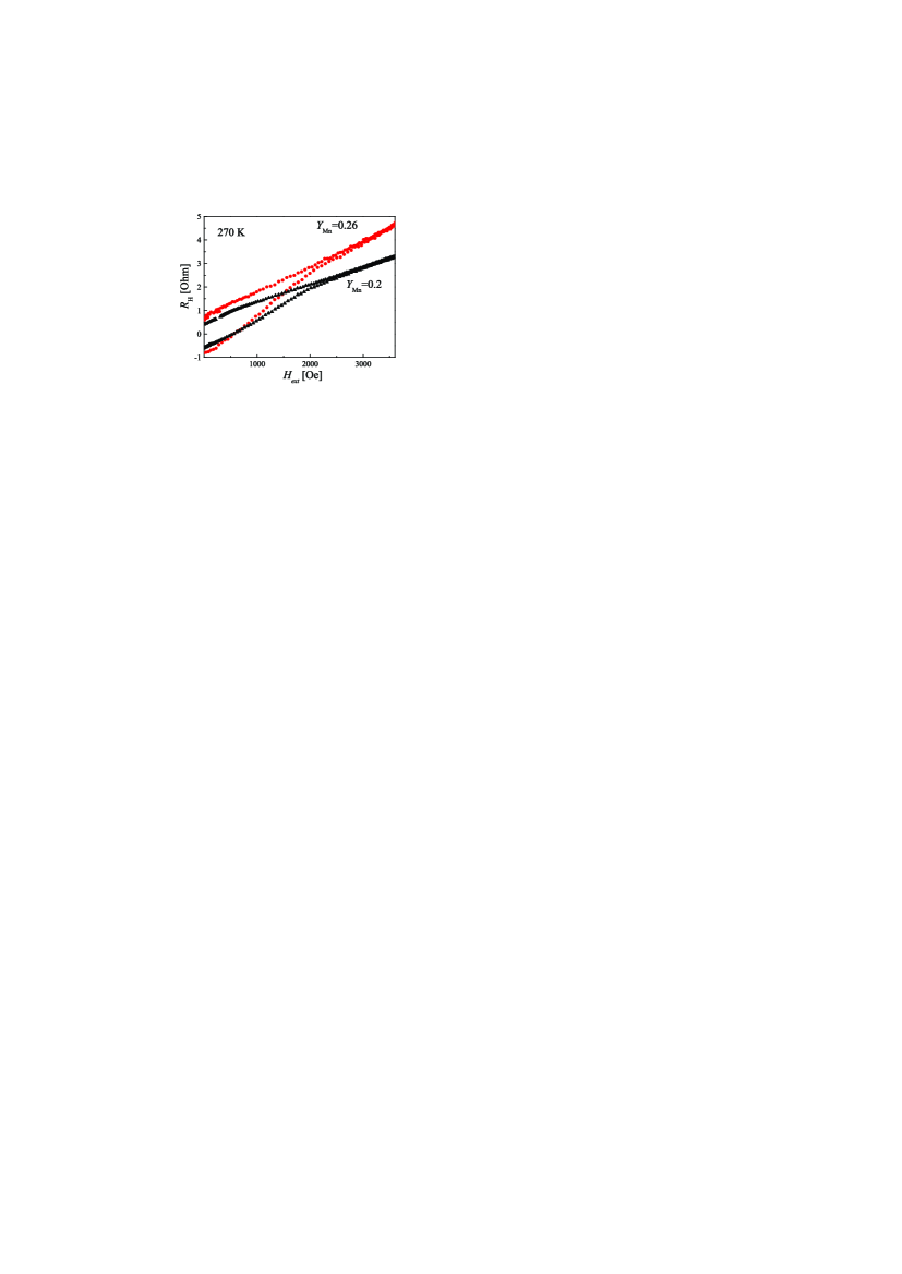
where for and for . As an estimation of we take the value of the remanent magnetization of an epitaxial MnAs layer (about 900 G at 270 K Xu ). The typical value of the carrier concentration for our InMnAs layers at 270 K is about cm-3 and the layer thickness 190 nm. For the volume fraction of the MnAs inclusions in the InMnAs layer is about 0.05 (Fig. 1), the value of equals approximately 0.5 Ohm, which is in a good agreement with the experimental results (Fig. 3).
Since for the discussed model the hysteresis in the dependence is due to the Lorentz force, it can be attributed to the ordinary Hall effect (OHE). Consequently, for a fixed volume fraction and a magnetization value of the MnAs particles in the layer, the value of the remanent Hall resistance should increase with decreasing the carrier concentration, in accordance with Eq. (10).
| Fluence (cm-2) | Carrier concentration | Carrier concentration |
|---|---|---|
| at 300 K (cm-3) | at 200 K (cm-3) | |
| 0 | () | () |
| () | () | |
| () | () | |
| () | () | |
| () | () | |
| () | () |
It is known that the ion irradiation can vary the carrier concentration of in semiconductors due to the formation of radiation-induced crystal defects. A feature of the InAs semiconductor is that radiation defects shift the Fermi level toward the conduction band, which leads to an increase of the carrier concentration in the n-type material or the p-n type conversion in p-InAs (Ref. Brud ). To change the carrier concentration in the InMnAs layer, the proton implantation was carried out with an energy of 50 keV and a fluence in the range - cm-2. Table 1 shows the values of the carrier concentration at 300 and 200 K in the InMnAs layer with =0.2 before and after irradiations with different proton fluences. The values of the carrier concentration were determined from the slope of the dependences in above 3000 Oe, i.e. mainly in the linear region. The temperature of 200 K was the lowest one at which it was possible to obtain the dependences for a high resistance layer irradiated by protons with a fluence of cm-2.
Proton implantations with fluences of and cm-2 lead to a decrease in the concentration of carriers (holes) as a result of the partial compensation of the Mn acceptor impurity by radiation-induced donor-type defects (Table 1). The conversion of the conductivity type from p to n is observed after the implantation with a fluence of cm-2. With a further increase in the proton fluence to cm-2 the concentration of the majority carriers (electrons) rises (Table 1). We suppose that the proton implantation does not lead to a significant modification of the magnetic properties of the semi-metallic MnAs inclusions.
Figure 4 shows the dependences at 200 K for the InMnAs layer with different carrier concentration values. For a fixed the Hall resistance value of the linear part of the dependence increases with decreasing carrier concentration. This is typical of the OHE and is related to the increase of the Hall coefficient . We emphasize that both for the cases of the p- and n-type majority carriers the clear increase of the remanent Hall resistance with decreasing carrier concentration is also observed (Fig. 4). So, the experimental results are in a good agreement with our model: the value increases with decreasing carrier concentration.
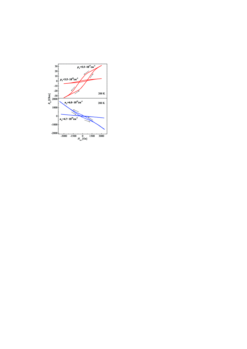
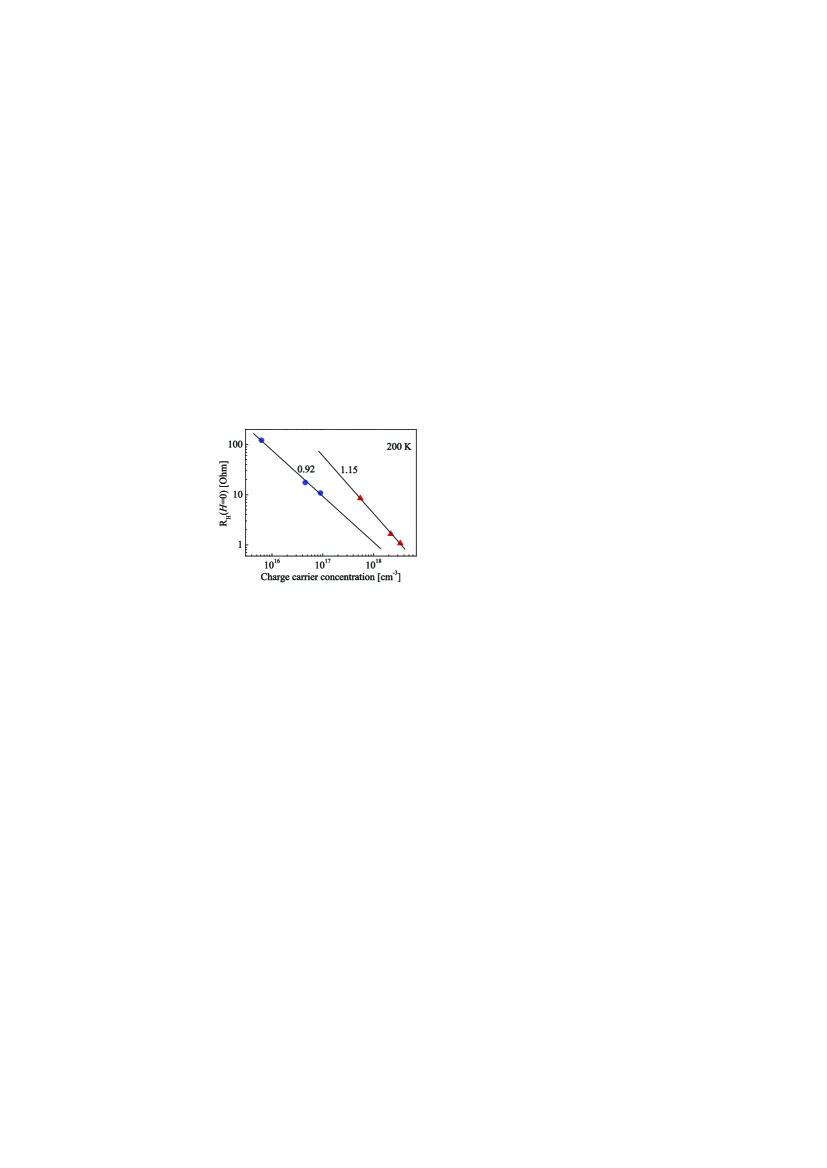
Figure 5 shows the experimental dependences of the remanent Hall resistance on the carrier concentration at a temperature of 200 K. Since for the OHE the Hall resistance is inversely proportional to the carrier concentration, the dependence of the remanent Hall resistance on the concentration in the double-logarithmic coordinates should be linear (Fig. 5). The linear approximation of the experimental points is shown in Fig. 5. The slope coefficients are sufficiently close to unity (as shown in Fig. 5) which corresponds to the assumption about the determinative role of the OHE (Eq. 10) in the observed hysteretic dependences Ber . We note that for a fixed carrier concentration the remanent Hall resistance will be higher for the p-type carriers than for the n-type carriers (Fig. 5). This effect has been predicted by the proposed model. It follows from Eqs. (8)– (10) that in the case when the conductivity of the inclusions is higher than that of the matrix, the influence of the magnetic field of the inclusions on the Hall effect will be two times higher than in the opposite case. Thus it is possible to conclude that for holes the barrier at the cluster/matrix interface is absent. However for electrons an impenetrable barrier at the cluster/matrix interface is present, which causes their predominant movement in the InMnAs layer between the MnAs clusters. It is known that MnAs is a p-type ferromagnetic semi-metal. This is in a good agreement with our conclusion about the presence of a barrier for electrons between the InMnAs matrix and the MnAs cluster.
It should be noted that, for p-type carriers, the sign of the linear component of the dependencies coincides with the sign of the hysteretic component. For n-type carriers these components have a different sign (Fig. 4). The difference between the signs of the linear component is related to the different type of carriers. At the same time, both for the p- and n-type majority carriers the sign of the hysteretic component is the same (Fig. 4). The reason for that is the following. The holes are affected by the Lorentz force. This leads to the average Lorentz force given by Eq. Anomalous Hall effect in two-phase semiconductor structures: the crucial role of ferromagnetic inclusions. Since the direction of the magnetization of the MnAs clusters (at the saturation point) coincides with that of (Fig. 2(b)) the sign of the hysteretic component of the dependence (which is determined by the magnetization of the MnAs inclusions) is equal to the sign of the linear component which is determined by . In contrast, in n-type layers the majority carriers (electrons) move between the MnAs inclusions in the magnetic field of inclusions and in the external magnetic field. However the magnetic field which is produced by the clusters has the opposite direction to the magnetization of the clusters (Fig. 2(b)) and is consequently opposite to . This leads to the difference in the signs of the terms in equation (8) for the average Lorentz force and to the difference in the signs of the linear and hysteretic components of the dependencies for n-type layers (Fig. 4).
Based on all the issues discussed above we can conclude that the apparent AHE in thin conductive layers with ferromagnetic inclusions can be related to the influence of local magnetic fields produced by the particles on charge carriers and an inhomogeneous distribution of the current density in the layer. Thus we have demonstrated the possibility of the pronounced anomalous Hall effect in the absence of the spin polarization of charge carriers.
The authors thank B.N. Zvonkov for the growth of the samples and V.K. Vasiliev for the proton implantation. We acknowledge support from RFBR (grants No. 12-07-00433-a, No. 12-07-31161), FCT through grants and projects PEst-C/CTM/LA0025/2011, RECI/FIS-NAN/0183/2012, SFRH/BPD/74086/2010 and by the European project Mold-Nanonet .
References
- (1) H.S. Hsu, C.P. Lin, S.J. Sun,H. Chou, Appl. Phys. Lett. 96, 242507 (2010).
- (2) N. Nagaosa, J. Sinova, S. Onoda, A.H. MacDonald, N.P. Ong, Rev. Mod. Phys. 82, 1539 (2010).
- (3) T. Dietl, H. Ohno, F. Matsukura, Phys. Rev. B 63, 195205 (2001).
- (4) A.H. Macdonald, P. Schiffer, N. Samarth, Nature Mater. 4, 195 (2005).
- (5) X. Chen, M. Na, M. Cheon, S. Wang, H. Luo, B.D. McCombe, X. Liu, Y. Sasaki, T. Wojtowicz, J. K. Furdyna, S.J. Potashnik, P. Schiffer, Appl. Phys. Lett. 81, 511 (2002).
- (6) N.D. Parashar, N. Rangaraju, V.K. Lazarov, S. Xie, B.W. Wessels, Phys. Rev. B 81, 115321 (2010).
- (7) J.-H. Yao, H.-H. Lin, Y.-L. Soo, T.-S. Wu, J.-L. Tsai, M.-D. Lan, T.-S. Chin, Appl. Phys. Lett. 100, 092404 (2012).
- (8) S.R. Shinde, S.B. Ogale, J.S. Higgins, H. Zheng, A.J. Millis, V.N. Kulkarni, R. Ramesh, R.L. Greene, T. Venkatesan, Phys. Rev. Lett. 92, 166601 (2004).
- (9) Y. J. Lee, M.P. de Jong, W.G. van der Wiel, Y. Kim, J.D. Brock, Appl. Phys. Lett. 97, 212506 (2010).
- (10) S.X. Zhang, W. Yu, S.B. Ogale, S.R. Shinde, D.C. Kundaliya, Wang-Kong Tse, S.Y. Young, J.S. Higgins, L.G. Salamanca-Riba, M. Herrera, L.F. Fu, N.D. Browning, R.L. Greene, T. Venkatesan, Phys. Rev. B 76, 085323 (2007).
- (11) Yu.A. Danilov, A.V. Kudrin, O.V. Vikhrova, B.N. Zvonkov, Yu.N. Drozdov, M.V. Sapozhnikov, S. Nicolodi, E.R. Zhiteytsev, N.M. Santos, M.C. Carmo, N.A. Sobolev, J.Phys. D: Appl. Phys. 42, 035006 (2009).
- (12) J. De Boeck, R. Oesterholt, A. Van Esch, H. Bender, C. Bruynseraede, C. Van Hoof, G. Borghs, Appl. Phys. Lett. 68, 2744 (1996).
- (13) P. J. Wellmann, J.M. Garcia, J.-L. Feng, P.M. Petroff, Appl. Phys. Lett. 71, 2532 (1997).
- (14) Danilov Yu., Drozdov Yu., Kudrin A., Vikhrova O., Zvonkov B., Sapozhnikov M., Fetisov L., Semisalova A., Perov N., J. Phys. D: Conf. Ser. 200, 062025 (2009).
- (15) L. Neel, Ann. Geophys. 5, 99 (1949).
- (16) R.W. De Blois, D.S. Rodbell, J. Appl. Phys. 34, 1101 (1963).
- (17) P. Xu, J. Lu, L. Chen, S. Yan, H. Meng, G. Pan, J. Zhao, Nano. Res. Lett. 6, 125 (2011).
- (18) V.N. Brudnyi, S.N. Grinyaev, N.G. Kolin, Physica B 348, 213 (2004).
- (19) J. J. Berry, S.J. Potashnik, S.H. Chun, K.C. Ku, P. Schiffer, N. Samarth, Phys. Rev. B 64, 052408 (2001).