Unusual reflection of electromagnetic radiation from a stack of graphene layers at oblique incidence
Abstract
We study the interaction of electromagnetic (EM) radiation with single-layer graphene and a stack of parallel graphene sheets at arbitrary angles of incidence. It is found that the behavior is qualitatively different for transverse magnetic (or polarized) and transverse electric (or polarized) waves. In particular, the absorbance of single-layer graphene attains minimum (maximum) for () polarization, at the angle of total internal reflection when the light comes from a medium with a higher dielectric constant. In the case of equal dielectric constants of the media above and beneath graphene, for grazing incidence graphene is almost 100% transparent to polarized waves and acts as a tunable mirror for the polarization. These effects are enhanced for the stack of graphene sheets, so the system can work as a broad band polarizer. It is shown further that a periodic stack of graphene layers has the properties of an one-dimensional photonic crystal, with gaps (or stop–bands) at certain frequencies. When an incident EM wave is reflected from this photonic crystal, the tunability of the graphene conductivity renders the possibility of controlling the gaps, and the structure can operate as a tunable spectral–selective mirror.
pacs:
81.05.ue,72.80.Vp,78.67.WjI Introduction
Electromagnetic (EM) metamaterial engineering yields specific optical properties which do not exist in natural materialsEngheta and Ziolkowski (2006). These properties include EM energy concentration in sub-wavelength regions and radiation guidingHan and Bozhevolnyi (2013), enhanced absorptionKravets et al. (2008), reflectionJoannopoulos et al. (2008) and transmissionGarcia de Abajo (2007), colour filteringXu et al. (2010), etc. An important and prominent example of metamaterials and their specific properties are photonic crystals (PCs)111Although photonic crystals are different from the ”classical” metamaterials (devices with negative refractive index) since the wavelength of operation is comparable to their structural period, the term ”metamaterial” nowadays is applied to any artificial structure with designed material (in our case, optical) properties., where the propagation of electromagnetic waves of certain frequencies, belonging to gaps (or stop-bands) in the spectrum, can be prohibited, or allowed in certain directions onlyJoannopoulos et al. (2008). Thus, the so called three-cylinder structureYablonovitch et al. (1991) was the first experimental realization of full photonic band gap, where the propagation of electromagnetic waves is not possible in any direction. The photonic band-gap structure of PC resembles and appears in full analogy with the electronic one in solid-state crystals.
In the metamaterial´s engineering it is useful to implement some tools for adjusting their EM properties, thus achieving the tunability. Tunable metamaterials allow for continuous variation of their properties through a certain external influence (for review see, e.g. Refs.Boardman et al. (2011); Vendik et al. (2012); Liu et al. (2012a)). Among the possible instruments to achieve the PC´s dynamical tunability we can mention the optical beam intensity in a nonlinear material Chen et al. (2011), electric field in ferroelectricsFigotin et al. (1998), applied voltage in liquid crystalsOzaki et al. (2002); Li (2007), magnetic field in ferromagnets or ferrimagnets Figotin et al. (1998); Kee et al. (2000), and mechanical force for changing the PC periodPark and Lee (2004). There are also possible tuning mechanisms in crystalline colloidal arrays of high refractive index particles Han et al. (2012), magnetic fluidsZu et al. (2012) or superconductors Savel’ev et al. (2005, 2006).
The two-dimensional carbon material graphene possesses a number of unique and extraordinary properties, such as high charge carrier mobility, electronic energy spectrum without a gap between the conduction and valence bands, and frequency-independent absorption of EM radiation. The optical properties of graphene have been extensively studied both theoretically Peres et al. (2006); Falkovsky and Pershoguba (2007); Stauber et al. (2007); Stauber et al. (2008a, b); Gusynin et al. (2009); Grushin et al. (2009); Mishchenko (2009); Castro Neto et al. (2009); Peres (2010); Yang et al. (2009); Peres et al. (2010); Ferreira et al. (2011); Liu et al. (2012b) and experimentally Nair et al. (2008); Kuzmenko et al. (2008); Mak et al. (2008); Wang et al. (2008); Kuzmenko et al. (2009); Crassee et al. (2011); Bao et al. (2011); Li et al. (2008). Since the carrier concentration in graphene (and, hence, its frequency–dependent conductivity) can be effectively tuned in wide limits by applying an external gate voltage Li et al. (2008), it is a perspective material for tunable photonic components. For example, in the area of plasmonics it is possible to make devices such as tunable graphene-based switchBludov et al. (2010), polarizerBludov et al. (2012a), and polaritonic crystalBludov et al. (2012b). Moreover, using twoHwang and Das Sarma (2009); Svintsov et al. (2013); Stauber and Gómez-Santos (2012); Bludov et al. (2013) or moreEberlein et al. (2008); Jovanović et al. (2011); Hajian et al. (2013); Lee et al. (2011); Sreekanth et al. (2012); Iorsh et al. (2013) parallel sheets of graphene can result in an unusual optical response of the structure owing to the interaction of charge carriers in the different layers by means of EM waves. Alternatively, for the same purposes it is possible to use an array of graphene ribbonsJu et al. (2011); Nikitin et al. (2012a); Hipolito et al. (2012), two-Yan et al. (2012a); Thongrattanasiri et al. (2012) or three-dimensionalBerman et al. (2010); Yan et al. (2012b) arrays of graphene disks, or a two-dimensional array of antidotsNikitin et al. (2012b).
The aim of the present work is twofold. On the one hand, in the studies considering the transmittance of radiation through grapheneYang et al. (2009); Ferreira et al. (2011); Nair et al. (2008); Crassee et al. (2011) several authors analyzed only the case of normal incidence of the radiation on the graphene sheet. By restraining themselves to this particular case, these studies overlooked the unusual reflection and transmission properties taking place at oblique incidence. In this paper we discuss the transmission of EM radiation through a graphene sheet when the impinging beam makes an arbitrary angle, , with the normal to the interface. We will show that, at grazing incidence (i.e. for close to ) and when the graphene layer is cladded by two identical dielectrics, it behaves like a mirror for -polarized waves and is almost transparent for -polarized waves. (In contrast, if the dielectric constants of the media below and above the graphene sheet are different, the interface reflects almost totally both - and -polarised waves as it is usual at grazing incidence). Furthermore, for close to the total internal reflection angle, a single sheet of monolayer graphene strongly absorbs -polarized waves, while there is almost no -polarized absorption in these conditions. On the other hand, we theoretically investigate the reflection of EM radiation, in the THz to far-infrared (FIR) range and for arbitrary , from a periodic stack of parallel graphene sheets which constitute a semi-infinite one-dimensional (1D) photonic crystal. As it will be shown, this PC is highly reflective within certain frequency intervals corresponding to the gaps in its spectrum, and the widths of these gaps can be tuned by varying the gate voltage giving the possibility to create a tunable mirror. Moreover, when the angle of incidence for a -polarized wave exceeds that of total internal reflection, it is possible to excite a surface EM mode supported by the semi-infinite photonic crystal.
II Single-layer graphene
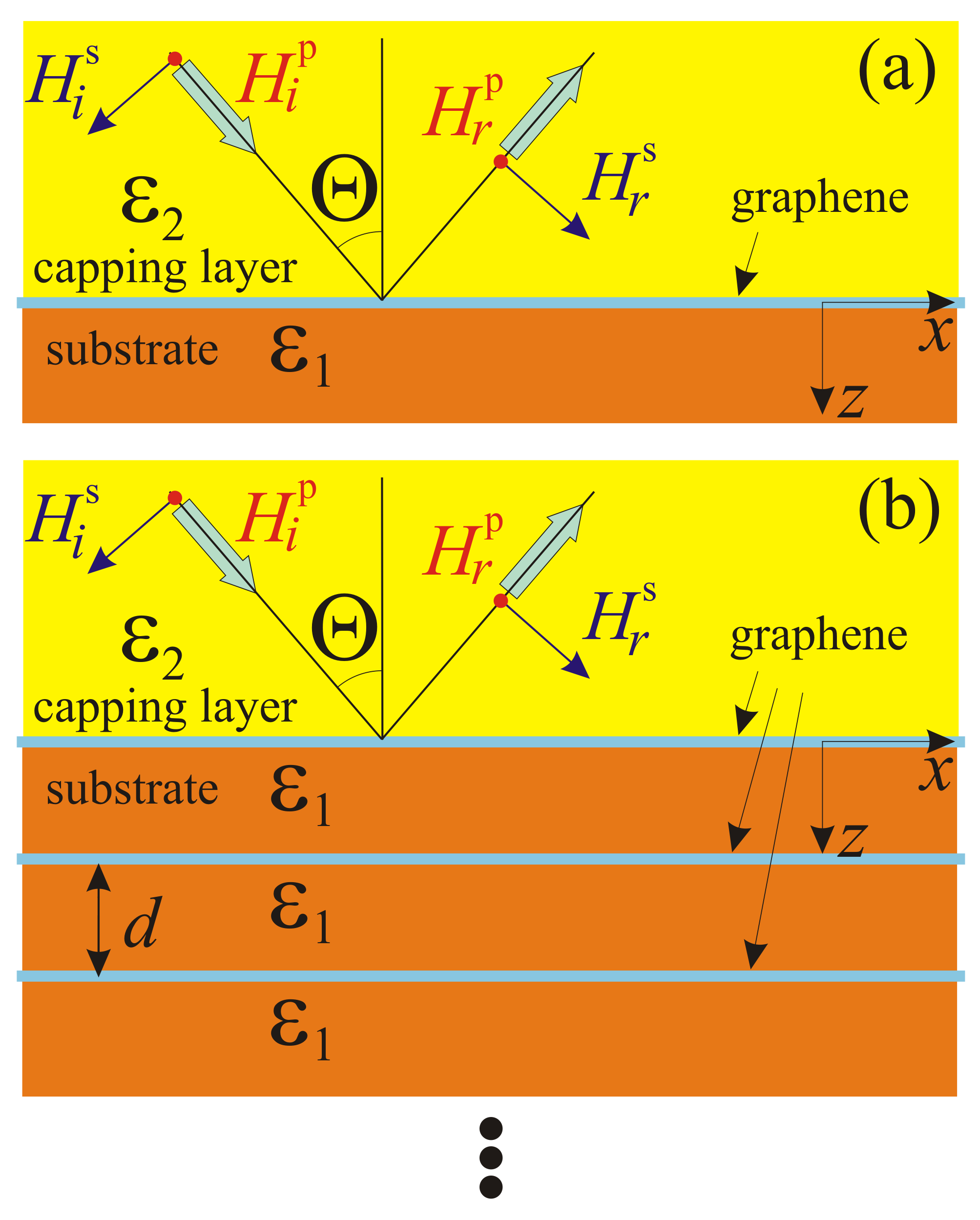
Let us first consider a single flat sheet of monolayer graphene located at the plane (so, the axis is perpendicular to it) and cladded by two semi-infinite dielectrics, a substrate with a dielectric permittivity and a capping medium with , occupying the half-spaces and , respectively [see Fig. 1(a)]. If the EM field is uniform along the direction (), it can be decomposed into two separate waves with different polarizations. Thus, a -polarized (or TM) wave with the magnetic field perpendicular to the plane of incidence (), possesses the electromagnetic field components , while an -polarized (or TE) wave is described by electromagnetic field components , with the electric field perpendicular to the plane of incidence.
The temporal dependence of the fields is assumed of the form, , where is the angular frequency of the radiation and the superscripts correspond to the electromagnetic field in the substrate and the capping dielectric, respectively. Maxwell equations written explicitly for TE and TM waves in this particular situation can be found in several previous publicationsBludov et al. (2010, 2012a, 2012b, 2013). We reckon that the EM wave falls on the interface from the capping dielectric side. In this case the solution of the Maxwell equations for a -polarized wave can be written as follows:
| (1) | |||
| (2) | |||
| (3) | |||
| (4) |
where
| (5) |
, is the velocity of light in vacuum.
At the same time, for an -polarized wave we have:
| (6) | |||
| (7) | |||
| (8) | |||
| (9) |
In Eqs. (1)–(4) and (6)–(9), , and denote the amplitudes of the incident, reflected and transmitted - ()-polarized waves, respectively.
In order to find the transmittance and the reflectance of the structure we apply boundary conditions at , which include the continuity of the tangential component of the electric field, ; , and the discontinuity of the tangential component of the magnetic field caused by the induced surface currents in graphene, , , where is the graphene conductivity. Matching the solutions for and using these boundary conditions, we obtain the amplitudes of the reflected and transmitted waves,
| (10) | |||
| (11) |
for -polarization and
| (12) | |||
| (13) |
for -polarization. The transmittance (reflectance) is expressed as the ratio of the Poynting vector -components of the transmitted (reflected) and the incident waves,
Since and are determined by the conductivity [see Eqs. (10)–(13)], we briefly consider its frequency dependence. The frequency–dependent (optical) conductivity of graphene is a sum of two contributions: (i) a Drude term describing intra-band processes, and (ii) a term taking into account inter-band transitions. At zero temperature the optical conductivity has a simple analytical expressionPeres et al. (2006); Falkovsky and Pershoguba (2007); Castro Neto et al. (2009); Peres (2010); Stauber et al. (2008b). The inter-band contribution has the form , where
| (14) |
and
| (15) |
where is the so called universal conductivity of graphene. The Drude conductivity term is
| (16) |
where is the inverse of the momentum relaxation time and is the Fermi level position with respect to the Dirac point. The total conductivity is
| (17) |
We can write , where is a dimensionless function. In Fig. 2 we depict the Drude and inter-band contributions to the total optical conductivity of graphene.
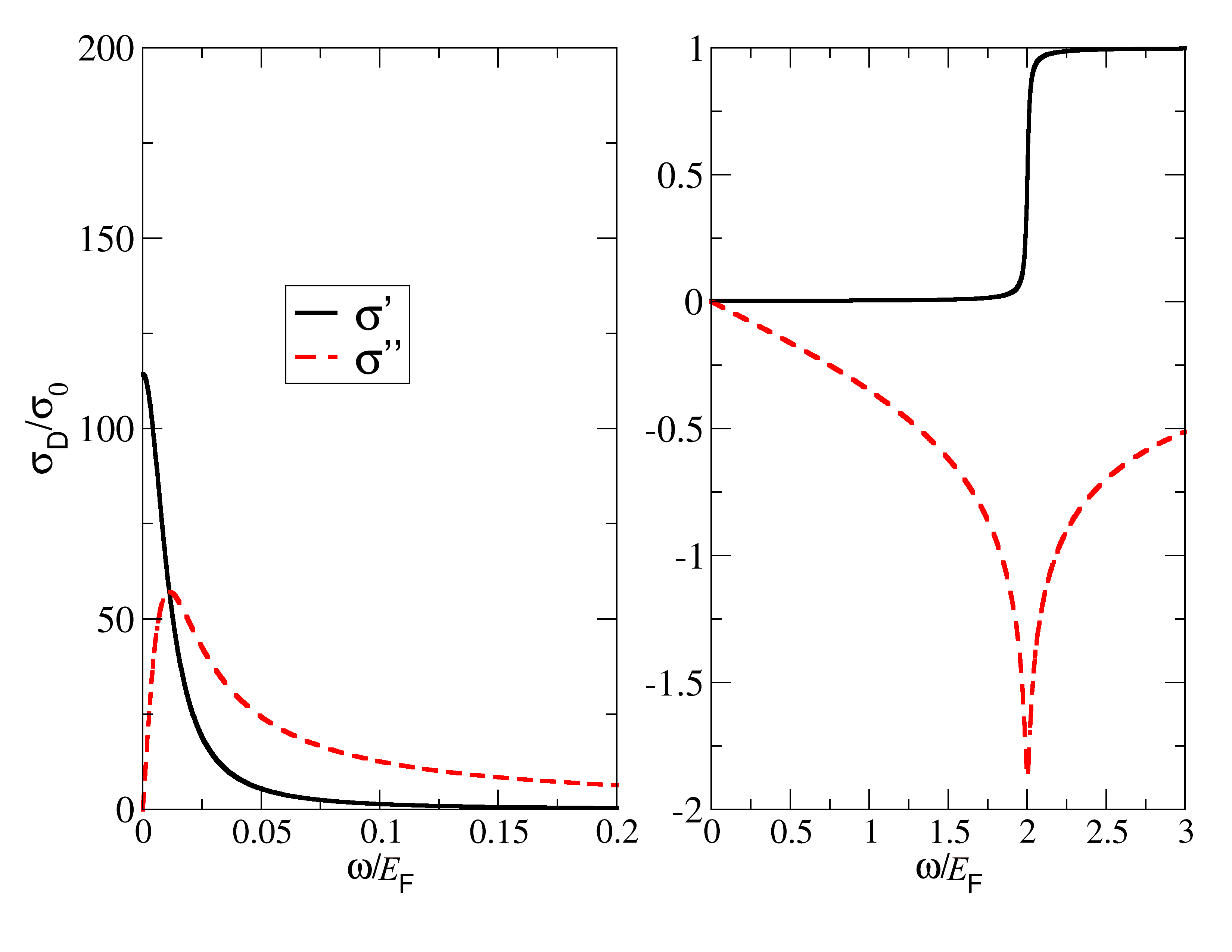
It is evident that at low-frequencies (left panel in Fig. 2) the Drude term significantly exceeds the interband one (both real and imaginary parts), while in the high-frequency range (right panel in Fig. 2) the interband term dominates. Moreover, in the vicinity of the threshold frequency, , the real part of the conductivity increases drastically and achieves the universal value, (onset of interband transitions), while the imaginary part is minimal, negative and of the order of several universal conductivities in modulus. As a result, at low frequencies the presence of graphene at the interface between two dielectrics influences significantly the reflectance and the transmittance of the structure. This effect, owing to the high value of the Drude conductivity, is clearly seen in Figs. 3 and 4(a–c), where the low-frequency region is characterized by the lower transmittance [see Figs. 3(a), 3(c), 3(e) and the respective insets for ], higher reflectance [Figs. 3(b), 3(d), 3(f) and the respective insets for ] and enhanced absorbance [Figs. 4(a)–4(c)] for all parameters’ values. In fact, the transmittance and the reflectance are mainly determined by the real part of the conductivity, except when the imaginary part is large in modulus (at low frequencies and near ).
At normal incidence (), we have (for any polarization):
| (18) | |||
| (19) |
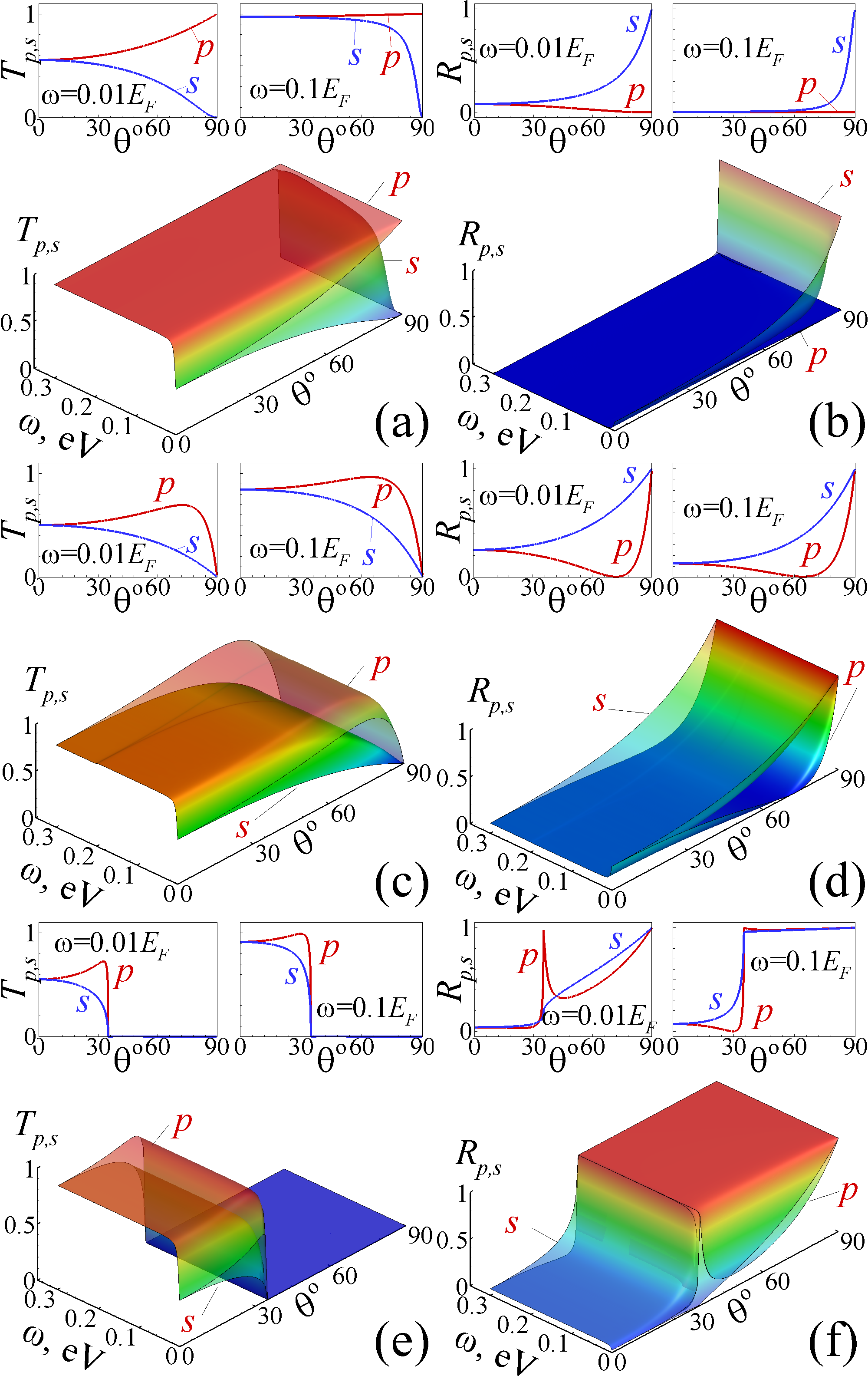
where is the fine structure constant. For oblique incidence (), the dependencies of the transmittance and the reflectance on are strongly affected by the relation between the dielectric permittivities of the substrate and the capping dielectric. Therefore, we considered all three possible situations: (i) [Figs. 3(a), 3(b)], (ii) [Figs. 3(c), 3(d)], and (iii) [Figs. 3(e), 3(f)]. In the ”symmetric” case of , the transmittance and the reflectance can be expressed by simple formulae,
| (20) | |||
| (21) | |||
| (22) | |||
| (23) |
Note that the factor multiplying the dimensionless function , which represents the frequency dependence of the graphene conductivity, is a small number (=0.023). Thus, unless the absolute value of is large, the term related to graphene in Eqs. (10)–(13) and, accordingly, in the above expressions for and is small. Therefore, the reflectance and the transmittance of the structure are close to the values defined by usual Fresnel’s expressions, except for and . In particular, the reflectance is proportional to .
It should also be noticed that in Eqs.(18), (19) and (20)–(23) the effect of graphene is stronger for lower dielectric constants and is maximal for free standing graphene (). As increases [see Figs. 3(a), 3(b) and the insets], the transmittance decreases and attains zero for , while the reflectance increases and tends to unity at . In contrast, a -polarized wave is ”totally transmitted” at (, ). With the electric field perpendicular to the graphene sheet (TM wave), no charge oscillations are induced at the interface and the EM field is not perturbed. Also, the low-frequency absorbance at grazing incidence is a decreasing function of the angle for both - and -polarized waves and the limit corresponds to zero absorbance [see Fig. 4(a)]. Note that the absorption is entirely related to graphene because the dielectrics are assumed dispersionless.
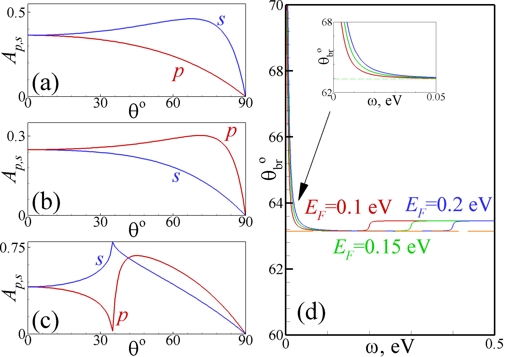
The situation is different when the dielectric constants of the substrate and capping dielectric are not equal because in this case there would be reflection even in the absence of graphene. Here, at grazing incidence the reflectance (transmittance) is close to unity(zero) for both polarizations [see Figs. 3(c)–3(f)], just like for a ”normal” interface between two dielectrics (without graphene). In the case (ii), although the angular dependence of the low-frequency absorbance [Fig. 4(b)] is qualitatively similar to the ”symmetric” case (i), it is higher for TM waves [cf. Fig. 4(b) and Fig. 4(a)], in contrast with the case (i). The particularity of the case (ii) (, e.g. uncovered graphene on a substrate) is that the angular dependence of the TM-wave reflectance [see Fig. 3(d)] possesses a minimum at a certain close to the Brewster angle for the two dielectrics considered, Born and Wolf (1980). Owing to the non-zero imaginary part of the graphene conductivity, the TM wave reflectance at this angle is finite, while it would reach zero in the case without graphene. Therefore we call this the “quasi-Brewster” angle, . It depends upon the frequency and the Fermi energy of graphene; this dependence is depicted in Fig. 4(d). At low frequencies, where the conductivity is high owing to the Drude term, the quasi-Brewster angle of the structure exceeds the conventional Brewster angle of the interface without graphene. This effect is more pronounced for higher values of the Fermi energy – compare the three curves in the plot. When the frequency grows (and the Drude term in becomes smaller) approaches the value of the conventional Brewster angle . However, at the quasi-Brewster angle jumps up because of the Fermi step in the real part of (onset of interband transitions). The difference between and the conventional Brewster angle, , characteristic of graphene–free interface between the same two dielectrics, can be used for visualization of graphene, which constitutes a considerable problem Goncalves et al. (2010). At low frequencies, can reach easily detectable values of .
In the last possible situation (iii), there is a critical angle of total internal reflection [ for the parameters of Figs. 3(e) and 3(f)]. Above this critical angle, , the transmittance vanishes and the reflectance is close to unity [see Figs. 3(e) and 3(f)]. Notice that the value of does not depend upon the graphene parameters. In the case under consideration, the low-frequency absorbance [Fig. 4(c)] exhibits the most interesting behavior: in the vicinity of the total internal reflection angle the absorbance of the polarized wave is almost zero, while that of the polarized wave reaches its maximum of .
III Graphene multilayer photonic crystal
Now we shall consider an external EM wave falling on the periodic multilayer structure [see Fig. 1(b)] consisting of an infinite number of parallel monolayer graphene sheets separated by dielectric slabs of thickness ; in practical terms few graphene layers play the same role as an infinite number of them Peres and Bludov (2013). The geometry of the problem is similar to considered in Sec.II, but with graphene layers (for which we shall assume the same Fermi energy) located at positions , . Thus, the considered structure is a semi-infinite 1D PC, terminated by the graphene layer at . We shall still consider a capping dielectric (with arbitrary real ) on top of it.
In order to find the reflectance of this PC, we notice, that the structure of the electromagnetic field in the capping dielectric is the same, as represented by Eqs. (1),(3) and (6),(8) for - and -polarized waves, respectively. At the same time, the fields in the substrate should be considered separately in each layer between adjacent graphene sheets at planes and . Namely, solutions of the Maxwell equations at spatial domain can be represented as
| (24) | |||
| (25) | |||
and
| (26) | |||
| (27) | |||
Here are the amplitudes for forward (sign ”+”) or backward (sign ”–”) propagating TM waves. Correspondingly, represent the amplitudes of the TE waves. The amplitudes can be related to by matching boundary conditions at on graphene (similar to that, used in Sec. II), namely:
| (32) | |||
| (35) |
Similarly, for polarization,
| (40) | |||
| (43) |
Since the considered structure is periodic 222The surface at , of course, breaks the translational symmetry. This symmetry breaking can give rise to local (surface) modes, known as Tamm states in the case of electronic structure of crystals (not to be confused with the Bloch-type TM surface wave discussed below!). However, the band structure of the spectrum is preserved and the surface EM mode can be excited only under special conditions, enhancing the in-plane wavevector Bludov et al. (2010, 2013)., it is possible to use the Bloch theorem, which determines the proportionality between the field amplitudes in the adjacent periods through the Bloch wavevector :
After substitution of these relations into Eqs.(32),(40), the compatibility condition of the resulting linear equations requires:
| (44) | |||
| (45) |
where is the unity matrix. Equations (44, 45) yield the dispersion relations for and polarized EM waves in the graphene multilayer PC:
| (46) |
and
| (47) |
We note that similar expressions have been obtained in Ref.Hajian et al. (2013)
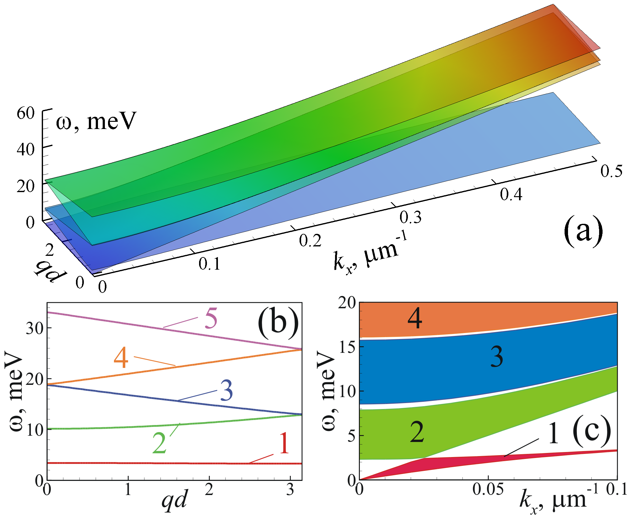
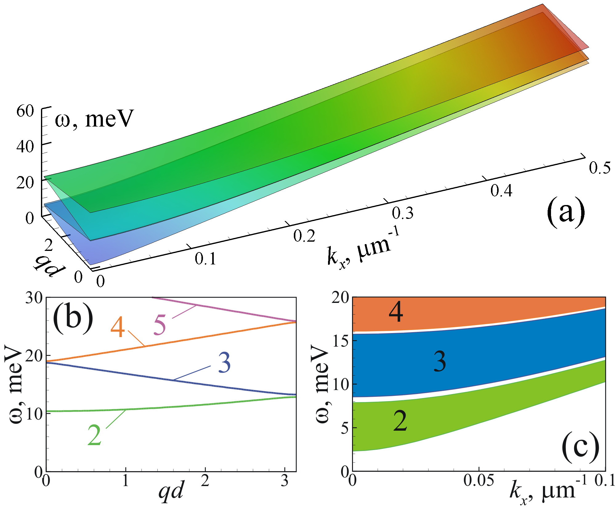
Before considering the dispersion properties of and polarized waves in detail, it should be noticed, that dispersion curves depicted in Figs. 5 and 6 have been calculated for zero damping, , when the graphene conductivity possesses only the imaginary part. As a result, the eigenfrequencies, the in-plane component of the wavevector , and the Bloch wavevector are real values. In the case of nonzero the eigenfrequencies will be complex values with imaginary part characterizing the mode damping. The calculated spectra exhibit the band structure of a photonic crystal for both (Fig. 5) and polarized waves (Fig. 6). In particular, there are gaps in the spectra [see Figs. 5(a) and 6(a)] that appear in the center () and in the edges () of the first Brillouin zone, and the widths of gaps decrease with the increase of [see Figs. 5(c) and 6(c)]. However, the main feature of the polarization spectrum is the presence of surface mode with purely imaginary [marked by 1 (red color) in Figs. 5(b) and 5(c)] together with bulk modes with purely real [marked by 2 (green), 3 (blue), 4 (orange) and 5 (pink) colors in Figs. 5(b) and 5(c)]. The former is a ”Bloch surface plasmon-polariton”, with the electric and magnetic fields strongly localized at the graphene sheets Bludov et al. (2013) but with a real Bloch wavevector. In the case of polarization such a surface mode does not exist and only bulk modes are present in the spectrum [see Figs. 6(b) and 6(c)].
Particular solutions of the dispersion relation for polarization, Eq. (46), for [so called ”Bragg modes”] can be represented as
| (48) |
For we have:
| (49) |
polarized Bragg modes [solutions of (47)] for are exactly the same as (48), but for they are similar to (49) (except that ). The modes with Bragg wavevectors, (48) and (49), have nodes at graphene layers and, therefore, these solutions do not involve the graphene conductivity, . As a matter of fact, these solutions correspond to for polarization and for polarization. It implies zero in-plane components of the electric field in both cases, consequently, no electric current is induced in graphene sheets located at [see Eqs. (25) and (26)].
Secondly, in the case of polarization is the solution that implies arbitrary and , and, as a result, independent upon as well as . At the same time, for polarization the solution corresponds to a trivial solution of the Maxwell equations with zero electric and magnetic fields. For polarization, the line is crossed by another dispersion curve at the point [see Fig. 5(c)], where there is no gap between the surface and bulk mode bands. Below this point, the solution corresponds to the top of the surface mode band, while above this it corresponds to the bottom of the bulk mode band. Similarly, the upper bands depicted in Figs. 5(c) and Fig. 6(c) are delimited by the Bragg modes, (48) and (49).
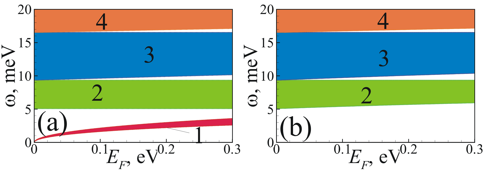
At the same time, changing the graphene Fermi energy, , e.g. by varying an external gate voltage, it is possible to tune the width of the gaps, as it can be seen from Figs. 7(a) and 7(b) (for and polarizations, respectively). In particular, the gaps vanish when the Fermi level coincides with the Dirac point. At the same time, the waveguide modes defined by Eqs. (48) and (49) remain unchanged because of their above-mentioned independence upon the graphene conductivity.
In order to obtain the expression for the reflectance of an EM wave from the graphene multilayer stack, we notice that, by virtue of Eqs. (44) and (47), the amplitudes and are related by:
where
| (50) | |||
| (51) |
and Bloch wavevector for and is obtained from Eqs.(46) and (47), respectively. It should be pointed out that, if the graphene conductivity is complex, so is the Bloch wavevector in Eqs. (50) and (51). Then, applying the above-mentioned boundary conditions at , one can obtain expressions for the amplitude of the reflected wave in the form:
| (52) | |||
| (53) |
Notice that, when , Eq. (52) coincides with Eq. (10) for the single graphene layer structure. Similarly, when , Eq. (53) turns into Eq. (12).
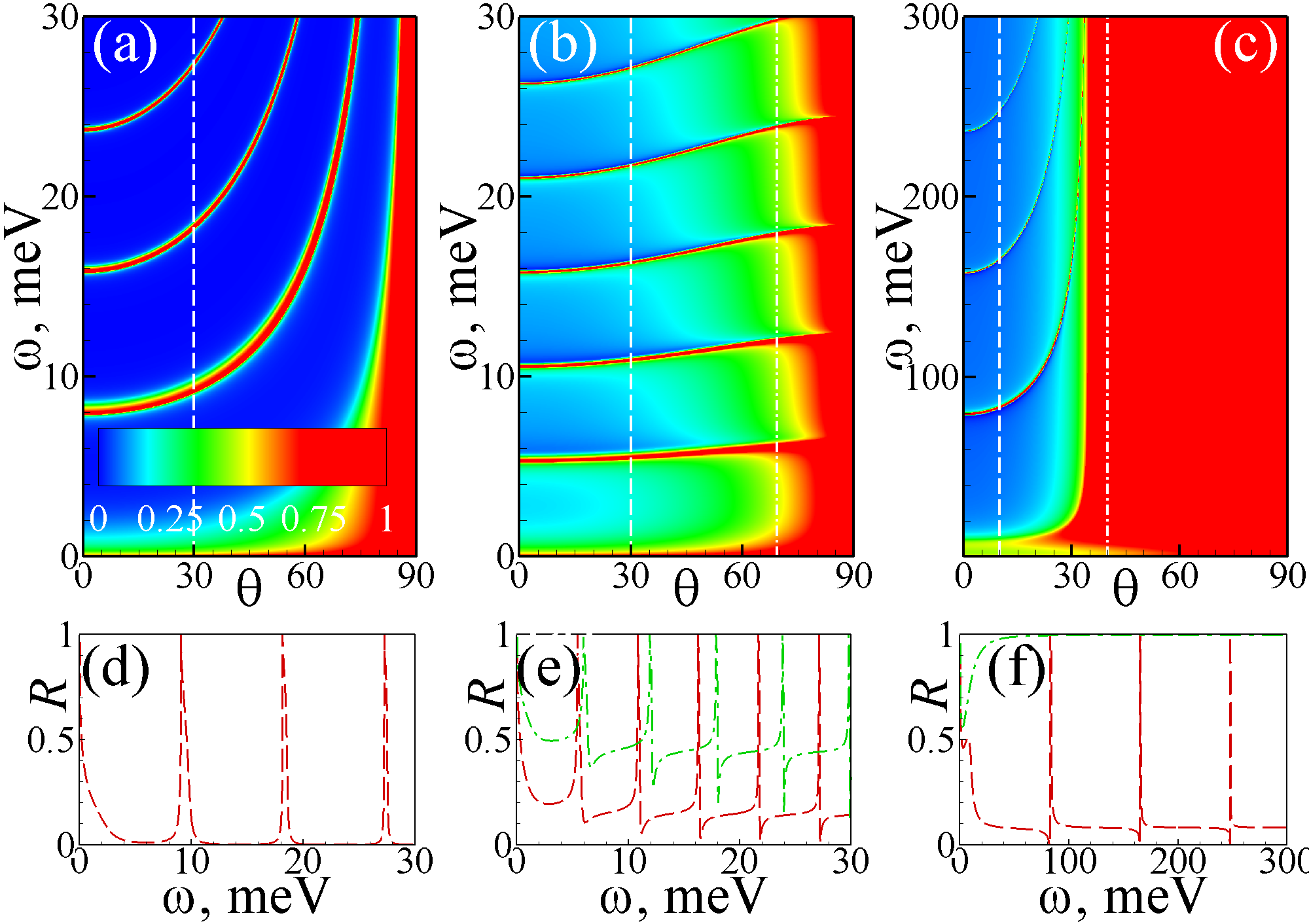
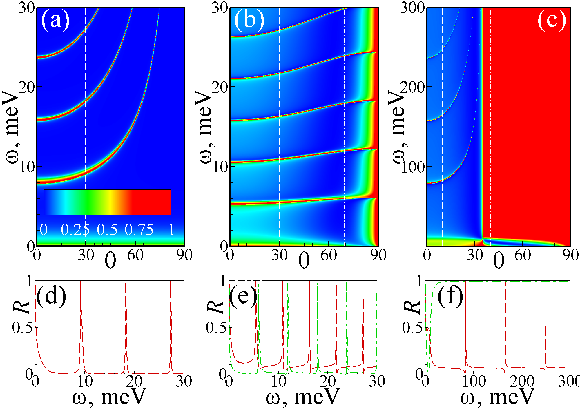
An incident wave with and inside one of the allowed bands of the photonic crystal is (partially) transmitted into the structure. This effect is clearly seen in Figs. 8 and 9 for and polarized waves, respectively). Thus, when and of the incident wave match one of the bands, the reflectance of the graphene multilayer photonic crystal resembles that of the single-layer graphene [compare Figs. 8(a), 9(a) with 3(b), as well as Figs. 8(b), 9(b) with 3(d) and Figs. 8(c), 9(c) with 3(f)].
On the contrary, incident EM waves with and belonging to the gaps of the PC band structure induce evanescent waves (characterized by imaginary Bloch wavevector , in contrast with the PC surface mode with real and imaginary ), and are nearly totally reflected from it. The graphene-multilayer PC reflectance is considerably higher than that of single-layer graphene heterostructure, and at certain frequencies can achieve unity [see panels (d),(e) and (f) in Figs. 8 and 9].
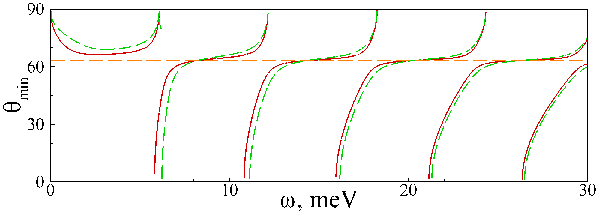
Perhaps the most interesting effects take place when [panels (b) and (e) in Figs. 8 and 9]. As expected, in the vicinity of the Brewster angle of the interface without graphene (), the polarization reflectance exceeds significantly that of polarized waves for all frequencies inside the band [compare dash-dotted lines in Figs. 8(e) and 9(e)], similar to the case of single graphene layer. However, it is not so for and inside the gaps. Here both polarizations exhibit an enhanced reflectance. Furthermore, we find some features specific for TM waves. As it has been shown in the previous section, the presence of graphene at the interface modifies the angle at which the reflectivity minimum in polarization occurs and this quasi-Brewster angle () is frequency-dependent [see Fig. 4(d)]. What happens to the minimum reflectivity angle, , when the wave is reflected from the graphene multilayer PC instead of the single interface? The answer follows from Fig. 10. When and belong to a band of allowed modes, oscillates around the conventional Brewster angle (, dashed horizontal line in the plot), except for the very low-frequency range ( meV), where the frequency dependence of the difference, , resembles that for the single graphene layer structure [compare to Fig. 4(d)]. The most striking feature in Fig. 10 is the divergence of for the frequencies corresponding to the stop–bands of the photonic crystal (compare to the middle column of Fig. 8).
The particularity of the situation [see panels (c) and (f) in Figs. 8 and 9] is the possibility to excite the polarized surface mode. If the angle of incidence is below the critical one (), the excitation of bulk PC modes takes place, while for , only the surface mode can be excited, as it can be seen by the low-frequency minima in the reflectivity spectra [see Figs. 8(c) and 8(f)]. A similar spectral shape has been observed experimentally in Ref. Sreekanth et al. (2012). One can say that the interface between the PC and the capping dielectric acts as an attenuated total internal reflection structure for single graphene layer, described in Ref. Bludov et al. (2010). It should be emphasized that the origin of the low-frequency minimum observed for polarized waves [Figs. 9(c) and 9(f)] is completely different. The former is a photonic crystal effect, while the latter exists also in the single-layer case [see Fig. 3(f)] and is unrelated to any PC surface mode.
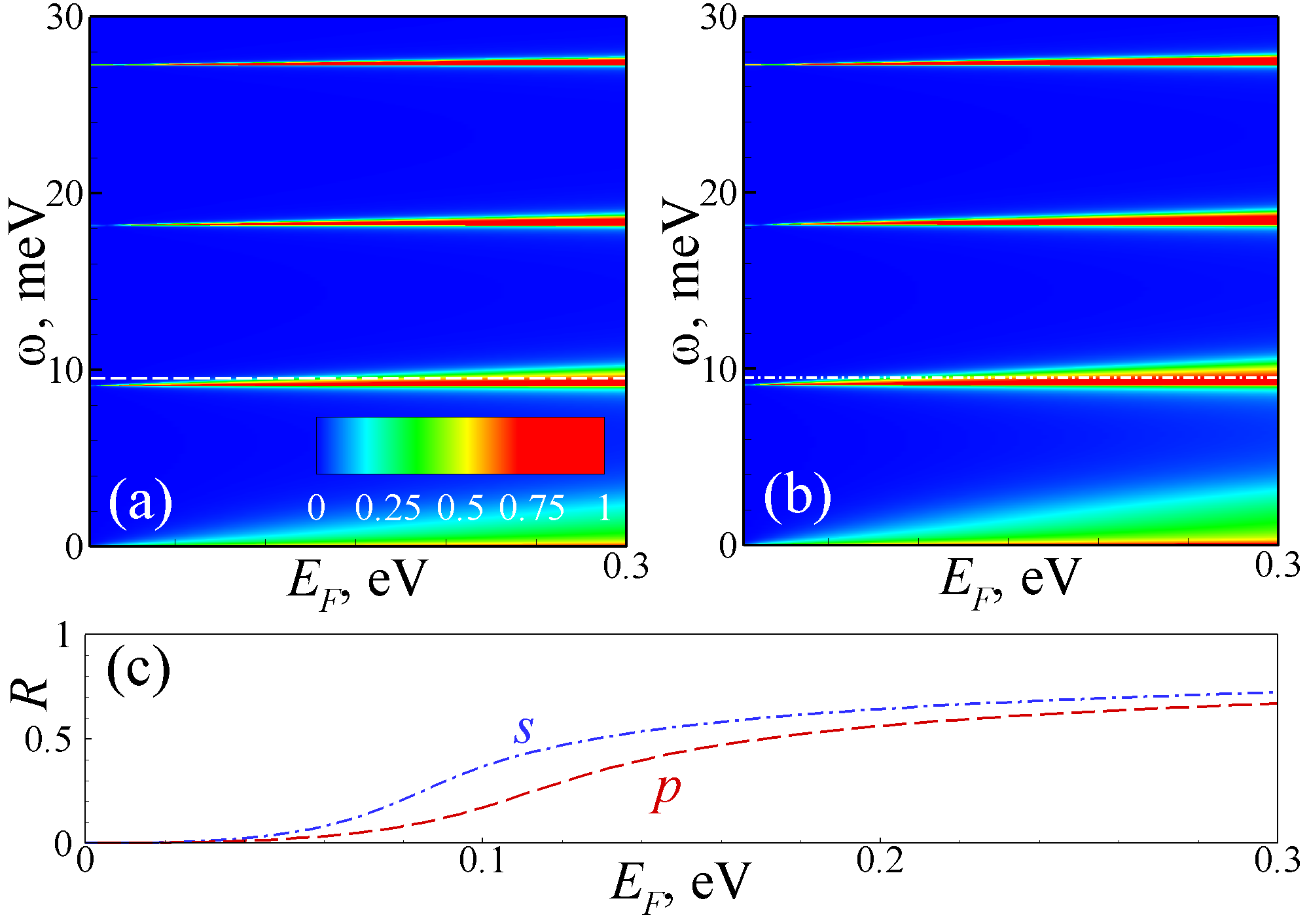
The possibility to change gap widths in the graphene multilayer PC spectrum by changing the Fermi level of graphene layers [see Fig.7] has an important consequence, the reflectance of the PC can be dynamically varied through the electrostatic gating, by changing the voltage applied to the graphene layers. This effect is depicted in Figs. 11(a) and 11(b) for and polarized waves, respectively. It can be used to design a tunable mirror. One has to choose the frequency of the incident wave inside one of the allowed bands, for a low Fermi energy, and inside the gap for a large . Then the reflectance of the structure can be varied in a broad range, as shown in Fig. 11(c). The dependence can be made even more abrupt using graphene layers with a smaller damping parameter .
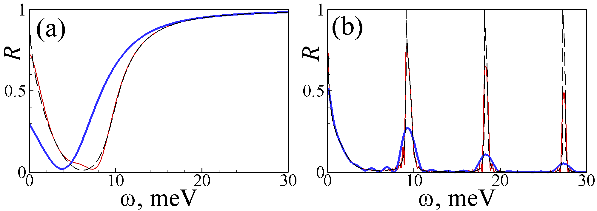
All the above results have been obtained for an infinite periodic stack of graphene layers. In reality, of course, PCs consist of a finite number () of layers. How does the value of affect the mode eigenfrequencies and the frequency dependence of the reflectance? As known from the band theory of crystalline solids, the eigenmode spectrum is quantized and corresponds to a discrete set of ”allowed” Bloch wavevectors, obtained from the usual Born–von Karman boundary conditions. For , the Bloch wavevector varies in a quasicontinuous way within the interval and Eqs. (46) and (47) hold with a very high precision. For relatively small values of , say, , the eigenmode band structure is washed away although the density of states retains a qualitative similarity with the case of . The ”stop-bands” are broadened and correspond to the maximum reflectivity well below the unity [see Fig. 12(b)], however, the latter increases rapidly with the number of layers, as known for periodically stratified media Born and Wolf (1980). Already for , the reflectance for polarized waves is very similar to that for infinite PC [compare dashed and thin solid lines in Fig. 12(b)].
Fig. 12(a) shows the finite size effect on the frequency dependence of reflectance related to the surface mode for polarization. No qualitative difference between the cases of and is seen [compare thick solid and dashed lines in Fig. 12(a)], which can be understood by the low dispersion of the surface-type PC mode with respect to the Bloch wavevector [see Fig. 5(b)]. This mode is, in fact, a Bloch-type surface plasmon-polariton (SPP) excitation induced by the incident wave when the attenuated total reflection conditions are met Bludov et al. (2013). The flatness of the dependence for this PC surface mode originates from the small overlap of the amplitudes of the SPP excitations in the different graphene layers.
IV Conclusions
In conclusion, there are several interesting effects related to the optical properties of graphene, which are revealed at oblique incidence. Some of them are expected already for a single graphene layer or just few of them. Under total internal reflection conditions at an interface between two dielectrics, the presence of graphene leads to EM energy absorption only for polarized waves. The absorbance attains its maximum exactly at the critical angle of incidence for polarization (and the maximum value is higher when the graphene conductivity is large), while it vanishes for polarization [Fig. 4(c)]. The minimum reflectance of polarized waves occurs at a (frequency dependent) quasi-Brewster angle that can differ by several degrees from the conventional Brewster angle for the same pair of dielectrics. Close to grazing incidence, graphene (when dielectric constants of substrate and capping layer are equal) is fully transparent to polarized waves and behaves like a mirror for polarization. This effect can be used for polarization-selective guidance of EM radiation. We have shown that a periodic stack of equally spaced parallel layers of graphene has the properties of a 1D photonic crystal, with narrow stop–bands that are nearly periodic in frequency. The PC properties are revealed also at oblique incidence. In particular, the stop–bands correspond to singularities of the minimum polarized reflection angle calculated as the function of frequency, which is an effect of potential interest for optical switching. We investigated the finite PC size effect and found that about 20 periods are sufficient to get the properties very close to those of the infinite PC. Finally, we should stress the possibility of tuning of the gaps’ (stop–bands’) width by changing the graphene conductivity via electrostatic gating, that would allow for dynamical variation of the reflectance at specific selected frequencies.
Acknowledgements
This work was partially supported by FEDER through the COMPTETE Program and by the Portuguese Foundation for Science and Technology (FCT) through Strategic Project PEst-C/FIS/UI0607/2011.
References
- Engheta and Ziolkowski (2006) N. Engheta and R. W. Ziolkowski, eds., Metamaterials - Physics and Engineering Explorations (IEEE Press, 2006).
- Han and Bozhevolnyi (2013) Z. Han and S. I. Bozhevolnyi, Rep. Prog. Phys. 76, 016402 (2013).
- Kravets et al. (2008) V. G. Kravets, F. Schedin, and A. N. Grigorenko, Phys. Rev. B 78, 205405 (2008).
- Joannopoulos et al. (2008) J. D. Joannopoulos, S. G. Johnson, J. N. Winn, and R. D. Meade, Photonic Crystals: Molding the Flow of Light (Second Edition) (Princeton University Press, 2008), 2nd ed.
- Garcia de Abajo (2007) F. J. Garcia de Abajo, Rev. Mod. Phys. 79, 1267 (2007).
- Xu et al. (2010) T. Xu, Y.-K. Wu, X. Luo, and L. J. Guo, Nature Communications 1, 59 (2010).
- Yablonovitch et al. (1991) E. Yablonovitch, T. J. Gmitter, and K. M. Leung, Phys. Rev. Lett. 67, 2295 (1991).
- Boardman et al. (2011) A. Boardman, V. Grimalsky, Y. Kivshar, S. Koshevaya, M. Lapine, N. Litchinitser, V. Malnev, M. Noginov, Y. Rapoport, and V. Shalaev, Laser & Photonics Reviews 5, 287 (2011).
- Vendik et al. (2012) I. Vendik, O. Vendik, M. Odit, D. Kholodnyak, S. Zubko, M. Sitnikova, P. Turalchuk, K. Zemlyakov, I. Munina, D. Kozlov, et al., Terahertz Science and Technology, IEEE Transactions on 2, 538 (2012).
- Liu et al. (2012a) A. Q. Liu, W. M. Zhu, D. P. Tsai, and N. I. Zheludev, Journal of Optics 14, 114009 (2012a).
- Chen et al. (2011) H. Chen, J. Su, J.Wang, and X. Zhao, Opt. Express 19, 3599 (2011).
- Figotin et al. (1998) A. Figotin, Y. A. Godin, and I. Vitebsky, Phys. Rev. B 57, 2841 (1998).
- Ozaki et al. (2002) M. Ozaki, Y. Shimoda, M. Kasano, and K. Yoshino, Adv. Mat. 14, 514 (2002).
- Li (2007) J. Li, Optics Communications 269, 98 (2007).
- Kee et al. (2000) C. Kee, J. Kim, H. Park, I. Park, and H. Lim, Phys. Rev. B 61, 15523 (2000).
- Park and Lee (2004) W. Park and J. B. Lee, Appl. Phys. Lett. 85, 4845 (2004).
- Han et al. (2012) M. G. Han, C. G. Shin, S.-J. Jeon, H. Shim, C.-J. Heo, H. Jin, J. W. Kim, and S. Lee, Adv. Mat. 24, 6438 (2012).
- Zu et al. (2012) P. Zu, C. C. Chan, T. Gong, Y. Jin, W. C. Wong, and X. Dong, Appl. Phys. Lett. 101, 241118 (2012).
- Savel’ev et al. (2005) S. Savel’ev, A. Rakhmanov, and F. Nori, Phys. Rev. Lett. 94 (2005).
- Savel’ev et al. (2006) S. Savel’ev, A. L. Rakhmanov, and F. Nori, Physica C 445, 180 (2006).
- Peres et al. (2006) N. M. R. Peres, F. Guinea, and A. H. Castro Neto, Phys. Rev. B 73, 125411 (2006).
- Falkovsky and Pershoguba (2007) L. A. Falkovsky and S. S. Pershoguba, Phys. Rev. B 76, 153410 (2007).
- Stauber et al. (2007) T. Stauber, N. M. R. Peres, and F. Guinea, Phys. Rev. B 76, 205423 (2007).
- Stauber et al. (2008a) T. Stauber, N. M. R. Peres, and A. H. Castro Neto, Phys. Rev. B 78, 085418 (2008a).
- Stauber et al. (2008b) T. Stauber, N. M. R. Peres, and A. K. Geim, Phys. Rev. B 78, 085432 (2008b).
- Gusynin et al. (2009) V. P. Gusynin, S. G. Sharapov1, and J. P. Carbotte, New J. Phys. 11, 095013 (2009).
- Grushin et al. (2009) A. G. Grushin, B. Valenzuela, and M. A. H. Vozmediano, Phys. Rev. B 80, 155417 (2009).
- Mishchenko (2009) E. G. Mishchenko, Phys. Rev. Lett. 103, 246802 (2009).
- Castro Neto et al. (2009) A. H. Castro Neto, F. Guinea, N. M. R. Peres, K. S. Novoselov, and A. K. Geim, Rev. Mod. Phys. 81, 109 (2009).
- Peres (2010) N. M. R. Peres, Rev. Mod. Phys. 82, 2673 (2010).
- Yang et al. (2009) L. Yang, J. Deslippe, C.-H. Park, M. L. Cohen, and S. G. Louie, Phys. Rev. Lett. 103, 186802 (2009).
- Peres et al. (2010) N. M. R. Peres, R. M. Ribeiro, and A. H. Castro Neto, Phys. Rev. Lett. 105, 055501 (2010).
- Ferreira et al. (2011) A. Ferreira, J. Viana-Gomes, Y. V. Bludov, V. M. Pereira, N. M. R. Peres, and A. H. Castro Neto, Phys. Rev. B 84, 235410 (2011).
- Liu et al. (2012b) J.-T. Liu, N.-H. Liu, J. Li, X. J. Li, and J.-H. Huang, Appl. Phys. Lett. 101, 052104 (2012b).
- Nair et al. (2008) R. R. Nair, P. Blake, A. N. Grigorenko, K. S. Novoselov, T. J. Booth, T. Stauber, N. M. R. Peres, and A. Geim, Science 320, 1308 (2008).
- Kuzmenko et al. (2008) A. B. Kuzmenko, E. van Heumen, F. Carbone, and D. van der Marel, Phys. Rev. Lett. 100, 117401 (2008).
- Mak et al. (2008) K. F. Mak, M. Y. Sfeir, Y. Wu, C. H. Lui, J. A. Misewich, and T. F. Heinz, Phys. Rev. Lett. 101, 196405 (2008).
- Wang et al. (2008) F. Wang, Y. Zhang, C. Tian, C. Girit, A. Zettl, M. Crommie, and Y. R. Shen, Science 320, 206 (2008).
- Kuzmenko et al. (2009) A. B. Kuzmenko, I. Crassee, D. van der Marel, P. Blake, and K. S. Novoselov, Phys. Rev. B 80, 165406 (2009).
- Crassee et al. (2011) I. Crassee, J. Levallois, A. L. Walter, M. Ostler, A. Bostwick, E. Rotenberg, T. Seyller, D. van der Marel, and A. B. Kuzmenko, Nat. Phys. 7, 48 (2011).
- Bao et al. (2011) Q. Bao, H. Zhang, B. Wang, Z. Ni, C. H. Y. X. Lim, Y. Wang, D. Y. Tang, and K. P. Loh, Nature Photonics 5, 411 (2011).
- Li et al. (2008) Z. Q. Li, E. A. Henriksen, Z. Jiang, Z. Hao, M. C. Martin, P. Kim, H. L. Stormer, and D. N. Basov, Nat. Phys. 4, 532 (2008).
- Bludov et al. (2010) Y. V. Bludov, M. I. Vasilevskiy, and N. M. R. Peres, Europhys. Lett. 92, 68001 (2010).
- Bludov et al. (2012a) Y. V. Bludov, M. I. Vasilevskiy, and N. M. R. Peres, Journal of Applied Physics 112, 084320 (pages 5) (2012a).
- Bludov et al. (2012b) Y. V. Bludov, N. M. R. Peres, and M. I. Vasilevskiy, Phys. Rev. B 85, 245409 (2012b).
- Hwang and Das Sarma (2009) E. H. Hwang and S. Das Sarma, Physical Review B 80, 205405 (2009).
- Svintsov et al. (2013) D. Svintsov, V. Vyurkov, V. Ryzhii, and T. Otsuji, Journal of Applied Physics 113, 053701 (2013).
- Stauber and Gómez-Santos (2012) T. Stauber and G. Gómez-Santos, Phys. Rev. B 85, 075410 (2012).
- Bludov et al. (2013) Y. V. Bludov, A. Ferreira, N. M. R. Peres, and M. I. Vasilevskiy, Int. J. Mod. Phys. B 27, 1341001 (2013).
- Eberlein et al. (2008) T. Eberlein, U. Bangert, R. R. Nair, R. Jones, M. Gass, A. L. Bleloch, K. S. Novoselov, A. K. Geim, and P. R. Briddon, Phys. Rev. B 77, 233406 (2008).
- Jovanović et al. (2011) V. B. Jovanović, I. Radović, D. Borka, and Z. L. Mišković, Physical Review B 84, 155416 (2011).
- Hajian et al. (2013) H. Hajian, A. Soltani-Vala, and M. Kalafi, Optics Communications 292, 149 (2013).
- Lee et al. (2011) J. Lee, K. S. Novoselov, and H. S. Shin, ACS NANO 5, 608 (2011).
- Sreekanth et al. (2012) K. V. Sreekanth, S. Zeng, J. Shang, K.-T. Yong, and T. Yu, Scientific reports 2, 737 (2012).
- Iorsh et al. (2013) I. V. Iorsh, I. S. Mukhin, I. V. Shadrivov, P. A. Belov, and Y. S. Kivshar, Phys. Rev. B 87, 075416 (2013).
- Ju et al. (2011) L. Ju, B. Geng, J. Horng, C. Girit, M. C. Martin, Z. Hao, H. a. Bechtel, X. Liang, A. Zettl, Y. R. Shen, et al., Nature Nanotechnology pp. 6–10 (2011).
- Nikitin et al. (2012a) A. Y. Nikitin, F. Guinea, F. J. Garcia-Vidal, and L. Martin-Moreno, Phys. Rev. B 85, 081405 (2012a).
- Hipolito et al. (2012) F. Hipolito, A. J. Chaves, R. M. Ribeiro, M. I. Vasilevskiy, V. Pereira, and N. M. R. Peres, Phys. Rev. B 86, 115430 (2012).
- Yan et al. (2012a) H. Yan, Z. Li, X. Li, W. Zhu, P. Avouris, and F. Xia, Nano letters 12, 3766 (2012a).
- Thongrattanasiri et al. (2012) S. Thongrattanasiri, F. H. L. Koppens, and F. J. García de Abajo, Phys. Rev. Lett. 108, 047401 (2012).
- Berman et al. (2010) O. L. Berman, V. S. Boyko, R. Y. Kezerashvili, A. A. Kolesnikov, and Y. E. Lozovik, Physics Letters A 374, 4784 (2010).
- Yan et al. (2012b) H. Yan, X. Li, B. Chandra, G. Tulevski, Y. Wu, M. Freitag, W. Zhu, P. Avouris, and F. Xia, Nature Nanotechnology 7, 330 (2012b).
- Nikitin et al. (2012b) A. Y. Nikitin, F. Guinea, and L. Martin-Moreno, Appl. Phys. Lett. 101, 151119 (2012b).
- Born and Wolf (1980) M. Born and E. Wolf, Principles of Optics (Pergamon Press, 1980).
- Goncalves et al. (2010) H. Goncalves, M. Belsley, C. Moura, T. Stauber, and P. Schellenberg, Appl. Phys. Lett. 97, 231905 (2010).
- Peres and Bludov (2013) N. M. R. Peres and Y. V. Bludov, Europhys. Lett. 101, 58002 (2013).