Stability and dopability of native defects and group-V and -VII impurities in single-layer MoS2
Abstract
We investigate the native defects, the Mo substitutional impurities of the group-VB and -VIIB elements, and the S substitutional impurities of the group-VA and -VIIA elements in single-layer MoS2, through density-functional theory calculations. It is found that the S-vacancy () and S-interstitial (Si) are low in formation energy, about 1 eV, in Mo- and S-rich conditions, respectively, but the carrier doping ability of the and Si is found to be poor, as they are deep level defects. The V, Nb, and Ta (group-VB) and Re (group-VIIB) impurities are found to be easily incorporated in single-layer MoS2, as Mo substitutional defects, where the V, Nb, and Ta are shallow acceptors and the Re is the only shallow donor among the considered. The unintentional -type doping in single-layer MoS2 exfoliated from the naturally grown MoS2 bulk materials is suggested to originate from the Re impurity.
A certain amount of defects and impurities are always present in natural single-crystalline materials. Even with the small imperfections, the electrical and optical properties of the materials can be largely deviated, and thus the understanding of the role of defects and impurities in the material properties is always important. The single-layer MoS2 has attracted a great deal of attention recently due to its unique electrical and optical properties STRANO12 . The single-layer MoS2 can be obtained from the mechanical exfoliation of the naturally grown MoS2 bulk materials KIS11 ; NOVOSEL04 ; NOVOSEL05 , and it shows a direct band gap semiconductor behavior HEINZ10 ; WANG10 ; KLEIN01 with typically unintensionally -type doped electrical conductivity KIS11 ; NOVOSEL05 .
The fundamental band gap of a single-layer MoS2 is 2.8 eV RAMASU12 ; LAMBRE12 . With the large exciton binding energy of about 0.9 eV, the optical band gap has been measured at 1.9 eV from the absorption and photo-luminescence spectroscopy HEINZ10 ; WANG10 . In -type single-layer MoS2 thin film transistors, the optically excited trions comprising two electrons and one hole have been also identified in presence of carrier electrons SHAN13 . Besides the large electronic correlation effects, the intrinsic broken inversion symmetry of the single-layer MoS2 induces the spin-orbit split bands at K and -K points in the hexagonal Brillouin zone SCHWINGEN11 and opens the new era of the spin- and valley-controlled electronics FENG12 ; CUI12 ; HEINZ12 ; LIU12 ; XIAO12 .
The practical application of the single-layer MoS2 is not trivial as well. The electron carrier mobility of the single-layer MoS2 has been measured to be as large as 200 cm2V-1s-1 in the HfO2/MoS2/SiO2 stacked thin film transistors KIS11 , while it is quite smaller, about 1 cm2V-1s-1, in the air/MoS2/SiO2 stacked structure NOVOSEL05 . Although the role of the encapsulating dielectric layers is not clear yet, the measured large electron mobility makes the single-layer MoS2 promising for the next generation high-speed electronics. For the electronics application of the single-layer MoS2, the efficient and controllable - and -type doping technology is an essential constituent.
In this study, we investigate the stabilities and the electrical dopabilities of the native defects of S-vacancy (), S-interstitial (Si), Mo-vacancy (), and Mo-interstitial (Moi); the Mo substitutional impurities of the group-VB (V, Nb, Ta) and the group-VIIB (Mn, Tc, Re) elements; and the S substitutional impurities of the group-VA (N, P, As, Sb) and the group-VIIA (F, Cl, Br, I) elements in single-layer MoS2, through density-functional theory (DFT) calculations. For the native defects, the and Si are found to be low in formation energy, about 1 eV, in Mo- and S-rich conditions, respectively, while the Mo-related defects of the and Moi have very high formation energies of above 2.5 eV. The carrier doping ability of the and Si is however found to be poor, as both the and Si are deep level defects. The group-VB impurities of V, Nb, and Ta, and the group-VIIB Re impurity as Mo substitutional defects are found to be negative in formation energy in S-rich conditions, by which their incorporation in single-layer MoS2 is facile. The V, Nb, and Ta are found to be shallow acceptors, and the Re is the only shallow donor impurity among the considered defects. Since Re is well known to exist in naturally grown MoS2 (molybdenite) via geochemical reactions since 2.91 gigayears ago (Ga) in the oxygenized earth subsurfaces HAZEN13 , the unintentional -type doping in single-layer MoS2 exfoliated from it is suggested to originate from the Re impurity.
Results
The calculated formation energies of the native defects and impurities are listed in Table 1. Among the native defects, the S-related defects of and Si are found to be low in formation energy. In Mo-rich limit condition, the most stable native defect is , of which formation energy is in the range of 0.70-1.48 eV depending on the Fermi level: 1.22 eV, when the Fermi level is at the VBM, and 0.70 eV, when the Fermi level is at the CBM. In S-rich limit condition, the Si is the most stable native defect, of which formation energy is in the range of 0.72-0.99 eV depending on the Fermi level. On the other hand, the Mo-related native defects are found to have very high formation energies above 2.5 eV, which indicates that the and Moi defects are rare in single-layer MoS2.
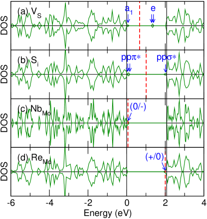
Thus, the abundant native defects in single-layer MoS2 are and Si in equilibrium, of which one is dominant is depending on the stoichiometry. The electronic density-of-states (DOS) of the and Si in the neutral charge state are shown in Fig. 1. For the , three defect states are induced inside the band gap. Since the has trigonal symmetry [Fig. 2(a)], the defect states are classified as a singlet state and doubly degenerate states. Due to the absence of an anion () in MoS2, two excess electrons occupy the state, and the two states are empty in the neutral charge state. The level is found to be located near the VBM, and thus it is not easy to generate carrier electrons from the . Instead, the empty levels are inside the band gap, as shown in Fig. 1(a), and thus the can be an electron trap center in single-layer MoS2. When the Fermi level is above the (0/-) transition level of +1.304 eV, the can trap an electron with ionized into , and when the Fermi level is above the (-/2-) transition level of +1.872 eV, the is ionizied into . When the Fermi level is near the VBM below the (+/0) transition level of +0.261 eV, the also can trap one hole with ionized into .
The Si is found to be also a deep level defect. When the Fermi level is near the VBM below the (+/0) transition level of +0.267 eV, the Si traps a hole (S), and when the Fermi level is near the CBM above the (0/-) transition level of +1.813 eV, the Si traps an electron (S). In a wide range of the Fermi level between the (+/0) and (0/-) transition levels, the Si exists in the neutral charge state (S). The atomic structure of the Si is shown in Fig. 2(b), in which the Si is located on top of a S atom on the single-layer MoS2. The S on-top configuration is found to be the lowest energy configuration for Si, where the configurations of the bridge between two S atoms and the hexagonal interstitial in the Mo layer are found to be much higher in energy than the S on-top configuration by 2.8 and 6.4 eV, respectively, in the neutral charge state. In the S on-top configuration, the Si forms a S-S bond with a host S atom [Fig. 2(b)]. As shown in Fig. 1(b), three defect states are generated by the Si; degenerated two are occupied and states near the VBM, and one is an empty state near the CBM [see Fig. 2(b)]. This electronic configuration of the S2--S is very similar to the peroxide (O) configuration NAHM12 . Since the level difference between the and is large, neither the excitation of the electrons nor the occupation of the level is unlikely in single-layer MoS2, unless the Fermi level is very close to the VBM or CBM. Thus, the Si is only a deep level defect without giving an efficient carrier doping in single-layer MoS2 even in high concentration of Si.

Where the carrier doping ability of the native defects in single-layer MoS2 is found to be poor, the impurities, which can be introduced in MoS2 either intentionally or naturally, are investigated. We consider the group-VA (N, P, As, Sb) and the group-VIIA (F, Cl, Br, I) elements as S substitutional impurities, and the group-VB (V, Nb, Ta) and the group-VIIB (Mn, Tc, Re) elements as Mo substitutional impurities. The formation energies and the electron transition levels are summarized in Table 1.
For acceptors, when the Fermi level is close to the VBM, the S substitutional NS, PS, AsS, and SbS impurities are unlikely to be incorporated in single-layer MoS2 in S-rich conditions by their high positive formation energies (see Table 1), which indicates that the N2 molecule, P triclinic metal, As2 molecule, and Sb trigonal metal forms are more stable than the doped configurations, respectively. In Mo-rich conditions, only when the Fermi level is near the CBM, the formation energies of the acceptor-like defects are found to be negative, and thus they can act as electron traps in the -type MoS2. When the Fermi level is close to the VBM, the formation energies of the NS, PS, AsS, and SbS are found to be positive even in the Mo-rich conditions, and thus their concentrations cannot be high in equilibrium. Thus, the -type doping ability of the group-VA impurities is low in single-layer MoS2. On the other hand, the group-VB impurities at the Mo substitutional sites have negative formation energies in S-rich conditions even when the Fermi level is close to the VBM, which indicates that the VMo, NbMo, and TaMo acceptors are easily incorporated in the -type single-layer MoS2. The (0/-) acceptor transition levels are found to be shallow for all the group-VB impurities, which are only 61, 29, 46 meV above the VBM for the VMo, NbMo, and TaMo, respectively. [For NbMo, the calculated DOS is shown in Fig. 1(c) and the charge density of the shallow acceptor level is shown in Fig. 2(c).] Therefore, we suggest that the V, Nb, and Ta impurities are efficient -type dopants in single-layer MoS2.
For donors, the S substitutional FS, ClS, BrS, and IS impurities can be incorporated in -type single-layer MoS2 in Mo-rich conditions, as hole compensating centers, with their negative formation energies (see Table 1). In -type single-layer MoS2, only the FS and ClS can be incorporated in Mo-rich conditions, as possible donors. In S-rich conditions, the formation energies are even higher. In any ways, all the S substitutional group-VIIA impurities are found to be deep donors with the (+/0) transition levels of 387, 160, 260, and 331 meV below the CBM for the FS, ClS, BrS, and IS, respectively. Based on their relatively high formation energies (except FS) and their deep donor characters, the FS, ClS, BrS, and IS are concluded to be not efficient for -type doping in single-layer MoS2. On the other hand, the donor-like Mo substitutional group-VIIB impurities of the MnMo, TcMo, and ReMo are found to be easily incorporated in -type single-layer MoS2, as they have negative formation energies in S-rich conditions (see Table 1). The (+/0) donor transition levels of the MnMo, TcMo, and ReMo are found to be 660, 208, and 61 meV below the CBM, respectively. The ReMo is found to be the only shallow donor impurity among them, and thus the Re impurity can be an efficient -type dopant in single-layer MoS2. [For ReMo, the calculated DOS is shown in Fig. 1(d) and the charge density of the shallow donor level is shown in Fig. 2(d).]
The presence of Re in naturally grown MoS2 bulk materials (molybdenite) has been well known in earth science. By the “Great Oxygenation Event” (GOE), the concentration of atmospheric oxygen had been increased during the Paleoproterozoic Era (2.5-1.6 Ga), and it had been furthermore increased following episodes of Neoproterozoic Era (1.0-0.541 Ga) glaciation KUMP08 . Both Mo and Re are insoluble in their more reduced tetravalent forms: Mo2+ and Re3+, whereas Mo6+ and Re7+ are more soluble in aqueous solutions and thus mobilized under more oxidizing conditions MILLER11 . The association of MoO, ReO, and SO in the dissolved phase and that of Mo, Re, and S as sulfides in the crust have been observed globally MILLER11 . The Re contents in molybdenite show overall increase from 832 ppm (1.631019 cm-3) to 10424 ppm (2.041020 cm-3) through time when the molybdenite was formed since 2.91 Ga HAZEN13 . Thus, the unintentional -type doping in single-layer MoS2 exfoliated from it is suggested to be due to the Re impurity.
In conclusion, the and Si native defects are suggested to be low in formation energy in Mo-rich and S-rich conditions, respectively, in single-layer MoS2, and their concentrations are expected to be high in thermal equilibrium. However, their carrier doping ability in single-layer MoS2 is not found to be strong, where the and Si act as deep trap centers for electrons and holes. The S substitutional group-VA and -VIIA impurities are neither found to be efficient - and -type dopants, because they have high formation energies to incorporate and/or deep level defect characters. It is suggested that the VMo, NbMo, and TaMo impurities can be efficient -type dopants, since they have low formation energies and are shallow acceptors. The ReMo is found to be the only shallow donor impurity among the considered and easily incorporated. For intentional -type doping in single-layer MoS2, the Re is suggested to be an efficient -type dopant. In naturally grown MoS2, a certain amount of Re impurities are known to exist, and then the single-layer MoS2 exfoliated from it can have the -type conductivity unintentionally by the naturally associated Re impurities.
Methods
We performed DFT calculations as implemented in the Vienna ab initio simulation package (VASP) code VASP1 ; VASP2 . The projector augmented wave (PAW) pseudopotentials PAW1 ; PAW2 and the local density approximation (LDA) LDA for the exchange-correlation energy of electrons were employed. The 88 supercell with 192 host atoms with the vacuum region of 18 Å was used for the single-layer MoS2, where the native defects and impurities were incorporated. A kinetic energy cutoff of 350 eV for the plane-wave expansion and a single -point at for the Brillouin zone integration were used. The atomic structures were relaxed until the Hellmann-Feynman forces were less than 0.02 eV/Å. The formation energies () of the native defects and impurities were calculated from
| (1) |
where is the defect with the charge state , is the total energy of the supercell containing the defect , is the number of element in the supercell (Mo, S, and impurity), is the chemical potential of the element , is the valence band maximum (VBM) level of the perfect single-layer MoS2, and is the Fermi level with reference to the VBM. The maximum we considered is the calculated LDA band gap of 2.06 eV, which corresponds to the conduction band minimum (CBM) level. For charged defects, the total energies were corrected to eliminate the spurious Madelung interactions between the supercells by -0.35 eV, obtained for our supercell structures. The and are correlated by , where is the total energy of the perfect single-layer MoS2 per a formula unit. For the Mo-rich limit condition, (Mo-metal), where (Mo-metal) is the DFT total energy of a Mo bcc metal per an atom. Then, . The heat of formation of a single-layer MoS2 calculated from is 1.44 eV. We set eV for convention, and then the range for stable single-layer MoS2 formation is -1.44 eV (Mo-rich limit) 0 eV (S-rich limit). The chemical potentials for the impurity atoms of V, Nb, Ta; Mn, Tc, Re; N, P, As, Sb; F, Cl, Br, I were obtained from the DFT total energies of a V bcc metal, a Nb bcc metal, a Ta bcc metal, an -Mn monoclinic metal, a Tc hcp metal, a Re hcp metal, a N2 molecule, a P triclinic metal, an As2 molecule, an Sb trigonal metal, a F2 molecule, a Cl2 molecule, a Br2 molecule, and an I2 molecule, respectively, per an atom.
References
- (1)
References
Acknowledgments
Acknowledgements.
This work was supported by Nano R&D Program through the National Research Foundation (NRF) of Korea (No. 2013-0042633).Author contribution
J.N. performed DFT calculations for native-defects, and M.P. performed DFT calculations for impurities. Y.K. conducted the research. J.N., M.P., and Y.K. wrote the manuscript. Y.K. is responsible for coordinating the project.
Additional information
Competing financial interests: The authors declare no competing financial interests.
| Groups | Defects | Formation energies (eV) | Transition levels (eV) | |||
|---|---|---|---|---|---|---|
| Mo-rich limit | S-rich limit | |||||
| VBM | CBM | VBM | CBM | |||
| Native defects | ||||||
| 1.48 (0) | 0.81 (-) | 2.92 (0) | 2.25 (-) | +0.261 (+/0) | ||
| 1.22 (+) | 0.70 (2-) | 2.66 (+) | 2.14 (2-) | +1.304 (0/-) | ||
| +1.872 (-/2-) | ||||||
| Si (on-top) | 2.43 (0) | 2.43 (0) | 0.99 (0) | 0.99 (0) | +0.267 (+/0) | |
| 2.16 (+) | 2.26 (-) | 0.72 (+) | 0.82 (-) | +1.813 (0/-) | ||
| 7.18 (+) | 6.50 (-) | 4.30 (+) | 3.62 (-) | +0.652 (+/-) | ||
| 5.70 (2-) | 2.82 (2-) | +1.178 (-/2-) | ||||
| 5.46 (3-) | 2.58 (3-) | +1.740 (2-/3-) | ||||
| Moi (split) | 3.36 (+) | 4.27 (0) | 6.24 (+) | 7.15 (0) | +0.370 (2+/+) | |
| 2.99 (2+) | 3.97 (-) | 5.87 (2+) | 6.85 (-) | +0.904 (+/0) | ||
| +1.686 (0/-) | ||||||
| Group-VA impurities | ||||||
| NS | 0.76 (-) | -1.40 (-) | 2.20 (-) | 0.03 (-) | +0.455 (0/-) | |
| 0.31 (0) | 1.74 (0) | |||||
| PS | 0.47 (-) | -1.70 (-) | 1.91 (-) | -0.26 (-) | +0.137 (0/-) | |
| 0.33 (0) | 1.77 (0) | |||||
| AsS | 0.80 (-) | -1.37 (-) | 2.24 (-) | 0.07 (-) | +0.087 (0/-) | |
| 0.71 (0) | 2.15 (0) | |||||
| SbS | 1.44 (-) | -0.72 (-) | 2.88 (-) | 0.72 (-) | +0.341 (0/-) | |
| 1.10 (0) | 2.54 (0) | |||||
| Group-VB impurities | ||||||
| VMo | 0.61 (-) | -1.56 (-) | -2.27 (-) | -4.44 (-) | +0.061 (0/-) | |
| 0.55 (0) | -2.33 (0) | |||||
| NbMo | 0.18 (-) | -1.98 (-) | -2.69 (-) | -4.86 (-) | +0.029 (0/-) | |
| 0.15 (0) | -2.72 (0) | |||||
| TaMo | 0.08 (-) | -2.08 (-) | -2.79 (-) | -4.96 (-) | +0.046 (0/-) | |
| 0.04 (0) | -2.84 (0) | |||||
| Group-VIIA impurities | ||||||
| FS | -3.62 (+) | -1.46 (+) | -2.18 (+) | -0.02 (+) | -0.387 (+/0) | |
| -1.85 (0) | -0.41 (0) | |||||
| ClS | -2.27 (+) | -0.10 (+) | -0.83 (+) | 1.34 (+) | -0.160 (+/0) | |
| -0.26 (0) | 1.18 (0) | |||||
| BrS | -1.86 (+) | 0.31 (+) | -0.42 (+) | 1.75 (+) | -0.260 (+/0) | |
| 0.05 (0) | 1.49 (0) | |||||
| IS | -1.42 (+) | 0.74 (+) | 0.02 (+) | 2.18 (+) | -0.331 (+/0) | |
| 0.41 (0) | 1.85 (0) | |||||
| Group-VIIB impurities | ||||||
| MnMo | 0.61 (+) | 2.77 (+) | -2.27 (+) | -0.11 (+) | -0.660 (+/0) | |
| 2.11 (0) | -0.76 (0) | |||||
| TcMo | -0.60 (+) | 1.57 (+) | -3.47 (+) | -1.31 (+) | -0.208 (+/0) | |
| 1.36 (0) | -1.52 (0) | |||||
| ReMo | -0.61 (+) | 1.56 (+) | -3.49 (+) | -1.32 (+) | -0.061 (+/0) | |
| 1.49 (0) | -1.38 (0) | |||||