3d transition metal impurities in diamond: electronic properties and chemical trends
Abstract
First principles calculations have been used to investigate the trends on the properties of isolated 3d transition metal impurities (from Sc to Cu) in diamond. Those impurities have small formation energies in the substitutional or double semi-vacancy sites, and large energies in the interstitial one. Going from Sc to Cu, the 3d-related energy levels in the bandgap move from the top of the bandgap toward the valence band in all three sites. Trends in electronic properties and transition energies of the impurities, in the substitutional or interstitial sites, are well described by a simple microscopic model considering the electronic occupation of the 3d-related levels. On the other hand, for the impurities in the double semi-vacancy site, there is a weak interaction between the divacancy- and the 3d-related orbitals, resulting in in vacancy- and 3d-related levels in the materials bandgap.
pacs:
61.72.Bb, 71.55.-i, 71.55.CnI Introduction
Silicon-based device technology has flourished over the last four decades. In such a time span, miniaturization was the keyword for improving device performance. When new challenges were foreseen in the horizon, designers used to find new solutions to overcome them end . In a near future, intrinsic physical limits of this technology may preclude further improvements keyes . A different route for electronic devices could be the use of wide bandgap semiconductors bun , since, when compared to silicon, they present superior materials properties for electronic devices, such as larger thermal conductivity, dielectric strength, and electron saturation velocity. There are still several technical limitations that prevent their competitiveness with the well established silicon technology. However, those materials have found their niche over the last decade, with applications in specific areas, such as high-power, high-temperature, high-frequency, opto-electronic gurbuz ; wide , and spintronic dutt ; kha devices.
There is currently a high demand for devices to operate under extreme conditions, and diamond is one of the leading candidates for such applications hud ; worth ; nich . This material has a wide bandgap (experimental value of 5.5 eV), high saturated carrier velocities, high electric field breakdown strength, low dielectric constant, and high thermal conductivity. Synthetic diamond has been grown out of graphite by high pressure-high temperature methods for about fifty years bundy being currently the most widely used growing process that allows to get macroscopic diamond samples. In those processes, 3d transition metal (TM) alloys, involving mainly nickel, cobalt, and iron, are used as solvent-catalysts to both overcome the sp2 to sp3 energy barrier and accelerate the growth process yelisseyev . Those TM end up being incorporated in the resulting diamond as residual impurities, either in isolated configurations or forming complexes with other defects, that can generate electrically and optically active centers yelisseyev ; larico12 . Several transition metal-related active centers have been experimentally identified in diamond, and have been associated to impurities in substitutional, interstitial, or double semi-vacancy configurations larico12 ; collins1 ; iakou ; nado . Understanding the nature and microscopic structure of those centers is crucial in developing diamond-related technologies.
Here, we used first principles total energy calculations to investigate the electronic properties and chemical trends of 3d TM-related centers (from Sc to Cu) in diamond. We focused on the trends of impurities in the substitutional, interstitial, or double semi-vacancy sites. The stability of those defects, in all three sites, were computed in terms of their formation energies. The electronic structure of this 3dn impurity family shows clear chemical trends in any site, with the 3d-related levels deepening from the top of the gap toward the valence band with increasing number (n) of 3d electrons. Additionally, we show that the respective electronic properties and transition energies could only be rationalized in terms of the number of electrons occupying the 3d-related energy levels within the materials bandgap.
II Methodology
The calculations were carried using the all-electron spin-polarized full-potential linearized augmented plane wave (FP-LAPW) method singh , implemented in the WIEN2k package blaha . The electron-electron interactions were described within the framework of the density functional theory and the generalized gradient approximation pbe . Calculations were performed considering a 54-atom reference FCC supercell and a Monkhorst-Pack () grid to sample the irreducible Brillouin zone mp . Convergence on the total energy was achieved using a plane wave basis set to describe the interstitial region, with the set limited by the wave number 7.0/R, where R = 1.2 a.u. (0.635 Å) is the radius of all atomic spheres. Self-consistent iterations were performed until convergence on the total energy of 10-4 Ry was achieved. In all systems with impurities, the internal degrees of freedom were optimized, without any symmetry constraints, until the force in each atom was smaller than 10-3 Ry/a.u. Such theoretical framework and convergence criteria have been shown to provide a reliable description of the electronic properties of defect centers in several semiconductors assali ; larico .
The formation energy of a TM impurity center in diamond () was computed by assali ; larico12 :
| (1) |
where is the total energy of a supercell with the defect in a charge state, with carbon atoms and TM impurity atoms. The and are the chemical potentials of respectively diamond and TM stable crystalline structures, computed within the same methodology described in the previous paragraph. Additionally, is the Fermi energy (, where is the bandgap energy ) and , where is a parameter that lines up the band structures of the bulk diamond material with and without the impurity in relation to the top of valence band of the pure crystal (). Within our theoretical approximations, we found eV for diamond.
For a certain impurity (in a substitutional, interstitial, or double semi-vacancy center), the transition energy between the and charge states, , is the value of the Fermi energy in the bandgap when the formation energies of the center in those respective charge states, as computed by equation 1, are equal.
| (2) |
We should stress that here we computed the transition energies, not the excitation ones, in which other methodologies could be more appropriate albu .
III Results and Discussion
We computed the properties of the 3d transition metal impurities in diamond, from Sc (atomic configuration ) to Cu (atomic configuration ), in three different sites: tetrahedral interstitial (TMi), substitutional (TMs), and double semi-vacancy (TM2V) ones.
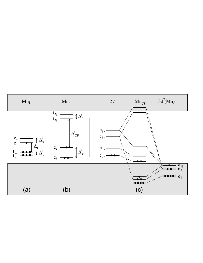
When a TM impurity, with a 3dn4s2 () atomic configuration, occupies a tetrahedral interstitial site in diamond (TMi), its 4s electrons are transferred to the 3d orbitals, resulting in a 3dn+2 configuration. In a tetrahedral crystal field, the 3d states are split into irreducible representations, with the threefold states lying lower in energy than the two-fold ones. This level ordering is the result of a strong octahedral crystal field created by the next nearest neighboring carbon atoms, that leads to a strong repulsion in the states, moving them up, in the upper half of the bandgap. Additionally, the crystal field energy splitting () is larger than the exchange splittings ( and ), such that the system always presents a low spin configuration. This results from the small lattice parameter of diamond, and is consistent with TM impurities in boron nitride bn . Figure 1(a) presents the specific case of Mni in the neutral charge state (3d7). For other TMi impurities in diamond (from Sc to Cu), their and levels have an equivalent behavior to those of Mni, but with a chemical trend such that those levels move all together from the midgap region, in Sci, toward the valence band, in Cui, consistent with results for TMi impurities in other semiconductors assali0 ; assali09 . The 3d-character localization in the TM atomic spheres increases with increasing the atomic number.
In the substitutional site (TMs), the impurity presents a 3dn-2 configuration, since four electrons are necessary for a covalent bonding with the four nearest neighboring carbon atoms. In contrast to the interstitial case, the tetrahedral crystal field drives the states to lie lower in energy than the ones. Here, the crystal field splitting also prevails over the exchange splittings (). Figure 1(b) presents the specific case of Mns in the neutral charge state (3d3). For other TMs impurities in diamond (from Sc to Cu), the and levels are equivalent to those of Mns, but with a chemical trend such that those levels move all together from the bandgap top, in Scs, toward the valence band, in Cus assali09 . The 3d-character localization in the TM atomic spheres also increases with increasing the atomic number.
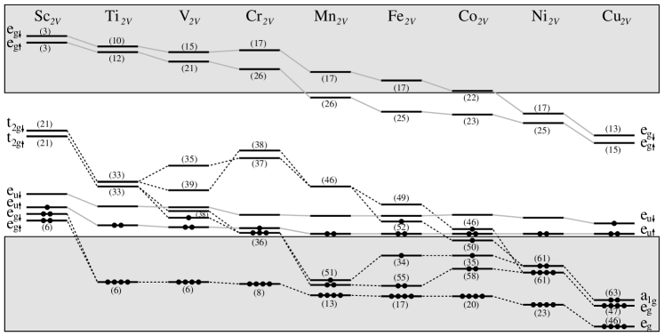
The electronic structure of the TM impurity in the double semi-vacancy site (TM2V) is considerably more complex than that in the other two sites. The electronic structure of TM2V centers are result of an interaction between the divacancy states with the ones coming from the atomic TM, as represented in figure 1(c) for the Mn2V center. The one-electron ground state structure of a diamond divacancy in D3d symmetry has the ee configuration in the bandgap region. In that symmetry, the TM 3d-related energy levels are split into 2eg+a1g. When a TM atom is placed in the middle position of a divacancy, one of its eg energy levels interacts slightly with the carbon dangling bonds, leaving a fully occupied non-bonding t2g-like (eg + a1g) orbital inside the valence band. However, the other TM-related eg orbital interacts with the divacancy-related eg gap state, resulting in an eg-bonding level in the valence band and an eg-anti-bonding one in the bandgap. The divacancy-related eu orbitals do not interact with any 3d-related TM ones, and consequently they remain near the top of the valence band.
For the TM2V center, depending on the impurity atomic number, the relative position of the 3d-related levels and the divacancy related ones may switch along the series, such that the electronic structure of each impurity depends strongly on such relative positions and the center charge state. Figure 2 presents the electronic structure of the TM2V, in the neutral charge state. The figure presents, in parenthesis, the 3d character inside the TM atomic sphere of each energy level. Going from Sc2V to Cu2V impurity centers, the 3d-t2g-related levels move from the middle of the bandgap toward the valence band, crossing with the divacancy-related eu ones, that lie near the valence band top. Additionally, the percentage of d-character increases along the series. These trends are consistent with those for substitutional and interstitial TM impurities. However, the electronic character of the highest occupied level of those centers depends on the relative position of the divacancy-related levels with respect to the 3d-related ones. According to figure 2 for the TM2V in the neutral charge state, it is associated to the TM for V, Fe, and Co, while it is associated to the divacancy for Sc, Ti, Cr, Mn, Ni, and Cu.
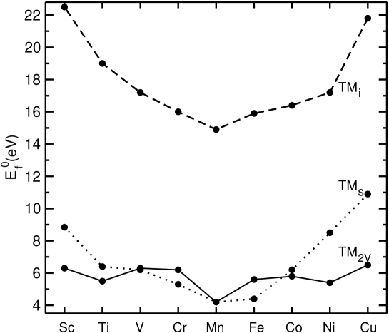
Figure 3 presents the trends on the formation energy for neutral impurities in all three sites, as computed by equation 1. The results show that the formation energies of a TM with 3dn or 3d10-n configurations are essentially equivalent in any site, with a clear energy favoring for the impurity in the middle of that family, which is manganese. Additionally, the interstitial site is the most unfavorable one for any TM, with formation energies of more than 10 eV higher than the respective ones in the other two sites larico . The small energy difference for the impurity in the substitutional or double semi-vacancy sites suggests that those two configurations may compete, co-existing in the diamond samples. We should also stress that trends in energy differences between TM defects in interstitial and substitutional configurations remain essentially the same for defects in charge states other than neutral. Those trends in energy are consistent, for example, with available experimental data for concentrations of cobalt yelisseyev and nickel nado ; larico12 impurities in as-grown and annealed synthetic diamond.
Table 1 presents the local symmetry and spin of the relaxed configuration for the TM impurities in the neutral charge state. As result of the electronic structures, the TM2V centers generally present spin values that are larger than the TMi and TMs centers. The manganese in the double semi-vacancy presents the largest spin of all centers (S=5/2). This large spin value suggests potential applications for spintronic devices jung ; lombardi .
Up to now, we have discussed the properties of the TM impurities in their neutral charge state. However, since those impurities introduce energy levels in the bandgap, both occupied and unoccupied ones, there is often a large number of possible stable charge states for each center. The transition energy between two different charge states is an important information for experimentalists to identify a certain center. Here, we carried out calculations for all stable charge states of each TM impurity in those three sites. Some centers presented up to seven different stable charge states, with transition energies lying in the diamond bandgap. The transition energy between two different charge states of a certain center was computed using the total energies of the centers in the initial and final charge states, as given by equations 1 and 2.
Our results indicated that the chemical trends on transition energies (computed by equation 2) along the 3d series, could only be rationalized if they were discussed in terms of the 3d-related level occupation and the respective crystal field and exchange splittings, as presented in figure 1. The comparison among different TM impurities should be conducted considering the same number of total electrons in each system, as discussed below. The transition energies within the diamond bandgap for TMs (from Sc to Cu) are shown in figure 4. The stable charge state of a certain center depends on the position of the Fermi level in the bandgap. For example, the Tis presents two transition states in the bandgap, the (0/-) and (-/2-), as shown in figure 4. This means that this center is stable in the neutral charge state for eV, in the negatively charge state for eV, and in the double negatively charge state for .
According to figure 1(b), the TMs impurity centers introduce energy levels with and irreducible representations, with and states below and ones. For an impurity with a 3dn4s2 atomic configuration, those levels are filled with d-electrons. For Sc center (), the and states are empty and the bandgap electronic configuration is , where the level ordering is consistent with the increasing values of the respective energy eigenvalues, as given in figure 1(b). The Sc center is related to adding one electron to an unoccupied level, leading to the bandgap electronic configuration. Therefore, the transition state is described by the connection between initial and final electronic configurations, as represented by . It could be represented in a compact form as , or just [] in figure 4. Accordingly, the transition state, or [], is related to the electronic configurations. For Scs, there is no additional transition state that lies in the bandgap.
For Tis, the () and () transition states are associated with and electronic configurations, respectively. Those two transition states should be compared respectively to the e transition ones of Scs center, that is why the transitions are connected by lines, as a guide to the eye, in figure 4.. Going to Vs, the same electronic configurations are observed, being now related to the () and () transition energies. However, the Vs center carried more two possible electronic configurations in the diamond bandgap, related to V and V centers, allowing to compute the transition energies between the electronic configurations (or in a compact form, ) and , associated with the () and () transition states, respectively. The Mns impurity has four stable charge states in the bandgap. For this impurity, after the and states are fully occupied, additional electrons could only occupy the states. For Mns, there is the transition, associated with the () one. From Cos to Cus, there are , , , and (or ) transitions. Therefore, one could associate, for example, the () transition of Scs with the () one of Tis and the () of Vs, i.e. transitions that involve the same number of electrons in the system. For all those centers, it is observed that any transition state has a chemical trend to move from the top of the bandgap in Sc toward the valence band maximum in Cu. Such trend is result of a Coulomb interaction, since the increasing atomic number, with a constant number of electrons, increases the nuclei-electron attractive interaction, reducing the total energy of the system.
Those results allow to establish a microscopic model for a transition energy, associated with the 3d level occupation in the bandgap. There is a small energy difference between the and transitions, which is associated with the occupation of the , being result of a Coulomb interaction. Now, there is a large energy difference between and transitions, which results from the exchange potential splitting (). This is because the transition differs from the one by the addition of an electron with a different spin. The large energy difference between the and transitions results from the presence of a strong crystal field splitting (), which is larger than the exchange potential splittings ( and ). For the transitions related to the occupation of the state (up to 3 electrons), the small energy difference is result of a Coulomb interaction. Finally, for the transition, the large energy difference is controlled by the exchange potential splitting of the state ().
The same model could be used to discuss the transition energies associated with TM impurities in the interstitial site, as presented in figure 5. According to figure 1(a), the TMi centers introduce energy levels with and irreducible representations in the bandgap, with and states below the and ones. For an impurity with a 3dn4s2 atomic configuration, those levels are filled with d-electrons. The first possible transition energy is associated to the electronic initial and final configurations . It could be represented in a compact form as , or just [] in figure 5. Those configurations are associated with the (3+/2+) and (4+/3+) transition states for the Sci and Tii impurities, respectively. After all the states are filled with increasing Fermi energy, the large energy difference for the electronic configurations (or in compact form ) is associated with the crystal field splitting (), consistent with the model of figure 1. For all those centers, it is observed that any transition state, along the 3d series, has a chemical trend to move from the upper half region of the bandgap, in Sc, toward the valence band maximum, in Cu. Additionally, the crystal field splitting for the TMi centers is considerably smaller than the respective splitting for the TMs ones ().
For the TM2V, this model could be applied only to a few transition states, since the almost non-interacting divacancy-related energy levels and the 3d-related ones lie in the same region of the bandgap, as shown in figure 2. As mentioned earlier, the divacancy-related states () remain in the bottom of the bandgap, the 3d-related states () move from the top of the gap in Sc toward the valence band in Cu. While some transition states are computed in association with electronic configurations filling the divacancy-related states, others are associated with filling the TM-related states. The transition energies associated with the TM2V centers are presented in figure 6. The trends can be here observed for some TM impurities. On the other hand, the V, Fe, and Co are exceptions, since the highest occupied level in their neutral charge state has a 3d-related character, as shown in figure 2. For those cases, the electronic configurations are considerably richer, which are presented in table 2 for several charge states. Therefore, table 2 helps to assign the electronic configurations associated with the respecive transitions. According to figure 6, in general, transition energies related to occupying the divacancy-related orbitals () are in the lower part of the bandgap while transition states associated to occupying the 3d-related states ( and ) are mostly in the upper part of the bandgap.
IV Summary
In summary, we have investigated the electronic properties and chemical trends of isolated 3d-transition metal impurities in diamond. We have shown that impurities in the substitutional or double semi-vacancy centers have smaller formation energies than the isolated centers in the interstitial site. We have also shown that trends on transition energies, for any of the three sites, could only be rationalized if they were discussed in terms of the increasing occupation of 3d-related states in the bandgap. Such trends are consistent with what would be expected for transition metal impurities in other semiconductors in either isolated configurations rae ; conti or forming complexes with other defects assali0 ; zhao .
Acknowledgments: The authors acknowledge support from Brazilian agencies CNPq and FAPESP. The calculations were performed in part using the computational facilities of the CENAPAD and the LCCA-CCE of the University of São Paulo.
References
- (1) M. Schulz, Nature (London) 399, 729 (1999).
- (2) R. W. Keyes, Rep. Prog. Phys. 68, 2701 (2005).
- (3) V. V. Buniatyan and V. M. Aroutiounian, J. Phys. D 40, 6355 (2007).
- (4) Y. Gurbuz, O. Esame, I. Tekin, W. P. Kang, and J. L. Davidson, Solid State Electr. 49, 1055 (2005).
- (5) Wide Bandgap Semiconductors: Fundamental Properties and Modern Photonic and Electronic Devices, eds. K. Takahashi, A. Yoshikawa, and A. Sandhu (Springer, Berlin, 2007).
- (6) M. V. G. Dutt, L. Childress, L. Jiang, E. Togan, J. Maze, F. Jelezko, A. S. Zibrov, P. R. Hemmer, and M. D. Lukin, Science 316, 1312 (2007).
- (7) A. A. Khajetoorians, B. Chilian, J. Wiebe, S. Schuwalow, F. Lechermann, and R. Wiesendanger, Nature (London) 467, 1084 (2010).
- (8) J. L. Hudgins, G. S. Simin, E. Santi, and M. A. Khan, IEEE Trans. Power Electr. 18, 907 (2003).
- (9) R. J. Nicholas, A. Mainwood, and L. Eaves, Philos. Trans. Royal Soc. A - Math. Phys. Eng. Sci. 366, 189 (2008).
- (10) C. J. H. Wort and R. S. Balmer, Mater. Today 11, 22 (2008).
- (11) F. P. Bundy, H. T. Hall, H. M. Strong and R. H. Wentorf, Nature (London) 176, 51 (1955).
- (12) A. Yelisseyev and H. Kanda, New Diam. Front. Carbon Tech. 17, 127 (2007).
- (13) R. Larico, J. F. Justo, W. V. M. Machado, and L. V. C. Assali, Phys. Rev. B 79, 115202 (2009).
- (14) A. T. Collins, Diamond Relat. Mater. 9, 417 (2000).
- (15) K. Iakoubovskii and A. T. Collins, J. Phys.: Condens. Matter 16, 6897 (2004).
- (16) V. A. Nadolinny, J. M. Baker, O. P. Yuryeva, M. E. Newton, D. J. Twitchen, and Y. N. Palyanov, Appl. Magn. Reson. 28, 365 (2005).
- (17) D. J. Singh, Planewaves, Pseudopotentials and the LAPW method (Kluver Academic, Norwell, 1994).
- (18) P. Blaha, K. Schwarz, G. Madsen, D. Kvaniscka, and J. Luitz, in WIEN2k, An Augmented Plane Wave Plus Local Orbitals Program for Calculating Crystal Properties, edited by K. Schwarz (Technical Universität Wien, Austria, 2001).
- (19) J. P. Perdew, K. Burke, and M. Ernzerhof, Phys. Rev. Lett. 77, 3865 (1996).
- (20) H. J. Monkhorst and J. D. Pack, Phys. Rev. B 13, 5188 (1976).
- (21) L. V. C. Assali, W. V. M. Machado, and J. F. Justo, Phys. Rev. B 69, 155212 (2004).
- (22) R. Larico, L. V. C. Assali, W. V. M. Machado, and J. F. Justo, Appl. Phys. Lett. 84, 720 (2004).
- (23) T. V. Albu, A. B. Anderson, and J. C. Angus, J. Electrochem. Soc. 149, E143 (2002).
- (24) L. V. C. Assali, W. V. M. Machado, and J. F. Justo, Appl. Phys. Lett. 89, 072102 (2006).
- (25) L. V. C. Assali and J. F. Justo, Phys. Rev. B 58, 3870 (1998).
- (26) L. V. C. Assali, W. V. M. Machado, and J. F. Justo, Physica B 404, 4515 (2009).
- (27) T. Jungwirth, J. Sinova, J. Masek, K. Kucera, and A. H. MacDonald, Rev. Mod. Phys. 78, 809 (2006).
- (28) E. B. Lombardi, Diam. Relat. Mater. 17, 1345 (2008).
- (29) H. Raebiger, S. Lany, and A. Zunger, Phys. Rev. B 79, 165202 (2009).
- (30) A. Continenza, G. Profeta, and S. Picozzi, Phys. Rev. B 73, 035212 (2006).
- (31) S. Zhao, L. V. C. Assali, J. F. Justo, G. H. Gilmer, and L. C. Kimerling, J. Appl. Phys. 90, 2744 (2001).
| Site | Sc | Ti | V | Cr | Mn | Fe | Co | Ni | Cu | |
|---|---|---|---|---|---|---|---|---|---|---|
| TMi | Sym. | Td | D2d | D2 | Td | D2d | Td | D2d | Td | D2d |
| S | 3/2 | 0 | 1/2 | 0 | 1/2 | 1 | 1/2 | 0 | 1/2 | |
| TMs | Sym. | D2d | Td | D2d | Td | D2d | Td | D2d | C1 | Td |
| S | 1/2 | 0 | 1/2 | 1 | 1/2 | 0 | 1/2 | 1 | 3/2 | |
| TM2V | Sym. | C2h | D3d | D3d | C2h | D3d | D3d | C2h | D3d | Ci |
| S | 3/2 | 1 | 3/2 | 2 | 5/2 | 2 | 3/2 | 1 | 1/2 |
| V2V | Fe2V | Co2V | ||||
| EC | S | EC | S | EC | S | |
| —— | — | —— | — | 3/2 | ||
| 1 | 5/2 | 2 | ||||
| 3/2 | 2 | 3/2 | ||||
| 1 | 3/2 | 1 | ||||
| 1/2 | 1 | 1/2 | ||||
| 1 | 1/2 | 0 | ||||
| 3/2 | 0 | —— | — | |||