Single Event Effect Characterization of the Mixed-Signal ASIC Developed for CCD Camera in Space Use
Abstract
We present the single event effect (SEE) tolerance of a mixed-signal application-specific integrated circuit (ASIC) developed for a charge-coupled device camera onboard a future X-ray astronomical mission. We adopted proton and heavy ion beams at HIMAC/NIRS in Japan. The particles with high linear energy transfer (LET) of 57.9 MeVcm2/mg is used to measure the single event latch-up (SEL) tolerance, which results in a sufficiently low cross-section of cm2/(IonASIC). The single event upset (SEU) tolerance is estimated with various kinds of species with wide range of energy. Taking into account that a part of the protons creates recoiled heavy ions that has higher LET than that of the incident protons, we derived the probability of SEU event as a function of LET. Then the SEE event rate in a low-earth orbit is estimated considering a simulation result of LET spectrum. SEL rate is below once per 49 years, which satisfies the required latch-up tolerance. The upper limit of the SEU rate is derived to be 1.3 events/sec. Although the SEU events cannot be distinguished from the signals of X-ray photons from astronomical objects, the derived SEU rate is below 1.3 % of expected non X-ray background rate of the detector and hence these events should not be a major component of the instrumental background.
keywords:
X-ray , ASIC , CCD camera , Single Event Effect1 Introduction
The X-ray charge-coupled device (CCD) cameras have been functioning as the primary focal plane detector of modern X-ray astronomy thanks to their well-balanced performances for imaging-spectroscopy [1, 2, 3]. Although we owe the imaging performance of a camera to the X-ray telescope, the energy and timing resolutions depend heavily both on the readout noise and on the processing speed of the front-end electronics, respectively. Since the forthcoming camera systems will require a larger number of pixels, a higher frame rate and a lower readout noise than those of the conventional systems, implementing the electronics with discrete integrated circuits (ICs) will dissipate too much power in orbit.
Recently, application-specific integrated circuits (ASICs) have been applied to the readout systems of the detectors including X-ray CCDs [4, 5, 6]. Drastically curtailed power consumption and compact size allow us to equip many chips next to the sensors. Hence we have developed the mixed-signal Complementary Metal Oxide Semiconductor (CMOS) ASIC as the signal processing electronics for CCD cameras in space use [7, 8]. It is characterized with not only a low-noise pre-amplifier but also a type analog-to-digital converter ( modulator), which has noise shaping capability [9]. The spectroscopic performance has been verified [10], which approved the ASIC as the front-end electronics of the X-ray CCD camera [11] onboard the ASTRO-H mission [12].
The radiation damages to space-use ICs are classified into two types: a total ionization dose (TID) effect and a single event effect (SEE). The former is the accumulating damage mainly due to the geomagnetically trapped protons and electrons. The latter is the stochastic damage that occurs when the energy deposited by a single heavy ion in the Galactic cosmic-rays exceed a threshold defined by the linear energy transfer (LET).
SEE can further be categorized into a single event latch-up (SEL) and a single event upset (SEU). SEL is a peculiar issue in CMOS Large Scale Integration (LSI). Since the NMOS and PMOS transistors are formed on a single silicon wafer, there are PNPN junctions forming parasitic thyristors [13]. If the input voltage exceeds that of the power supply momentarily due to the impingement of high energy particle, the thyristor is switched on and the excessive current continues to flow unless the power is shutdown. Finally, the LSI may be broken due to the overheat. On the other hand, SEU is generally represented by the bit inversion in the circuits such as memories and flip-flops. Despite the fact that SEU events are not critically harmful to the LSI, it can fudges up false signals.
Nakajima et al. [14] performed the TID test by irradiating our ASICs with a proton beam and verified that the gain and the input equivalent noise were not influenced up to 140 krad. The simulated dose rate in the low earth orbit (LEO) of ASTRO-H is 1 krad/yr, which promises no significant accumulating damage during the required mission lifetime of three years. This paper reports the SEE tolerance of the ASIC measured with protons and heavy ions.
2 Specification of the SEE Test
2.1 Specification of the ASIC
The detailed specification of our ASIC (hereafter we call it MND02) is described in Nakajima et al. [14] and references therein. Here we summarize its characteristics especially regarding the radiation hardness.
MND02 is equipped with four identical chains that process the signals from CCDs simultaneously. Each chain consists of a preamplifier, a 5-bit digital-to-analog converter (DAC), and two modulators (see Fig. 1 in [14]). Analog signals from CCD are fed into MND02 through AC coupling capacitor. Preamplifier differentially 10 times amplifies the signals and the 5-bit DAC gives offset to the signal level. Two modulators work by turns converting the amplified analog signals into two 155-bit serial streams [15]. Then the bit stream is decimation-filtered in subsequent circuits implemented in another ICs such as field-programmable gate arrays (FPGAs) and finally we obtain the 12-bit decimal value. The weighting coefficients for each bit in the decimation filter has been determined by simulations (Fi.g 6 in [7]) to enhance the frequency response as a low-pass filter and improve signal-to-noise ratio.
It was fabricated by Taiwan Semiconductor Manufacturing Company (TSMC) 0.35 m CMOS process through MOSIS service. The chip wafer is made from a p-type epitaxial wafer to improve the SEL tolerance. Although we do not employ the enclosed layout transistors, all the MOS toransistors are surrounded by guard rings to strengthen the chip against TID effect. 3 mm square bare chip is packed into 15 mm square ceramic quad flat package (CQFP). It functions with 3.3 V single power supply for analog and digital circuits. Fig. 1 shows the mask layout of MND02 with the labels of the circuit components. Most of the wafer area is devoted to capacitors.

|
2.2 Specification of the heavy ion beam
We employed the charged-particle beams at a physics-general experiment line 1 (PH1) and the medium energy beam (MEXP) course at Heavy Ion Medical Accelerator at Chiba (HIMAC) in National Institute for Radiological Sciences. Particles are extracted into the MEXP course immediately after the linear accelerator. The particle kinetic energy per atomic mass unit is 6 MeV/u. The beam duration is 350 sec and can be shortened by a chopper down to 5 sec. The pulse interval is 1.65 sec and hence the time profile of the beam is quite intermittent. The beam intensity is measured by the Faraday cup (FC) located at the upstream of our chamber. The device under test (DUT) is put in a vacuum state when we use MEXP course to avoid the energy loss and the scattering of the incident particles.
In the case we use PH1 course, the particles are accelerated in the synchrotron ring up to 400 MeV/u before they are extracted. Since the particles are fed to two rings by turns, the beam interval is 3.3 sec, while the duration of the beam on phase is 1 sec at the beam exit. DUTs are in an atmospheric pressure in PH1 course and are put 30 cm downstream from the beam exit that consists of Aluminum film with the thickness of 100 m. The energy loss in the flim and air is well below 0.1% of the incident energy. Beam fluxes were measured using a scintillation counter prior to each test.
Table 1 lists the specification of the beams adopted in the HIMAC. LET ranges from 5.8910-3 to 57.9 MeVcm2/mg. The beam size was measured by FC located near beam exit and the incident fluxes was derived by fitting the beam profile with a two-dimensional Gaussian model. There is no resin cover above the bare chip and the lid of the CQFP was removed throughout the test to ensure the incident energy. Since the size of the socket on which DUTs are mounted is 50 mm by 60 mm, the other ICs on the printed circuit board (PCB) were not exposed to the radiation.
We supply 3.3 V directly from transistor DC power supply unit (PSU) through no serial resistors. Hence the SEL causes immediate current increase up to the limit value. The current in the PCB during test and that of the limit are 0.13 and 0.2 A, respectively. The PSU was programed to shut down immediately when it noticed the current limit and supply voltage again after 5 seconds. We provided pseudo CCD signals into the DUT with a pixel rate of 78 kHz during the test.
| Species | Beam | Energy | Linear energy transfer | Beam Width | Maximum intensity | |
|---|---|---|---|---|---|---|
| course | (MeV/u) | (MeVcm2/mg) | (mm in FWHM) | (Ion/sec/cm2) | ||
| Proton | PH1 | 100 | 5. | 8910-3 | 3.8 1.1 | 1.7109 |
| Silicon | PH1 | 400 | 0. | 49 | 2.9 2.6 | 3.3104 |
| Krypton | PH1 | 200 | 4. | 72 | 4.4 3.8 | 3.3105 |
| Iron | PH1 | 400 | 1. | 68 | 7.1 5.7 | 3.3104 |
| Xenon | MEXP | 6 | 57. | 9 | 2.4 1.8 | 1.0108 |
| PH1 | 200 | 10. | 6 | diameter of 10 | 3.3106 | |
| PH1 | 400 | 7. | 2 | diameter of 10 | 3.3104 | |
3 Results of SEE Tests
3.1 Results of SEL Tests
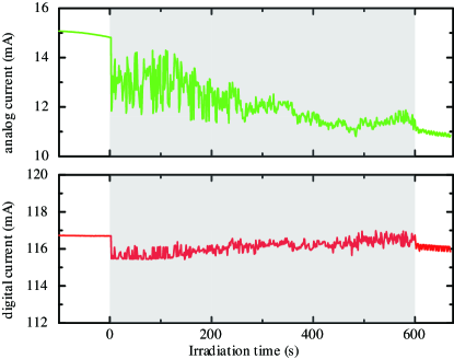
Fig. 2 shows the time profile of the current in the PCB for analog and digital circuit in the case of Xenon beam. The signal processing was performed throughout the duration shown in the figure. The current level during the beam on does not increase compared with that during beam off, which means there is no SEL during the irradiation. Total fluence of the Xenon ions was 7.21010 /cm2.
The cross-section of the SEL () is calculated dividing the number of the SEL events by the fluence of the particles. Since there was no SEL event in this experiment, we estimate the upper limit of using Poisson statistics. Assuming three SEL events for the above fluence, the derived is below cm2/(IonASIC) at 95 % confidence level. Nakajima et al. [14] also performed the SEL test for MND02 but only for Fe ions with the LET of 1.68 MeVcm2/mg. In this report we put the upper limit of at an LET by 34 times higher than that of the previous experiment. This LET is sufficiently high enough that SEL event should not be a cause of instrument downtime.
Although there is no significant increase of the current due to the beam, some features are seen in Fig. 2. The fluctuations of the current seen only when the beam was on can be understood that it is due to the ion-shunt [16, 17, 18]. It often follows from funneling [19, 20] in the drain depletion layer. When the carriers created by the charged particle concentrate throughout a volume linking two junctions, the coupling of the junctions occurs and then the carriers redistribute. This results in the temporal increase of the current in the chip. On the other hand, the current jump down when the beam sets in and the small fluctuations after the beam off cannot be explained by the ion shunt. Some charge up in the chip may explain the former phenomenon. Aside from the fluctuations, there is a slope in the current versus time. This comes from the other ICs than MND02 on the PCB since we see this slope not only in the radiation experiments but also in other experiments.
|
3.2 Results of SEU Tests
|
|
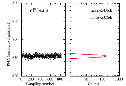
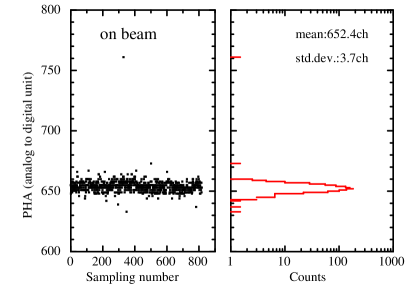
Fig. 3 shows the pulse height amplitude (PHA) distributions obtained when we process the pseudo CCD signals of 820 pixels with constant input voltage. While the distribution with beam off can be reproduced with Gaussian, there are some anomalous pixels whose PHA show significantly deviated values from the Gaussian when the Xenon 200 MeV/u beam is on. We regarded the pixels that deviates more than 4 from the distribution center as SEU events.
The influence of the SEU events on the PHA distribution varies considerably among the circuit components in MND02. If the bit inversion occurs at the resistor in the 5-bit DAC, all the pixels will be affected after the impingement until we set the DAC value again. Assuming that the digital circuit in the final stage of modulator is hit, one of the 155 output bit stream is inverted. Then the expected deviation from the normal PHA depends on the weighting coefficient of the inverted bit and it is no more than 8 % of the normal value [7], which corresponds to 50 units in the case of Fig. 3. In cases where big amounts of electron-hole pairs are created in the capacitors of the preamplifier or the integrator in the modulators, the amount of the PHA deviation from the normal value depends on the energy deposited in the chip. Then only the single pixel is affected since we assert a reset signal to both of the preamplifier and the modulator. Considering the fact that the amount of the PHA deviation from the distribution ranges from 20 to 120 units and the fact that the anomalies do not last over pixels, we guess that the probable components affected are the capacitors lying scattered over the chip.
4 Estimation of the SEE Tolerance
4.1 LET spectrum in the LEO
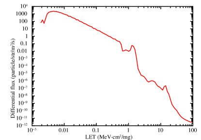
The SEE event rate of an electronic devices in the specific orbit and duration is estimated by integrating the product of the LET flux and SEE cross-section. The energies, densities and types of particles in the space environment depend significantly on the orbital parameters such as the altitude, the inclination angle, the recent solar activity, and the amount of spacecraft shielding. Then we simulated the LET flux distribution due to the galactic cosmic-rays in the LEO of our primary target mission ASTRO-H using the tools provided by JAXA Space Environment & Effects System (SEES) group 111http://seesproxy.tksc.jaxa.jp, which is shown in Fig. 4. In this simulation Cosmic Ray on Micro-Electronics (CREME) code [21] is used. In this mission MND02 chips are mounted on a PCB in the camera body that is made of Aluminum with the thickness of about 20 mm.
|
4.2 Estimation of SEE rate
The probability of SEE when a charged particle impact the LSI is expressed as a function of LET () as following equation called Weibull curve.
| (1) |
where is the saturated probability, is the threshold LET, and is a curve width. Then we calculate the SEE rate integrating the product of and particle flux throughout the available LET range in Fig. 4 of 2.0 100 MeVcm2/mg.
Although series resistors are implemented in power lines for the flight model electronics to avoid the thermal destruction in the case of the SEL, we require the probability for the latch-up to be below once per 30 yrs, which is 10 times the required mission lifetime of ASTRO-H. Since we put the upper limit of the SEL probability using Xenon beam of 6 MeV/u, the most pessimistic estimation of SEL rate is cm2/(IonASIC) for 2.0 57.9 MeVcm2/mg and for 57.9 100 MeVcm2/mg. Then the SEL rate is calculated to be once per 1.5 sec or 49 yrs, which satisfies the requirement.
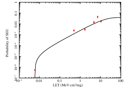
The SEU rate can be estimated in the same manner as that for SEL. However, we need an additional care about the proton data because of the nuclear reactions between high-energy protons and silicon nuclei in the device. Protons indirectly induce SEUs since their elastic and inelastic interactions create secondary projectiles. They consist of neutrons, alpha particles and heavy recoiling ions [22]. The resultant LET distribution in the silicon wafer is not a -function but wide-spread function.
Hence we desire to calculate the number of SEU events due to the secondary heavy ions and subtract it from the total number of SEUs in the proton test. Since we measured the SEU probability at the LET of Si 400 MeV/u (), it is assumed that the secondary particles with the LET larger than induce SEUs with the same probability as . On the other hand, when the LET of the secondary particle is smaller than , we regard the SEU as that due to the proton. We adopted the LET distribution calculated by Barak [23] in which 410-5 of the total number of protons create the secondary heavy ions whose LETs are larger than .
|
Taking into account the above consideration, we fitted the SEU probability plot with the Weibull function (Fig. 5). The best fit values are 5.6810-3 MeVcm2/mg for , 3.88610-2 for , and 15.3 MeVcm2/mg for . We then estimated the SEU event rate using fitted parameter to be 8.010-6 SEU/sec.
Nevertheless the sharpness of the rising edge in Weibull function strongly depends on this estimation, the number of the data below 1 MeVcm2/mg is limited in our experiment. Therefore we estimate the systematic error as follows considering that the Weibull function is monotonically increasing. In the worst case estimation, the probability of SEU in an LET range higher than a data point and lower than the next one is assumed to be that of the latter data point. In this way we estimated most pessimistic rate to be 1.3 SEU/sec.
Most of the SEU events such as that in Fig. 3 cannot be distinguished from the signals due to X-ray photons from astronomical objects. This means we need to consider the SEU event as a part of the non X-ray background (NXB). The NXB intensity of the X-ray CCD Camera onboard ASTRO-H is expected to be similar to that of the X-ray Imaging Spectrometer onboard Suzaku satellite, which is 0.1 counts/sec [24]. Since the upper limit of the SEU rate is below 1.3 % of known NXB rate, it should not be a major component of the instrumental background.
5 Conclusion
We have developed an mixed-signal ASIC for the readout circuit of the onboard CCD camera. The results of the radiation tolerance test for SEE using protons and heavy ion beams can be summarized as follows
-
1.
We detected no SEL events even with a high LET beam of Xenon 6 MeV/u. The upper limit of the cross-section is cm2/(IonASIC). The flapping of the current seen only when the beam was on can be understood such that it is due to the ion-shunt.
-
2.
Some anomalous pixels that have peculiar PHA are seen only when the beam is on, which we regard as SEU events. The most probable location of the impingement is capacitors in the preamplifier and the integrator of the modulators.
-
3.
The SEE event rate in an LEO is estimated by integrating the product of the simulated LET flux spectrum and SEE probability. The upper limit of the SEL rate is once per 49 years, which satisfies our requirement. The upper limit of the SEU rate is derived to be 1.3 events/sec, which is 1.3 % of known NXB rate.
Acknowledgment
We acknowledge people of Accelerator Engineering Corporation, especially Satoshi Kai who offered us much supports in the radiation damage experiment. We used the simulation tools provided by SEES group in JAXA. This work is supported by the Nano-Satellite Research and Development Project in Japan , the Research Project with Heavy Ions at NIRS-HIMAC, and the JSPS KAKENHI Grant Number 22740122, 23000004, and 24684010.
References
- [1] M. C. Weisskopf, B. Brinkman, C. Canizares, G. Garmire, S. Murray, L. P. Van Speybroeck, Publ. Astron. Soc. Pacific, 114 (2002) 1
- [2] F. A. Jansen and XMM Science Operations Team, American Astronomical Society 32 (2000) 724
- [3] K. Mitsuda, et al., Publ. Astron. Soc. Japan 59 (2007) 1
- [4] R. Rando, A. Bangert, D. Bisello, A. Candelori, P. Giubilato, M. Hirayama, R. Johnson, H. F. -W. Sadrozinski, M. Sugizaki, J. Wyss, M. Ziegler, IEEE Trans. Nucl. Sci., 51 (2004) 1067
- [5] H. Tajima, T. Nakamoto, T. Tanaka, S. Uno, T. Mitani, Ed. Ce. Silva, Y. Fukazawa, T. Kamae, G. Madejski, D. Marlow, K. Nakazawa, M. Nomachi, Y. Okada, T. Takahashi, IEEE Trans. Nucl. Sci., 51 (2004) 842
- [6] S. Herrmann, W. Buttler, R. Hartmann, P. Holl, N. Meidinger, L. Strueder, Nucl. Sci. Symposium Conference Record IEEE vol.3 (2007) 2398
- [7] D. Matsuura, H. Nakajima, E. Miyata, H. Tsunemi, J. P. Doty, H. Ikeda, Proc. SPIE 6686 (2007) 66860L
- [8] H. Nakajima, D. Matsuura, N. Anabuki, E. Miyata, H. Tsunemi, J. P. Doty, H. Ikeda, T. Takashima, H. Katayama, IEEE Trans. Nucl. Sci. 56 (2009) 747
- [9] H. Inose, Y. Yasuda, J. Murakami, IRE Transactions on Space Electronics Telemetry SET-8 (1962) 204
- [10] H. Nakajima, D. Matsuura, N. Anabuki, E. Miyata, H. Tsunemi, J. P. Doty, H. keda, H. Katayama, Nucl. Instr. and Meth. A 610 (2009) 78
- [11] K. Hayashida et al., Proc. SPIE 8145 (2011) 814505
- [12] T. Takahashi et al., Proc. SPIE 7732 (2010) 77320Z
- [13] B. L. Gregory, B. D. Shafer, IEEE Trans. Nucl. Sci. 20 (1973) 293
- Nakajima et al. [2011] H. Nakajima, D. Matsuura, T. Idehara, N. Anabuki, H. Tsunemi, J. P. Doty, H. Ikeda, H. Katayama, H. Kitamura, Y. Uchihori, Nucl. Instr. and Meth. A 632 (2011) 128
- [15] J. P. Doty, D. Matsuura, H. Ozawa, E. Miyata, H. Tsunemi, H. Ikeda, Proc. SPIE 6276 (2007) 62761P
- [16] J. R. Hauser, S. E. Diegl-Nagle, A. R. Knudson, A. B. Campbell, W. J. Stapor, P. Shapiro, IEEE Trans. Nucl. Sci. 32 (1985) 4114
- [17] A. R. Knudson, A. B. Campbell, J. R. Hauser, M. Jessee, W. J. Stapor, P. Shapiro, IEEE Trans. Nucl. Sci. 33 (1986) 1560
- [18] A. O. Brown, B. Bhuva, S. E. Kerns, W. J. Stapor, IEEE Trans. Nucl. Sci. 40 (1993) 1918
- [19] C. M. Hsieh, P. C. Murley, R. R. O’Brien, IEEE Electron Device Lett. 2 (1981) 103
- [20] A. B. Campbell, A. R. Knudson, W. J. Stapor, P. Shapiro, S. E. Diehl, J. Hauser, IEEE Trans. Nucl. Sci. 32 (1985) 4128
- [21] J. H. Adams, Jr., R. Silberberg, C. H. Tsao, Navy Research Laboratory Memorandum Report 4506 (1981)
- [22] A. Akkerman, J. Barak, J. Levison, Y. Lifshitz, Radiation Physics and Chemistry 48 (1996) 11
- Barak [2001] J. Barak., IEEE Trans. Nucl. Sci. 48 (2001) 1937
- [24] K. Koyama et al., Publ. Astron. Soc. Japan 59 (2007) 23