Electronic transport of folded graphene nanoribbons
Abstract
We investigate the electronic transport properties of a folded graphene nanoribbon with monolayer nanoribbon contacts. We consider two possible foldings: either the nanoribbon can be folded onto itself in the shape of a hairpin with the nanoribbon leads at a angle, or the monolayer contacts have different directions, forming a angle. The system is described by a single -band nearest-neighbor tight-binding Hamiltonian taking into account curvature effects. We have found that for the case of a nanoribbon folded over itself the conductance oscillates from almost zero and a finite value depending on the coupling between contacts, whereas in the angle folding the conductance is only slightly perturbed, allowing for the connection of graphene nanoelectronic components in a variety of geometries.
I Introduction
Graphene is an one-atom-thick covalently-bonded carbon layer ordered in a honeycomb lattice. It has been recently isolated and shown to be stable under room conditions Novoselov et al. (2004), giving rise to the exploration of its fascinating properties. As it is an ambipolar material, the charge carrier type can be changed by applying a gate voltage; furthermore, the high mobility of charge carriers Castro-Neto et al. (2009) due to the absence of backscattering. These characteristics point at graphene as an interesting alternative for novel nanoelectronic devices. However, as graphene is a zero-gap material, it cannot be employed for the fabrication of diodes and most electronic components, for which an electronic gap is essential. Thus, there has been substantial interest in controlling the electronic properties of graphene by quantum size effects. For example, cutting graphene into quasi-one-dimensional nanoribbons Han et al. (2007) produces electronic gaps. Another route to produce a gap is to stack two graphene layers. Bilayer graphene Castro et al. (2007); Nilsson et al. (2007); Min et al. (2007); González et al. (2010a) holds huge potential because it is a gate-tuneable semiconductor, Guinea et al. (2006); McCann and Fal’ko (2006) as observed in electronic transport Castro et al. (2007); Gava et al. (2009) and in photoemission experiments Ohta et al. (2006).
Due to the planar geometry of graphene, large-scale integrated circuits made by nanolitographic techniques can be envisioned. Indeed, there are numerous studies on the transport properties of graphene nanoribbon bends and junctions such as those that may occur in graphene-based nanoelectronics. For certain angles and ribbon geometries, the conductance can be completely suppressed, and in certain cases, conductance oscillations due to multiple resonances may appear Iyengar et al. (2008).
In order to avoid undesirable conductance gaps, we propose to use folded ribbons as contacts. On the one hand, it allows integration in the vertical direction, since the ribbon can connect stacked graphene components. On the other hand, using a sufficiently long ribbon, it can serve as a connector at different angles without a conductance gap.
In this work we present a theoretical study of the conductance through folded metallic armchair graphene nanoribbons (aGNR). Such fold terminations for bilayer graphene have been experimentally observed: studies of heat treated graphite using high resolution TEM images show a predominance of closed edges between layers of graphene and a large proportion of AA stacking Liu et al. (2009). Furthermore, folds and bends on narrow carbon nanoribbons have also been reported Li et al. (2008). From the theoretical viewpoint, the electronic structure of folded graphene has been studied Takagi and Okada (2010). The transport properties of folded graphene ribbons along the fold direction have also been reported without considering curvature effects Xie et al. (2009); besides, the transport in a uniform magnetic field has also been explored Prada et al. (2010), but the emphasis was in the effective change of direction the magnetic flux when moving across the fold, and no curvature effects nor interlayer coupling were considered.
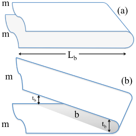
We consider the folded ribbon to be composed of a curved portion, also called fractional nanotube, Huang et al. (2009); Feng et al. (2009a) and two armchair graphene ribbons with a finite overlap region, as depicted schematically in Fig. 1. We explore the role of curvature and interlayer coupling on the conductance, showing that folded ribbons can be employed as metallic contacts provided that the effective bilayer region is minimized. The geometries studied are the following: (i) a nanoribbon folded onto itself, in the shape of a hairpin, so that the electrode ribbons are on top of each other, oriented at a angle, shown in Fig. 1(a); (ii) the ribbon is folded in such a way that the electrode ribbons are at a angle, depicted in Fig. 1(b). We choose this angle in order to achieve an AA stacking in the bilayer region formed by the overlapping electrodes. Other angles can be considered with a different bilayer stacking, but for the sake of simplicity we restrict ourselves to the most symmetric case which has been recently observed to experimentally appear in bilayer graphene Liu et al. (2009).
II Theoretical description of the system
II.1 Tight-binding Hamiltonian
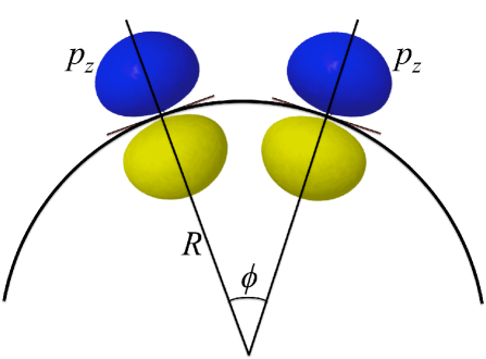
The low-energy transport properties of planar graphene are well described within a single -band tight-binding approximation with nearest-neighbor in-plane hopping given by the parameter 3 eV. This model only considers the and bands due to the hopping between orbitals perpendicular to the graphene plane. In the fractional nanotube region, we must consider the effect of curvature. As its main consequence is the misalignment of the orbitals, we model it by assuming that the hopping integral between neighbor atoms is changed with respect to that of planar graphene, The curvature-modified hopping is proportional to the cosine of the misalignment angle between orbitals, , with defined in Fig. 2 Kleiner and Eggert (2001).
The region where the two ribbons overlap is just a finite-size fragment of bilayer graphene with AA stacking. In the case of folding at , the bilayer region is a rectangular flake of length . For nanoribbons folded at , the bilayer flake has a triangular shape, as depicted in Fig. 1 (a), with size depending on the ribbon width. The interlayer coupling is modeled with a single hopping connecting atoms directly on top of each other, which we take as , in agreement with experimental results Ohta et al. (2006); Malard et al. (2007).
In the bilayer with AA stacking all the atoms of layer are on top of the equivalent atoms of layer . We assume that all atoms bottom layer are connected to those on the the upper layer located exactly on top of them; thus, the Hamiltonian takes the form
| (1) | |||||
where annihilates an electron on sublattice , in plane , at lattice site . The subscript represents a pair of in-plane nearest neighbors. The second term in Eq. (1) represents the interlayer hopping.
II.2 Landauer-Büttiker formalism
We calculate the electronic and transport properties using the surface Green function matching method Chico et al. (1996); Nardelli (1999). Thus, the system is partitioned in three blocks: two semi-infinite leads, which we assume to be semi-infinite aGNRs, and the conductor, consisting of the bilayer and the folded region. The Hamiltonian of the system can be partitioned as
| (2) |
where , , and are the Hamiltonians of the central portion, left and right leads respectively, and , are the coupling matrix elements from the left and right lead to the central region . The Green function of the conductor is
| (3) |
where is the selfenergy due to lead , and is the Green function of the semi-infinite lead González et al. (2009).
III Results
III.1 Nanoribbons folded at
We first focus on an armchair graphene nanoribbon folded onto itself in the shape of a hairpin, i.e., in a configuration where the relative angle between the bottom and top leads is (Fig.1(a)). Here we need to consider two effects: the layer-layer coupling which depends on the length of the overlapping region, and the effects of the curved portion, modeled as a fractional nanotube. We assume our leads are noninteracting monolayer graphene nanoribbons, so that the bilayer region with interlayer coupling has a finite size , given in terms of the armchair unit cell size length. The width of the nanoribbon is given by the number of dimers across its width, N.
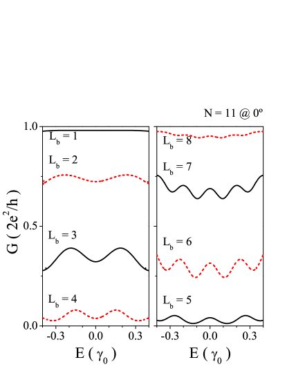
For an armchair nanoribbon folded at , the curved edge has to be a fractional armchair nanotube (faCNT). In this work we model the curved edge as a section of a (4,4) armchair carbon nanotube. In Figure 3 we show the conductance of the aGNR of width N = 11 folded at as a function of Fermi energy for several bilayer lengths . Notice the periodic behavior in the conductance as a function of the energy, due to the multiple interferences produced in the bilayer region. These periods change with the system size. Besides, there is another periodicity related to the bilayer portion , roughly equal to 8 unit cells. These periodicities in the electronic conductance are also observed with equal frequencies in wider aGNR ribbons folded at , such as the N=17 case (not shown here because in the depicted energy range their conductances are equal, given that they only have one conductance channel at that energy interval). The oscillations are reminiscent of those found in the transmission through bilayer flakes González et al. (2010a), where the conductance was demonstrated to depend on both the energy and the size of the scattering region.
III.2 Nanoribbons folded at
For the configuration, the folded edge for an armchair nanoribbon has to be a fractional zigzag nanotube (fzCNT) in order to maintain the AA stacking in the bilayer region. The radius of the fzCNT depends on nanoribbon width, and close to nm, to be consistent with previous ab-initio calculations Feng et al. (2009a).
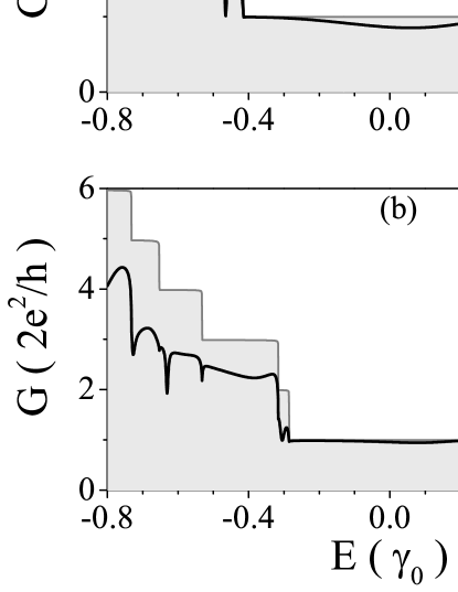
In figure 4 (a), we show the conductance as a function of Fermi energy for aGNR N = 11 at with a fzCNT (8,0). The bilayer region for this case consists of a triangle, as shown in Fig.1(b). The most relevant change with respect to to hairpin geometry is that the electron-hole symmetry is broken. This is due to the mixing of the two sublattices produced by the interlayer hopping: when the two nanoribbon electrodes are at , the hopping in the bilayer region produces odd-numbered carbon rings comprising atoms of the bilayer and the fractional nanotube region. This did not happen when the contacts were at , thus yielding e-h symmetric conductances, like those previously shown in Fig. 3.
In figure 4 (b) we show the conductance as a function of Fermi energy for an aGNR of width N = 17 at with a fzCNT (9,0). Due to the size of the overlapping ribbons, we need to consider here a slightly larger nanotube than in the previous case. The chosen fzCNT is consistent with ab-initio predictions and permits the obtention of the AA stacking in the bilayer region. We also observe in this case that electron-hole symmetry is broken, but the decrease in in the electronic conductance around zero is very small, as in the N=11 aGNR folded at ribbons.
Obviously, the folded nanoribbons always should show a conductance smaller than the pristine unfolded case, as can be seen in Figs. 4 (a) and (b). This is due to the interferences occurring in the scattering folded region, both at the bilayer stacked portions and in the curved nanotube, where there is a different effective hopping because of curvature effects. But due to the small size of the scattering regions in the nanoribbons folded at , the change in the conductance around zero energy is not dramatic, thus allowing for the connection of nanoribbons at different heights without a substantial decrease in their transport properties.
IV Conclusions
We have studied the transport properties in folded graphene nanoribbons. We have found that the connections with folded ribbons do not show the large conductance gaps present in other types on nanoribbon junctions. We have also explained the lack of electron-hole symmetry present in folded graphene edges Takagi and Okada (2010), which can be understood in terms of the introduction of odd-membered carbon rings in the graphene lattice. First-principles calculations show that the curved edge may have a larger radius Feng et al. (2009b), so our approach overestimates the reduction of the conductance due to the curvature-induced change of the hopping integrals, pointing at an optimal conductance of folded ribbons as carbon connections.
Acknowledgments
This work has been partially supported by the Spanish DGES under grant FIS2009-08744 and the CSIC-CONICYT grant 2009CL0054. J.W.G. would like to gratefully acknowledge helpful discussion to Dr. L. Rosales, to the ICMM-CSIC for hospitality and MECESUP research internship program. L. C. and J. W. G. acknowledge helpful discussions with A. Ayuela and the hospitality of the DIPC. M.P. acknowledges the financial support of FONDECYT 1100672 and DGIP/USM 11.11.62 internal grant. P. O. acknowledges the financial support of FONDECYT grant 1100560.
References
- Novoselov et al. (2004) K. S. Novoselov, A. K. Geim, S. Mozorov, D. Jiang, Y. Zhang, S. Dubonos, I. Gregorieva, and F. A.A., Science 306, 666 (2004).
- Castro-Neto et al. (2009) A. H. Castro-Neto, F. Guinea, N. Peres, K. Novoselov, and A. Geim, Rev. Mod. Phys. 81, 109 (2009).
- Han et al. (2007) M. Y. Han, B. Özyilmaz, Y. Zhang, and P. Kim, Phys. Rev. Lett. 98, 206805 (2007).
- Castro et al. (2007) E. V. Castro, K. S. Novoselov, S. V. Morozov, N. M. R. Peres, J. M. B. L. dos Santos, J. Nilsson, F. Guinea, A. K. Geim, and A. H. C. Neto, Phys. Rev. Lett. 99, 216802 (2007).
- Nilsson et al. (2007) J. Nilsson, A. H. Castro Neto, F. Guinea, and N. M. R. Peres, Phys. Rev. B 76, 165416 (2007).
- Min et al. (2007) H. Min, B. Sahu, S. K. Banerjee, and A. H. MacDonald, Phys. Rev. B 75, 155115 (2007).
- González et al. (2010a) J. W. González, H. Santos, M. Pacheco, L. Chico, and L. Brey, Phys. Rev. B 81, 195406 (2010a).
- Guinea et al. (2006) F. Guinea, A. H. Castro Neto, and N. M. R. Peres, Phys. Rev. B 73, 245426 (2006).
- McCann and Fal’ko (2006) E. McCann and V. I. Fal’ko, Phys. Rev. Lett. 96, 086805 (2006).
- Gava et al. (2009) P. Gava, M. Lazzeri, A. M. Saitta, and F. Mauri, Phys. Rev. B 79, 165431 (2009).
- Ohta et al. (2006) T. Ohta, A. Bostwick, T. Seyller, K. Horn, and E. Rotenberg, Science 313, 951 (2006).
- Iyengar et al. (2008) A. Iyengar, T. Luo, H. A. Fertig, and L. Brey, Phys. Rev. B 78, 235411 (2008).
- Liu et al. (2009) Z. Liu, K. Suenaga, P. J. F. Harris, and S. Iijima, Phys. Rev. Lett. 102, 015501 (2009).
- Li et al. (2008) X. Li, X. Wang, L. Zhang, S. Lee, and H. Dai, Science 319, 1229 (2008).
- Takagi and Okada (2010) Y. Takagi and S. Okada, Journal of the Physical Society of Japan 79, 033702 (2010), URL http://jpsj.ipap.jp/link?JPSJ/79/033702/.
- Xie et al. (2009) Y. E. Xie, Y. P. Chen, and J. Zhong, Journal of Applied Physics 106, 103714 (pages 4) (2009).
- Prada et al. (2010) E. Prada, P. San-Jose, and L. Brey, Phys. Rev. Lett. 105, 106802 (2010).
- Huang et al. (2009) J. Y. Huang, F. Ding, B. I. Yakobson, P. Lu, L. Qi, and J. Li, Proceedings of the National Academy of Sciences 106, 10103 (2009).
- Feng et al. (2009a) J. Feng, L. Qi, J. Y. Huang, and J. Li, Phys. Rev. B 80, 165407 (2009a).
- Kleiner and Eggert (2001) A. Kleiner and S. Eggert, Phys. Rev. B 63, 073408 (2001).
- Malard et al. (2007) L. M. Malard, J. Nilsson, D. C. Elias, J. C. Brant, F. Plentz, E. S. Alves, A. H. Castro Neto, and M. A. Pimenta, Phys. Rev. B 76, 201401 (2007).
- Chico et al. (1996) L. Chico, L. X. Benedict, S. G. Louie, and M. L. Cohen, Phys. Rev. B 54, 2600 (1996).
- Nardelli (1999) M. B. Nardelli, Phys. Rev. B 60, 7828 (1999).
- González et al. (2009) J. W. González, L. Rosales, and M. Pacheco, Physica B: Condensed Matter 404, 2773 (2009).
- Datta (1995) S. Datta, Electronic Transport in Mesoscopic Systems (Cambridge University Press, Cambridge, 1995).
- González et al. (2010b) J. W. González, M. Pacheco, L. Rosales, and P. A. Orellana, EPL (Europhysics Letters) 91, 66001 (2010b).
- Feng et al. (2009b) J. Feng, L. Qi, J. Y. Huang, and J. Li, Phys. Rev. B 80, 165407 (2009b).