Centered honeycomb NiSe2 nanoribbons, structure and electronic properties
Abstract
Quasi one-dimensional nanoribbons are excellent candidates for nanoelectronics and as electrocatalysts in hydrogen evolution reactions, therefore here we investigate by means of density functional theory the structure and electronic properties of a new kind of 1D ribbons, namely: centered honeycomb NiSe2 nanoribbons. Depending on the crystallography and atomic composition of the edges, these ribbons can belong to one of six (two) zigzag (armchair) families. In the zigzag families, after edge reconstruction, all the bare ribbons are metallic. The influence of edge hydrogen passivation produces band gaps in two of the six families. For the armchair nanoribbons, the geometrical reconstruction leads to semiconductors with small band gap and the hydrogen passivation of the edges increases the band gap up to 0.6 eV.
1 Introduction
Common bulk materials present emerging properties when isolated as atom thick 2D crystals 1, 2, having in graphene an undoubtful landmark example2, 3. However recent development on other 2D materials has shown that feasible electronics involving graphene will include the integration of different materials4 among which silicene, germanene5, BN honeycomb sheets 2, 6, III-V binary compounds, metallic oxides and 2D transition-metal dichacogenides (2D–MX2) have attracted attention in the filed, with their existence facilitated by different experimental techniques as mechanical exfoliation7, 2, chemical vapor deposition (CVD)8, 9 or liquid exfoliation10, 11.
The last of the former materials, 2D–MX2, is obtained from transition-metal dichalcogenides12, 13 which are 3D versatile layered compounds with a wide range of electrical and optical properties of the narrow d band type. As graphite, composed by graphene layers, transition-metal dichalcogenides are composed by layers of sandwich-type basic building blocks consisting of a sheet of hexagonal close-packed transition-metal atoms between two sheets of hexagonal close-packed chalcogen atoms14. MoS2 and MoSe2 single layers have been successfully isolated attracting much attention due to their direct band gaps of 1.90 eV15 and 1.55 eV16 respectively. Recent studies show that these systems could be promising for novel optoelectronics devices, such as two-dimensional light detectors and emitters17.
More importantly, Lukowskiet al.18 and Voiry et al.19 have recently shown that both MoS2 and WS2 exfoliated nanosheets in the strained metallic centered honeycomb T structure, are highly effective as electrocatalists in the hydrogen evolution reaction. This effect is due to the high density of active sites at the edges of the nanosheets in the T structure, representing the first application of the metallic T polymorph of layered metal chaccogenides in catalysts18, 19.
As for graphene and other 2D materials3 that can be cut as quasi one-dimensional (1D) structures in the form of nanoribbons20, 21, 22, some 2D- MX2 and metal oxides also exist as 1D structures or nanoribbons23. Due to quantum confinement effects, particularly at the edges22, 21, 1D compounds present different properties compared with bulk MX2 and 2D-MX2, and thus, it is important to study the electronic properties of nanoribbonsLukowksi.
Some properties of 1D-MX2 have been recently studied. For example, MoS2 nanoribbons and their defects have been explored to give different functionalizations depending on the edge, pressure and electric field24, 25, 26. Other metallic-chalcogenide nanoribbons have been experimental obtained, such as Bi2Se327 and CuTe28.
According to density functional theory (DFT), several of these 2D-MX2 compounds are stable or metastable in one of two possible crystallographic structures; honeycomb (H) and centered honeycomb (T)29, 14, 30, 31.
Up to now, most of the studies on 2D-MX2 and their ribbons are on H-structure compounds. However, according to Ataca et al. 14, SeO2, SeS2, ScSe2, ScTe2, TiS2, TiSe2, TiTe2, VS2, VSe2, VTe2, MnO2, MnS2, MnSe2, MnTe2, NiO2, NiS2, NiSe2, NiTe2, NbS2, NbSe2, NbTe2 are stable in the T-structure. In fact, the prediction indicates that some of them do not exist in the commonly reported H-structure but only in the T one.
To the best of our knowledge, we report the first ever DFT structure and electronic study of 1D-MX2 ribbons with stable T-structure. Here we focus on a representative MX2 compound, the NiSe2. Theoretically, 2D-NiSe2 can occur in both the T and H structure, with the T-structure being 0.5 eV energetically more favorable14. Whereas NiSe2 is a nonmagnetic metal in the H structure, the same compound is a narrow indirect-band-gap semiconductor in the T-structure14, making it more attractive to possible electronic applications.
Although 1D-T-NiSe2 ribbons have not yet been experimentally produced, other nickel-selenide nanocompounds have. Moloto et al. had synthesized nickel selenide nanoparticles of different sizes and shapes using a modified solvothermal method32, also Sobhanbi et al. had prepared nanoparticles using simple hydrothermal reduction process33. Hankare et al. had deposited Ni-Se thin films using chemical bath method on non-conducting glass substrates in a tartarate bath containing nickel sulphate octahydrate, hydrazine hydrate, sodium seleno-sulphate in an aqueous alkaline medium 34. The direct optical band gap of the thin film was 1.61 eV and electrical resistivity of thin film was in the order of 103 (cm) with a p-type conduction mechanism. Recently, the Qian group 35, 36 reported the existence of NiSe2 hexagonal tubular nanocrystals, nanotubes and nanocables using hydrothermal growth and procedure that combines self-sacrificing template and hydrothermal methods. The experimental production of 1D-T-NiSe2 or other 1D-T-MX2 ribbons is just a matter of time, thus the relevance of our present work.
The layout of this manuscript is the following. We start with the reproduction of the centered honeycomb NiSe2 single layer. We demonstrate the stability of ribbons of NiSe2 with widths from 9 to 35Å. Our ribbons present 6 different edge terminations for zigzag like edges and two for armchair edges. The electronic properties of these 8 families are presented. All these families were hydrogen passivated. For the semiconductor ribbons we present the variation in band gap with the ribbon width. Electron densities and specific orbitals are also analyzed.
2 Methodology
In this work, we perform ab initio calculations with the Quantum ESPRESSO37 plane wave DFT and density functional perturbation theory (DFPT) code, available under the GNU Public License38.
Scalar relativistic, spin polarized and non-spin polarized calculation were performed. A plane-wave basis set with kinetic energy of 612 eV was used. Also, a ultrasoft pseudo-potential39 from the standard distribution generated using a modified RRKJ40 approach , and the generalized gradient approximation 41 (GGA) for the exchange-correlation functional in its PBE parametrization 42 was used.
Calculations were done for 2D structures and both nanoribbons, bare and hydrogen passivated. All atomic positions and lattice parameters were optimized using the conjugate gradient method. The convergence for energy was chosen as 10-7 eV between two consecutive steps and the maximum forces acting are smaller than 0.05 eV/Å. The stress in the periodic direction is lower than 0.01GPa in all cases.
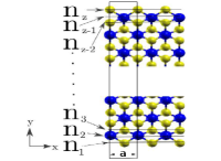
Rectangular supercells were build for the zigzag and armchair nanoribbons, periodic in the direction, with lattice parameters of =3.51 and =6.08 Å respectively. To simulate isolated ribbons, the inplane and perpendicular distances between ribbons in adjacent supercells have to be larger than 10Å. In the case of ribbons, the cell optimizations were just in the x-direction. The Brillouin zones of the GNR unit cells are sampled by Monkhorst-Pack43 grids of the form , in the 2D structures and for the 1D structures.
Depending on their width, ribbons present different edge terminations, defining ribbon’s families. Six possible edge terminations are found for the zigzag ribbons and two for the armchair, therefore here we studied 6 zigzag families and 2 armchair families. All ribbons were also hydrogen passivated.
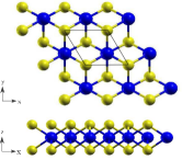
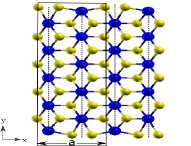
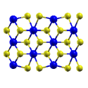
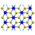
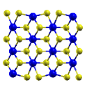
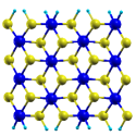
11(a) shows the structure in the and views of the T configuration. We classified the zigzag terminations according to the three bottom atomic lines and the three top atomic lines ( 1(b)). The ribbon that starts with three atoms lines (-direction as reference) and ends with three atoms lines is called – ribbon, where ,, , , , could be Se or Ni, is the total number of rows in the nanorribon. Zigzag ribbons have the restriction that and occurs in the cyclic order NiSeSe due to the periodicity. The six representative zigzag edge terminations are shown in (2).
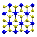
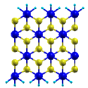
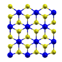
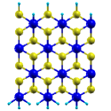
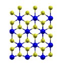
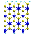
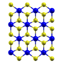
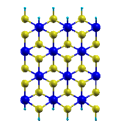
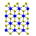
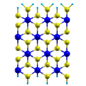
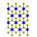
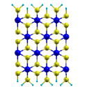
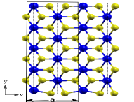
In the case of armchair nanoribbons two representative families appear; we call them Ni-aligned-Ni (Fig. 1(c)) and Ni-centered-Se (Fig. 1(d)). We chose this nomenclature according to the atomic symmetry of the opposite edges as shown by the dotted lines in the lower panels of 1.
Eight root ribbons were build as case studies to characterize the edge structure and electronic properties of each family; 6 for the zigzag families and 2 for the armchair families (2 and 3 respectively). Throughout this work we will mainly work with these 8 ribbons.
After structure relaxation of the root ribbons, their electronic properties were investigated. All root nanoribbons were hydrogen passivated to satisfy the surface dangling bonds. The hydrogen passivated ribbons were also relaxed and their electronic properties were also investigated. The semiconductor ribbons are expanded to 35 Å in order to find the variation of the electronic band gap with the ribbon’s width.
3 Results and discussion
3.1 Structure and stability
The 2D-NiSe2 sheets were built and geometry optimized in the T and H configurations with a total energy for the T-structure 0.45 eV lower than for the metastable H structure. In the T-structure the Ni-Se and Se-Se interatomic distances were 2.39 and 3.25 Å respectively with a band gap of 0.11 eV. Metastable H-NiSe2 presents Ni-Se and Se-Se interatomic distances of 2.41 and 2.63 Å respectively, with a metallic behavior. Phonon modes for both structures were calculated in order to guarantee the stability. Any negative frequency was found in both cases, an indication of the stability for both structures. All these results are in good agreement with those reported by Ataca et al.14, validating our calculations and the starting system from where to build our nanoribbons.
The cohesive energy of T and H systems relative to free constituent atoms was calculated as , in terms of the total energy of NiSe2, ET[NiSe2], and total energies of free Ni and Se atoms, ET[Ni] and ET[Se], respectively. The cohesive energies are 12.51 eV and 12.06 eV for T and H structures respectively; indicating a strong cohesion relative to free atoms of the constituents.
A high cohesion energy is important and required for stability of the compound, but more important for the synthesis is the formation energy () with respect to bulk systems, calculated with the expression
Natural references for the formation energy of this compound are the corresponding Ni and Se. The formation energy for T- and H-NiSe2 systems are 0.81 and 0.36 eV respectively; the higher the value, the more stable the system.
Formation energies were also calculated with the experimental values of cohesive energies from Kittel et al. 44 as 3.20 and 2.74 eV for T and H, respectively. Both ’s are positive, implying that T-NiSe2 and H-NiSe2 are stable and metastable respectively, as previously reported in by Ataca et al. 14.
We built our root nanoribbons by cutting them from a 2D sheet of the relaxed T-2D-NiSe2 2D sheet in the zigzag and armchair directions (2 and 3).
Their and energies were calculated using the expressions and , with , and the number of Ni, Se and H atoms; only for H passivated ribbons. For the of hydrogen terminated ribbons, we use our calculated binding energy for H2 of 3.25 eV/atom.
Bare ribbons present positive ranging from 3.92-4.07 eV/atom, which indicates strong cohesion relative to the constituents free atoms (1). The three bare root systems with lower cohesive energies are NiSeSe-NiSeSe, SeNiSe–NiSeSe and SeNiSe–NiSeSe, all characterized by two consecutive lines of semiconductor atoms at one or both of the edges. 1 also includes the per atom for all bare ribbons. Bare SeNiSe–SeNiSe, SeNiSe–NiSeSe and Ni-centered-Se nanoribbons present an with values between the range of the T- and H-2D structures.
| Cohesive energy | Formation energy | |||
|---|---|---|---|---|
| Ribbon name | per atom (eV) | per atom (meV) | ||
| Bare | Passivated | Bare | Passivated | |
| T-NiSe2 | 4.17 | – | 270.0 | – |
| H-NiSe2 | 4.02 | – | 120.0 | – |
| NiSeSe–SeSeNi | 4.07 | 5.90 | 24.5 | -93.7 |
| NiSeSe–SeNiSe | 4.06 | 5.48 | 94.2 | 37.0 |
| NiSeSe–NiSeSe | 3.97 | 5.59 | 78.1 | 67.1 |
| SeNiSe–SeNiSe | 4.05 | 5.13 | 152.0 | 147.8 |
| SeNiSe–NiSeSe | 4.00 | 5.21 | 154.1 | 121.3 |
| SeSeNi–NiSeSe | 3.92 | 5.28 | 119.4 | 101.3 |
| Ni-aligned-Ni | 4.01 | 5.69 | 107.2 | 60.6 |
| Ni-centered-Se | 4.04 | 5.44 | 135.4 | 101.2 |
Relaxation of the armchair ribbon edges results in an increment of the edge Ni-Se distance in 1.67 % with respect the bulk Ni-Se distance, while the edge Se-Ni-Se angle is reduced in 24%.
As mentioned before, all root ribbons were hydrogen passivated. In the T-NiSe2 2D structure, each Ni atom is bonded to 6 Se atoms and each Se atom is bonded to 3 Ni atoms. In contrast, ribbons edges present dangling bonds that were satisfied with hydrogens for passivation. We call natural passivation the one shown in 2 and 3 for zigzag and armchair ribbons, with a hydrogen atom added to the system to complete the 6 and 3 bonds for each Se or Ni edge atoms.
After H passivation and geometry relaxation of the ribbons, H-Se and H-Ni distances are 1.49 Å and 1.47 Å respectively.
3.2 Electronic Properties
Band structures of all root systems were obtained with the same results for spin polarized and non-spin-polarized calculations, which indicates that the systems are non-magnetic in all cases; i.e. all the structures present perfect spin degeneration.
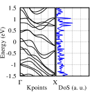
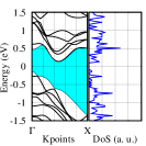
We find that all root zigzag bare-terminated nanoribbons are metallic. After natural hydrogen passivation, only two of them have an energy band gap, the SeNiSe–SeNiSe and SeNiSe–NiSeSe. Contrary to the results in zigzag MoS2 nanoribbons23, where bare and hydrogenated zigzag nanoribbons were metallic. The main difference between MoS2 zigzag nanoribbons and our systems is the base 2D structure metal-chalcogenide. In zigzag nanoribbons based on H-like, there is no possibility that two consecutive chalcogenide atomic lines can exist at the same edge. While in zigzag nanoribons based on T-like structures, it is possible to have two consecutive chalcogenide (Se) atomic lines, even more, the geometry allows to have the last line of atoms in both edges composed of chalcogenides with one and two edge lines of Se atoms.
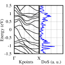
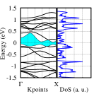
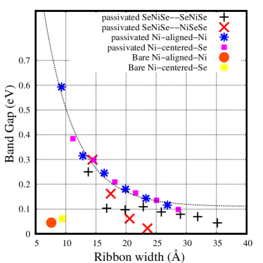
Zigzag nanoribbons are divided in two groups: those with an outermost Ni atomic line (NiSeSe–SeSeNi, NiSeSe–SeNiSe and NiSeSe–NiSeSe, figures 22(a), 2(c) and 2(e) and their corresponding H passivations: 22(b), 2(d) and 2(f)), and those with all outermost Se atomic lines (SeNiSe–SeNiSe, SeNiSe–NiSeSe and SeSeNi–NiSeSe, figures 22(g),2(i) and 2(k) and their corresponding passivations: 22(h),2(j) and 2(l)). Surprisingly all bare and hydrogen passivated zigzag nanoribbons of the former group were metals, unlike the common finding that semiconductor nanostructures always have a larger band gap than their 2D values 45. Recent studies 18, 19 show that centered honeycomb nanostructures enhance electrocatalytic activity due to the high concentration of metallic edges, this suggest that, NiSeSe–SeSeNi will be the best candidate as catalyst for hydrogen evolution, but also NiSeSe–SeNiSe and NiSeSe–NiSeSe will be used for the same process. In the latter group, two of the H passivated root ribbons are semiconductors (i.e. the natural H passivated SeNiSe–SeNiSe and SeNiSe–NiSeSe ribbons). The variation ribbon’s width versus the band gap value is shown in 4. According to 1, the stablest zigag ribbon is the SeNiSe–SeNiSe, which is found to have a semiconductor behavior for all calculated widths ( 4). In contrast, we found that, as the width of the SeNiSe–NiSeSe ribbon increases, the system presents a semiconductor-metal transition at 23.55 Å.
We also explored other possible edge hydrogen passivation densities for all root zigzag ribbons. The hydrogen binding energy () was used as an indicator of higher or lower stability, see 2. For example: NiSeSe–SeSeNi was hydrogen passivated with 3 (i. e. the natural full passivation of the dangling bonds), 2 and 1 hydrogens per edge Ni atom (H6, H3, and H2). In the case of the NiSeSe–SeNiSe ribbon, one edge was fixed with one hydrogen attached to the outermost Se atom and one hydrogen to its neighboring Ni atom, while on the other edge, the hydrogenation varied from 3, 2 and 1 H for the edge Ni atom (H5, H4, and H3). For the NiSeSe–NiSeSe ribbon, four hydrogenations were studied; one, where all dangling bonds are satisfied (the so called natural hydrogenation with 6 H in total, H6), two, where one hydrogen is attached to the outermost Se edge atoms (H5), three, where one H atom is attached to the outermost Se edge atom and two to the outermost Ni edge atom (H4), and four, where the outermost Se and Ni edge atom in opposited edges are only passivated with one hydrogen each one (H3).
The natural hydrogenation for the SeNiSe–SeNiSe ribbon is the following: Ni atoms and outermost Se atoms were passivated with one hydrogen p/atom, satisfying the dangling bonds. Alternative passivations were: 1. Remove the H passivation of the Ni atoms, leaving it with one dangling bond (H2-Se). 2. Removing the H passivation of the Se atom, leaving it with one dangling bond (H2-Ni). The latter case of the unpassivated Se atom is a clear example of a non stable system with 2.78 eV, which is almost 0.5 eV below the energy for H2, turning the electronic properties of the fully passivated semiconductor ribbon to a metallic behavior. This means that in presence of H2 any ribbon with edge Se atoms should always be H passivated.
In ribbons with two consecutive atomic rows of Se at any of the two edges, the natural passivation includes two hydrogens attached to the outermost Se atoms and one hydrogen attached to the neighbor Se atom. The SeNiSe–NiSeSe ribbon was passivated with two (H5) and one (H4) H in the outer Se for the consecutive Se rows, while the others Se remained with one bonded hydrogen atom. Similarly, the SeSeNi–NiSeSe ribbon was passivated with two (H6) and one (H4) hydrogen atoms in the outer Se for the consecutive Se rows.
Metallic ribbons from the SeSeNi–NiSeSe family were build with widths from 17.08 to 33.17 Å, with all the outer Se atoms passivated with two hydrogens, i. e. fully satisfying the dangling bonds. In some cases, relaxation of these ribbons resulted in the separation of SeH2 molecules from both edges, and a final configuration of a SeNiSe–SeNiSe ribbon. This is a strong suggestion that if ribbons are experimentally formed by cutting 2D T-NiSe2, ribbons from the SeNiSe–SeNiSe family are much more probable to be found than those from the SeSeNi–NiSeSe family. Also, during experiments SeH2 molecules are prone to desorb from the ribbon’s edges.
| Average binding energy of hydrogen (eV) | ||||
| H6 | H4 | H2 | ||
| NiSeSe–SeNiSe | 3.05 | 3.09 | 3.06 | |
| H5 | H4 | H3 | ||
| NiSeSe–SeNiSe | 3.12 | 3.15 | 3.18 | |
| H6 | H5 | H4 | H3 | |
| NiSeSe–NiSeSe | 3.23 | 3.34 | 3.38 | 3.30 |
| H4 | H2-Ni | H2-Se | ||
| SeNiSe–SeNiSe | 3.24 | 2.78 | 3.47 | |
| H5 | H4 | |||
| SeNiSe–NiSeSe | 3.16 | 3.26 | ||
| H6 | H4 | |||
| SeSeNi–NiSeSe | 3.21 | 3.42 | ||
Several of the s are higher than the in H2, and in general the energy increases as the density decreases.
It is worth mentioning that all metallic systems remained metallic and the two semiconductors became metallic when reducing the hydrogenation densities.
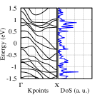
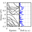
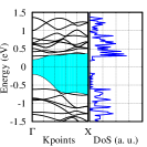
Our root armchair bare-termination nanoribbons are semiconductors with a very small band gap; 0.045 eV and 0.061 eV for Ni-aligned-Ni and Ni-centered-Se, respectively. Bare terminated armchair ribbons were built with widths from 10 Å to 30 Å and only the root ribbons are semiconductors. In this work, the largest electronic band gap is for hydrogen passivated armchair nanoribbons with gaps of 0.59 and 0.38 eV, for passivated root Ni-aligned-Ni and passivated Ni-centered-Se nanoribbons respectively. In figure 4, the variation of electronic band gap for hydrogen passivated is reported. The tendency of the band gap for the armchair follows the expression , where a= 2.59 eV, 5.33 Å and is the ribbon’s width.
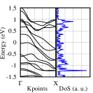
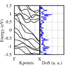
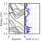
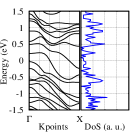
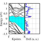
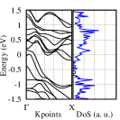
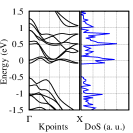
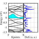
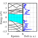
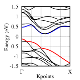
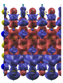
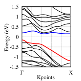
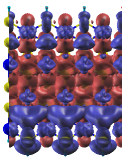
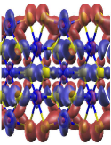
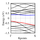
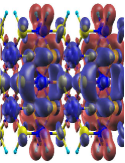
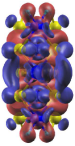
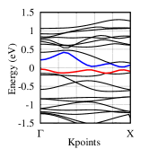
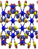
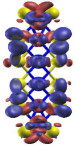
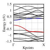
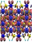
5 shows the band structure of the semiconductor root systems with the highest occupied and the lowest unoccupied bands highlighted in red and blue respectively. The highest occupied and lowest unoccupied orbitals are also illustrated in the figure with the same color code. The SeNiSe–SeNiSe root ribbon presents a symmetrical distribution of both orbitals with respect of the axis. In contrast the SeNiSe–NiSeSe system present an accumulation of the top valence orbital on the ribbon’s bottom SeNiSe edge while the bottom conduction orbital localizes on the ribbon’s top NiSeSe edge. Both systems are indirect semiconductors.
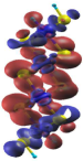
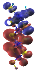
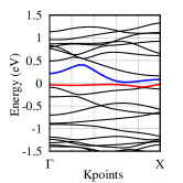
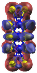
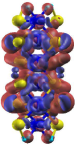
Regarding the armchair ribbons, the band structure and highest occupied and lowest unoccupied orbitals are also shown. In this case all the ribbons present symmetry of the orbitals with respect of the axis and the band gaps are also indirects.
4 Summary
This work pioneers the ab-initio studies of centered honeycomb nanoribbons, defining the representative ribbon’s families and opening the filed to study other systems in the T structure. In this work, we use first principles calculations to explore the different atomic arrangements for NiSe2 nanoribbons in the stable T crystalline structure. Zigzag bare-nanoribbons geometrical reconstruction leads to metallic systems, while just two hydrogen passivated nanoribbons are semiconductors. NiSeSe–SeSeNi has the largest metallic edge, suggesting that this ribbon will be the perfect candidate as catalyst for hydrogen evolution. SeNiSe–SeNiSe is the stablest zigzag nanoribon. Studies of edge H passivation densities reveals that SeSeNi- edges are prone to convert to SeNiSe by a SeH2 desorption mechanism. Only thin bare-armchair nanoribbon are semiconductors with a very small band gap (0.045 and 0.061 eV), thicker ones are metals. When armchair ribbons are hydrogen passivated, the band gaps increase considerably to values up to 0.6 eV. The study of the variation in electronic band gap with the width was done and we report the asymptotic tendency to T-NiSe2 band gap (0.11 eV) for armchair passivated nanoribbons.
The authors thank DGTIC-UNAM. JARR acknowledges support from DGAPA-UNAM. GGN acknowledges support from DGAPA-UNAM project number 102513. This work was done under the support of FICSAC with the program: Atraction of visiting academics 2012 and by the Physics and Mathematics Department of UIA.
References
- Lebègue and Eriksson 2009 Lebègue, S.; Eriksson, O. Phys. Rev. B 2009, 79, 115409
- Novoselov et al. 2005 Novoselov, K. S.; Jiang, D.; Schedin, F.; Booth, T. J.; Khotkevich, V. V.; Morozov, S. V.; Geim, A. K. Proc. Natl. Acad. Sci. USA 2005, 102, 10451–10453
- Novoselov et al. 2004 Novoselov, K. S.; Geim, A. K.; Morozov, S. V.; Jiang, D.; Zhang, Y.; Dubonos, S. V.; Grigorieva, I. V.; Firsov, A. A. Science 2004, 306, 666–669
- Britnell et al. 2012 Britnell, L.; Gorbachev, R.; Jalil, R.; Belle, B.; Schedin, F.; Mishchenko, A.; Georgiou, T.; Katsnelson, M.; Eaves, L.; Morozov, S.; Peres, N.; Leist, J.; Geim, A.; Novoselov, K.; Ponomarenko, L. Science 2012, 335, 947–950
- Vogt et al. 2012 Vogt, P.; De Padova, P.; Quaresima, C.; Avila, J.; Frantzeskakis, E.; Asensio, M. C.; Resta, A.; Ealet, B.; Le Lay, G. Phys. Rev. Lett. 2012, 108, 155501
- Dean et al. 2010 Dean, C. R.; Young, A. F.; Meric, I.; Lee, C.; Wang, L.; Sorgenfrei, S.; Watanabe, K.; Taniguchi, T.; Kim, P.; K. L Shepard, J. H. Nature Nanotechnology 2010, 5, 722–726
- Osada and Sasaki 2009 Osada, M.; Sasaki, T. J. Mater. Chem. 2009, 19, 2503–2511
- Li et al. 2009 Li, X.; Cai, W.; An, J.; Kim, S.; Nah, J.; Yang, D.; Piner, R.; Velamakanni, A.; Jung, I.; Tutuc, E.; Banerjee, S. K.; Colombo, L.; Ruoff, R. S. Science 2009, 324, 1312–1314
- Lee et al. 2012 Lee, Y.-H.; Zhang, X.-Q.; Zhang, W.; Chang, M.-T.; Lin, C.-T.; Chang, K.-D.; Yu, Y.-C.; Wang, J. T.-W.; Chang, C.-S.; Li, L.-J.; Lin, T.-W. Advanced Materials 2012, 24, 2320–2325
- Coleman et al. 2011 Coleman, J. N. et al. Science 2011, 331, 568–571
- Nicolosi et al. 2013 Nicolosi, V.; Chhowalla, M.; Kanatzidis, M. G.; Strano, M. S.; Coleman, J. N. Science 2013, 340, 1226419
- Wilson and AD 1969 Wilson, J.; AD, Y. Adv. in Phys. 1969, 18, 193–335
- Mattheiss 1973 Mattheiss, L. F. Phys. Rev. B 1973, 8, 3719–3740
- Ataca et al. 2012 Ataca, C.; Sahin, H.; Ciraci, S. The Journal of Physical Chemistry C 2012, 116, 8983–8999
- Mak et al. 2010 Mak, K. F.; Lee, C.; Hone, J.; Shan, J.; Heinz, T. F. Phys. Rev. Lett. 2010, 105, 136805
- Tongay et al. 2012 Tongay, S.; Zhou, J.; Ataca, C.; Lo, K.; Matthews, T. S.; Li, J.; Grossman, J. C.; Wu, J. Nano Letters 2012, 12, 5576–5580
- Sundaram et al. 2013 Sundaram, R. S.; Engel, M.; Lombardo, A.; Krupke, R.; Ferrari, A. C.; Avouris, P.; Steiner, M. Nano Letters 2013, 13, 1416–1421
- Lukowski et al. 2013 Lukowski, M.; Daniel, A.; Meng, F.; Forticaux, A.; Li, L.; Jin, S. J. Am. Chem. Soc. 2013, published online, doi:10.1021/ja404523s
- Voiry et al. 2013 Voiry, D.; Yamaguchi, H.; Li, J.; Silva, R.; Alves, D.; Fujita, T.; Chen, M.; Asefa, T.; Shenoy, V.; Eda, G.; Chhowalla, M. Nat. Mater. 2013, published online, doi: 10.1038/nmat3700
- Han et al. 2007 Han, M. Y.; Özyilmaz, B.; Zhang, Y.; Kim, P. Phys. Rev. Lett. 2007, 98, 206805
- Son et al. 2006 Son, Y.-W.; Cohen, M. L.; Louie, S. G. Phys. Rev. Lett. 2006, 97, 216803
- Nakada et al. 1996 Nakada, K.; Fujita, M.; Dresselhaus, G.; Dresselhaus, M. S. Phys. Rev. B 1996, 54, 17954–17961
- Botello-Méndez et al. 2009 Botello-Méndez, A. R.; López-Urías, F.; Terrones, M.; Terrones, H. Nanotechnology 2009, 20, 325703
- Yue et al. 2012 Yue, Q.; Chang, S.; Kang, J.; Zhang, X.; Shao, Z.; Qin, S.; Li, J. Journal of Physics: Condensed Matter 2012, 24, 335501
- Hromadová et al. 2013 Hromadová, L.; Martonak, R.; Tosatti, E. Phys. Rev. B 2013, 87, 144105
- Ataca et al. 2011 Ataca, C.; Sahin, H.; Akturk, E.; Ciraci, S. The Journal of Physical Chemistry C 2011, 115, 3934–3941
- Koski et al. 2012 Koski, K. J.; Wessells, C. D.; Reed, B. W.; Cha, J. J.; Kong, D.; Cui, Y. J. of the American Chemical Society 2012, 134, 13773–13779
- She et al. 2008 She, G.; Zhang, X.; Shi, W.; Cai, Y.; Wang, N.; Liu, P.; Chen, D. Crystal Growth and Design 2008, 8, 1789–1791
- Podberezskaya et al. 2001 Podberezskaya, N.; Magarill, S.; Pervukhina, N.; Borisov, S. Journal of Structural Chemistry 2001, 42, 654–681
- Ding et al. 2011 Ding, Y.; Wang, Y.; Ni, J.; Shi, L.; Shi, S.; Tang, W. Physica B: Condensed Matter 2011, 406, 2254 – 2260
- Yun et al. 2012 Yun, W. S.; Han, S. W.; Hong, S. C.; Kim, I. G.; Lee, J. D. Phys. Rev. B 2012, 85, 033305
- Moloto et al. 2011 Moloto, N.; Moloto, M. J.; Coville, N. J.; Ray, S. S. Journal of Crystal Growth 2011, 324, 41 – 52
- Sobhani et al. 2012 Sobhani, A.; Salavati-Niasari, M.; Davar, F. Polyhedron 2012, 31, 210 – 216
- Hankare et al. 2010 Hankare, P.; Jadhav, B.; Garadkar, K.; Chate, P.; Mulla, I.; Delekar, S. Journal of Alloys and Compounds 2010, 490, 228 – 231
- Fan et al. 2009 Fan, H.; Zhang, M.; Zhang, X.; Qian, Y. Journal of Crystal Growth 2009, 311, 4530 – 4534
- Zhao et al. 2005 Zhao, A.; Xu, L.; Luo, T.; Qian, Y. Chemistry Letters 2005, 34, 1136–1137
- Giannozzi et al. 2009 Giannozzi, P. et al. Journal of Physics: Condensed Matter 2009, 21, 395502
- License 1991 License, G. G. P. GNU Project 1991
- Vanderbilt 1990 Vanderbilt, D. Phys. Rev. B 1990, 41, 7892–7895
- Rappe et al. 1990 Rappe, A. M.; Rabe, K. M.; Kaxiras, E.; Joannopoulos, J. D. Phys. Rev. B 1990, 41, 1227–1230
- Perdew et al. 1992 Perdew, J. P.; Chevary, J. A.; Vosko, S. H.; Jackson, K. A.; Pederson, M. R.; Singh, D. J.; Fiolhais, C. Phys. Rev. B 1992, 46, 6671–6687
- Perdew et al. 1996 Perdew, J. P.; Burke, K.; Ernzerhof, M. Phys. Rev. Lett. 1996, 77, 3865–3868
- Monkhorst and Pack 1976 Monkhorst, H. J.; Pack, J. D. Phys. Rev. B 1976, 13, 5188–5192
- Kittel and McEuen 2005 Kittel, C.; McEuen, P. Introduction to solid state physics, 8th ed.; Wiley New York, 2005
- Deng et al. 2012 Deng, H.-X.; Li, S.-S.; Li, J.; Wei, S.-H. Phys. Rev. B 2012, 85, 195328