Supplemental information for “Observation of the SU(4) Kondo state in a double quantum dot”
S1 Full LBTP survey
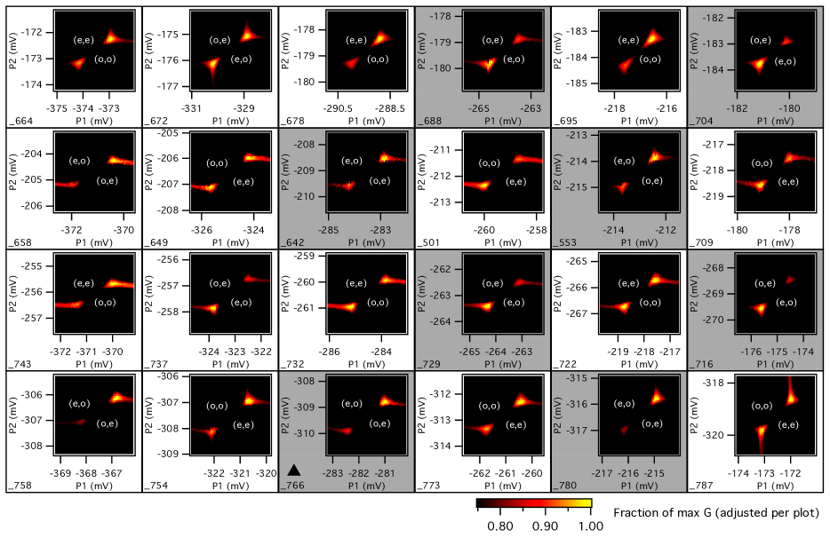
The data presented in Fig. 1b are only a subset of the full survey of conductance around lines between triple points (LBTPs). The full survey, shown in Fig. S1, demonstrates that 11/12 of or LBTPs exhibit higher conductance towards the adjacent (1,1) hexagon. In addition, twelve (1,1)/(2,0) or (0,2)/(1,1) LBTPs were surveyed: these should possess a five-fold degeneracy assuming the (2,0) ground state is a singlet rather than triplet. The and LBTPs differ qualitatively from the (1,1)/(2,0) and (0,2)/(1,1) LBTPs in that the latter class of LBTPs do not exhibit a simple pattern of which end of the LBTP has higher conductance. Experimental parameters , and peak conductances are extracted from each data set and summarized in Table S1.
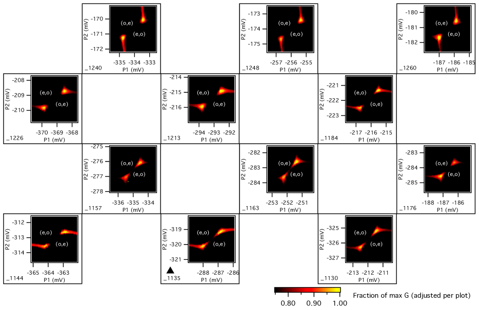
Because we claim that the and LBTP data reflect the particle-hole symmetry of a four-fold degenerate state, it is natural to expect that the pattern is destroyed when the four-fold degeneracy is broken. Fig. S2 shows the and LBTPs surveyed again in an in-plane magnetic field of 2.0 T, corresponding to meV for . Here, , for all of the surveyed LBTPs. With the Zeeman splitting having broken the spin degeneracy at the LBTPs, a periodic pattern is no longer discernible. Table S2 summarizes the extracted parameters for each data set, as in Table S1.
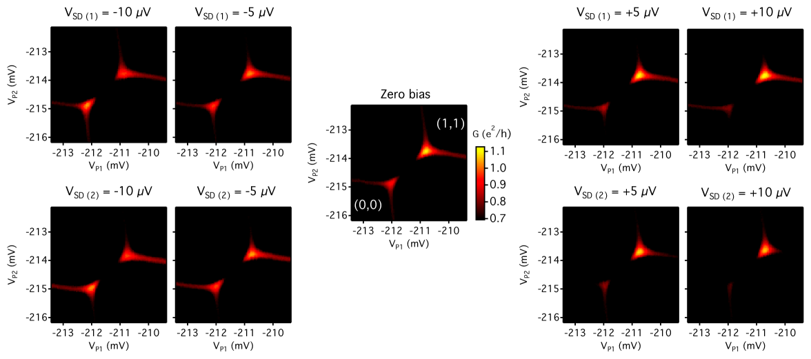
Fig. S3 shows how a small but finite affects the observed asymmetry at an LBTP. The LBTP measured here corresponds to the same absolute electron occupation numbers as data set 553 shown in Fig. S1. Only for negative approaching V does the conductance near (0,0) exceed that near (1,1). For positive , the pattern of higher conductance nearer to (1,1) than (0,0) is actually exaggerated. The effect of finite is similar regardless of whether it is applied to dot 1 or 2. Input offset voltages from current amplifiers could obscure our observed pattern, were it not for our ability to stabilize these voltages to within 1 V (see section S8.1).
| Data set | Data set | ||||||||
|---|---|---|---|---|---|---|---|---|---|
| _664 | 24 | 32 | 0.82 | 0.89 | _743 | 27 | 31 | 0.43 | 0.80 |
| _672 | 29 | 36 | 0.69 | 0.66 | _737 | 27 | 29 | 0.66 | 0.77 |
| _678 | 35 | 39 | 0.63 | 0.68 | _732 | 27 | 31 | 0.56 | 0.78 |
| _688 | 28 | 36 | 0.54 | 0.67 | _729 | 28 | 31 | 0.59 | 0.79 |
| _695 | 32 | 42 | 0.67 | 0.70 | _722 | 30 | 33 | 0.69 | 0.80 |
| _704 | 33 | 32 | 0.73 | 0.78 | _716 | 32 | 34 | 0.74 | 0.80 |
| _658 | 26 | 27 | 0.51 | 0.89 | _758 | 28 | 33 | 0.48 | 0.68 |
| _649 | 30 | 27 | 0.66 | 0.88 | _754 | 30 | 31 | 0.64 | 0.67 |
| _642 | 28 | 27 | 0.75 | 0.90 | _766 | 27 | 30 | 0.51 | 0.64 |
| _501 | 26 | 31 | 0.51 | 0.84 | _773 | 27 | 34 | 0.59 | 0.68 |
| _553 | 28 | 29 | 0.82 | 0.89 | _780 | 29 | 34 | 0.73 | 0.67 |
| _709 | 30 | 33 | 0.74 | 0.92 | _787 | 29 | 34 | 0.77 | 0.66 |
| Data set | ||||
|---|---|---|---|---|
| _1240 | 29 | 33 | 0.98 | 0.70 |
| _1248 | 29 | 34 | 0.88 | 0.65 |
| _1260 | 31 | 36 | 0.90 | 0.80 |
| _1226 | 32 | 32 | 0.62 | 0.78 |
| _1213 | 30 | 35 | 0.70 | 0.83 |
| _1184 | 31 | 32 | 0.76 | 0.87 |
| _1157 | 34 | 32 | 0.94 | 0.95 |
| _1163 | 31 | 35 | 0.94 | 0.99 |
| _1176 | 35 | 31 | 0.88 | 0.98 |
| _1144 | 32 | 29 | 0.58 | 1.02 |
| _1135 | 32 | 31 | 0.75 | 0.99 |
| _1130 | 30 | 35 | 0.79 | 0.97 |
S2 Summary of NRG calculations
S2.1 NRG calculations
In our numerical calculations the double quantum dot (DQD) system is modeled by the following Hamiltonian
| (1) |
where
| (2) | |||||
describes the two dots, with the occupation number operator of dot for spin , the energy of a spin- electron residing on dot . () denotes the intradot (interdot) Coulomb correlations, while is the magnetic field applied along the -direction and is the -component of the double dot’s spin. The tunneling Hamiltonian reads
| (3) |
where is the creation operator of an electron in lead coupled to dot , with momentum and spin of energy . Tunneling processes between the dots and leads are described by hopping matrix elements . Tunneling between the two dots is suppressed by tuning gates in our experiment, and hence is omitted from the model. The leads are described by noninteracting quasiparticles
| (4) |
Due to the coupling to external leads, the dots’ levels acquire a width described by , with the density of states of lead coupled to dot .
We performed the full density-matrix numerical renormalization group calculations (fDM-NRG) [1, 2, 3, 4], employing the Budapest Flexible DM-NRG code [5]. For efficient calculations, we used the charge and the spin symmetries in each channel, resulting in four symmetries altogether. When considering the effect of external magnetic field , the spin invariance is reduced to the symmetry for the spin -component in each channel. In our computations we retained states at each iteration depending on the exploited symmetries and used the discretization parameter .
We calculated the linear conductance through dot using the following formula
| (5) |
where is the Fermi-Dirac distribution function and is the left-right asymmetry factor for dot , with . denotes the spectral function of the -th dot level for spin , , with the Fourier transform of the retarded Green’s function, . To improve the quality of the spectral functions and reduce the effects related with broadening of Dirac delta functions, we also used the z-averaging trick [6].
S2.2 Choosing NRG parameters
Most of the parameters used in NRG calculations may be extracted from routine measurements of the two dots. To a good approximation, a small decrement in the dot level is proportional to a small increment in gate voltage. The proportionality constant, as well as the charging energies , , and , are measured directly by routine bias spectroscopy. may be extracted from the change in of dot 1’s Coulomb blockade peak position as an electron is added to dot 2, or vice versa. and are determined from Coulomb blockade diamonds taken over a wider range of energy; results of the conductance calculations around the LBTP are largely insensitive to values of and as they are much greater than .
and define the coupling strength (or linewidth) for dot 1 and 2 in an underlying Anderson model. may be extracted by taking cuts away from the LBTP on a mixed valence peak of dot 1 (side of charge stability hexagon). There, for large intradot interactions and , the FWHM of the conductance curve , divided by T, must be a universal function of , and likewise for dot 2. In principle, for an experimentally measured at known temperature , should be specified by NRG calculations of that universal function. In practice, however, the parameters may require some fine tuning of order 10% for best agreement, as other effects may affect the widths of the measured peaks (perhaps Fano interference at zero magnetic field, or neglected internal states of the dots, etc.).
Effectively, the NRG calculations use two free parameters, the asymmetry parameters and . These are selected such that the calculations reproduce the experimentally observed height of the mixed valence peaks of dot 1 and 2, as well as the temperature dependent conductance in other regions of parameter space.
In Fig. 4, most of the parameters used for the spectral function calculation were unchanged from those used in NRG calculations earlier in the paper. However, in the calculation we set for simplicity, as it would only contribute a scale factor otherwise. For each value of , the corresponding values of and are shown in Table S4.
For computational convenience we treated an LBTP. However, by means of a particle-hole transformation (, , , ), we use these calculations to describe the LBTP. The spectral functions shown in Fig. 4 are the result of this particle-hole transformation. For this data set, the precise values of and were not determined, as the tuning of the device was different from when the data for Figs. 2 and 3 were taken. Nonetheless, the values should be similar and the spectral functions describe the data remarkably well.
S3 Extracting LBTP cuts from 2D data sets
The zero-detuning cuts presented in Fig. 2c and 2d were extracted numerically from 2D data sets. The cuts are highly sensitive to cut direction such that adjusting the endpoints by even a few eV can result in significantly different conductances along the cut. With experimental data alone, this poses a significant problem, since the line of zero detuning cannot be exactly identified. Moreover, it is difficult to control for shifts of the LBTP unrelated to renormalization as the temperature is varied. Physically meaningful shifts of the mixed-valence peaks with temperature are to be expected, but undesirable shifts, predominantly from random charge transitions in the donor layer of the heterostructure, may also contribute.
To address these concerns, for fixed NRG parameters we compare the 2D experimental data sets to the 2D NRG calculations, at each measured temperature. The pseudospin-resolved conductances from the experimental data and from NRG were fit to Lorentzians to find the peak positions. The experimental data were then offset such that the peak positions matched those in the NRG data. Some manual shifts of 0.005 meV or less were used following the fitting procedure to provide best agreement along the LBTP cuts. Note that the scale factor between gate voltage and energy is experimentally determined, and only the offsets of the axes are adjusted.
S4 Temperature dependence details
As stated in the main text, the point = -0.03 meV was chosen for the temperature dependence because it is a point where is large compared to experimentally accessible temperatures. However, apart from the saturation observed at 40 mK that prevents observation of the low-T rollover, the experimental data are consistent with both SU(4) universal scaling and NRG calculations for our device configuration at other points along the LBTP. In Figs. S4 and S5 we show the temperature dependence at = -0.04 meV and = -0.05 meV, respectively.
Uncertainties in the experimental conductances of Fig. 3 are likely dominated by the uncertainty in maintaining constant and between data taken at different temperatures, rather than conductance noise. We extract the conductances from the 2D maps of Figs. 2a and 2b and similar maps at other temperatures. The offsets (but not the scale) of the and experimental axes of Figs. 2a and 2b are set using the theoretical calculations, and this considerably reduces this uncertainty. After this alignment procedure, the remaining uncertainty in and may be conservatively taken as the pixel spacing of and in our 2D conductance maps, approximately 0.003 meV.
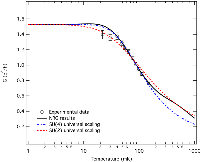
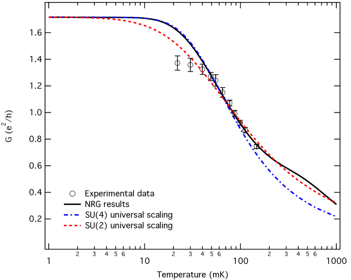
In determining error bars, experimental points in the 2D conductance map neighboring meV are considered to be independent measurements of the conductance at meV, with a Gaussian weight: , where meV. The error bars then reflect the standard deviation of the weighted mean, and are largest at low temperatures where the conductance varies the most rapidly in any direction in and . The (unbiased) standard deviation of the weighted mean, , is given by:
| (6) |
where is the weighted mean, , and .
S5 Empirical Kondo forms
The empirical Kondo form was introduced by D. Goldhaber-Gordon, et al. [7] and provides a convenient approximation of conductance through a quantum dot in the SU(2) crossover regime as a function of temperature:
| (7) |
where , , is the conductance attained at zero temperature, and is the Kondo temperature. This form is purely phenomenological and was invented to describe succinctly the numerically-calculated spin-1/2 SU(2) universal scaling [8]. With such a formula it is convenient to estimate from experimental results using nonlinear regression, however care must be taken in its application. Importantly, for and this formula does not describe the universal SU(4) scaling. Various papers have nonetheless used the empirical SU(2) form (7) to fit data for which the applicability is not clear. In the absence of an alternative, this is a reasonable heuristic since the differences between the SU(4) and SU(2) scaling are subtle, but this procedure is not strictly justified.
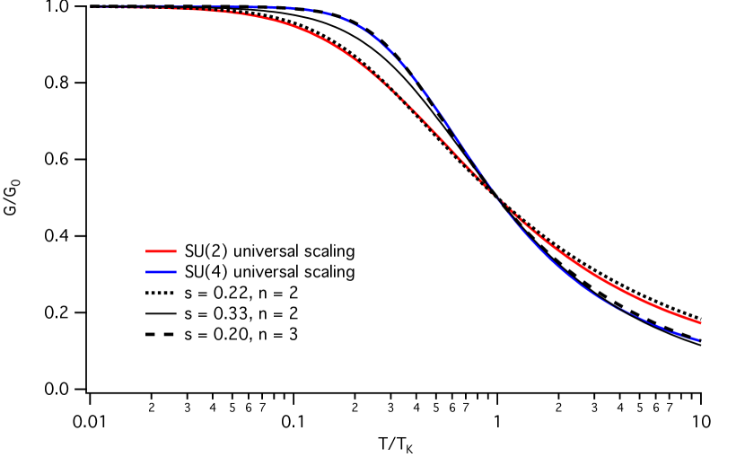
In particular, the leading-order temperature dependence of (7) is quadratic by design at in order to describe SU(2) Kondo scaling, but conformal field theory predicts the SU(4) Kondo state to have a leading-order cubic temperature dependence at , despite retaining a Fermi liquid character (normally associated with quadratic dependence) [9]. Therefore, both parameters and must be changed to expect a nice agreement for , where the empirical form is designed to apply. Fig. S6 shows how , describes SU(2) universal scaling in the crossover regime. Changing alone is seen to be insufficient to describe the SU(4) universal scaling especially for temperatures , where the fitting is most sensitive. However, a good fit to the SU(4) universal scaling may be obtained with , . We must emphasize that although (7) provides an accurate fitting in the full crossover region, it fails at temperatures , where it does not reproduce the well-known logarithmic behavior characteristic of the Kondo problem.
From our experiences with analyzing the experimental data in this paper, empirical forms must be used with great care and supported by other methods. A blind application to our data would yield spurious conclusions, owing to the saturation at mK. Also, as can be seen from the NRG results for our device, there are some expected deviations from the universal scaling, particularly at , where the empirical forms become less accurate.
S6 -factor calibration
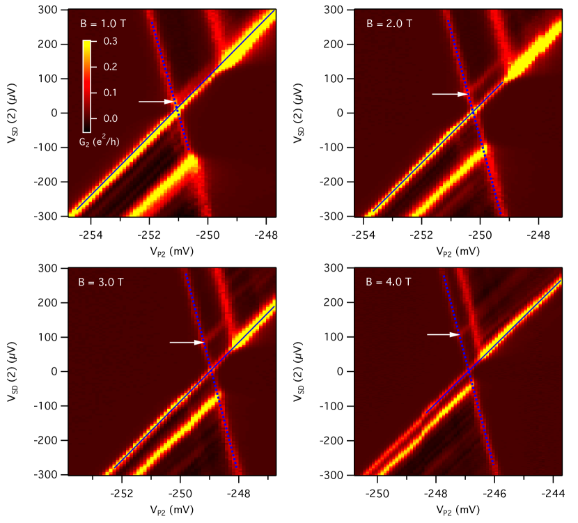
The Zeeman energy is related to the magnetic field by , where is the Bohr magneton and g is the g-factor. Among GaAs/AlGaAs heterostructures, the g-factor can vary considerably, and so we calibrate in situ for our device by looking for a Zeeman splitting in the bias spectroscopy as we vary an in-plane magnetic field. Fig. S7 displays conductance through dot 2, demonstrating the Zeeman splitting. A splitting is seen to emerge by T, though the exact splitting is not resolved owing to the width of the level. As the field is increased, we can extract the splitting by reading off the value of above which the source-drain voltage drop is large enough to allow for inelastic spin flip scattering processes. From this value, any offset for true zero bias is then subtracted (usually a few V or less). Table S3 summarizes the extracted splittings and corresponding g-factors. We find consistent with that of bare GaAs, , and take this value in calculating for given .
| Magnetic field (T) | Splitting (eV) | |
|---|---|---|
| 1.0 | — | — |
| 2.0 | 51 | 0.44 |
| 3.0 | 80 | 0.46 |
| 4.0 | 104 | 0.45 |
S7 Bias spectroscopy at LBTP
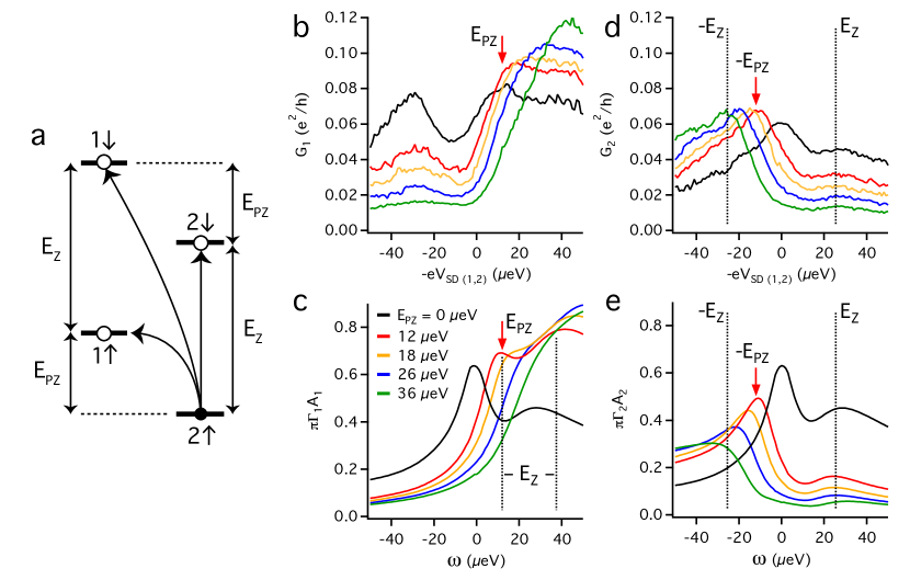
Fig. S8 shows the orbital state-resolved bias spectroscopy and calculated spectral functions at an LBTP, in a 1.0 T Zeeman field. The spectral functions shown are the same as those shown in Fig. 4, up to the particle-hole transformation that was applied to describe the LBTP. By considering the cartoon of Fig. S8a, and identifying each electron-like process with a corresponding hole-like process in Fig. 4a, the relationship between the LBTP and LBTP becomes clearer. We again consider and as equivalent.
In dot 2, all of the expected features are observed (Fig. S8d): a weak peak at , a peak (threshold) that tracks with for , and a purely orbital Kondo peak at for . The overall shapes of the curves are in rough qualitative agreement with the spectral functions in Fig. S8e, although the relative peak heights may differ.
| (meV) | (meV) | (meV) |
|---|---|---|
| 0 | -0.06333 | -0.06167 |
| 0.012 | -0.05667 | -0.06833 |
| 0.018 | -0.05387 | -0.07113 |
| 0.026 | -0.04966 | -0.07534 |
| 0.036 | -0.0445 | -0.0805 |
However, in dot 1 (Fig. S8b), the purely orbital Kondo peak at for is obscured by poorly understood background conductance at positive . Additionally, an unexpected feature is observed at V that does not track with . It is tempting to suggest that the LBTP being measured is actually a (1,1)/(2,0) LBTP. In this interpretation, both dots could hold an unpaired electron, and both dots should exhibit a peak at . In other words, the spectral functions for both dots should look similar to Fig. S8e, with for dot 1. However, the increasing conductance at positive in Fig. S8b is in qualitative agreement with Fig. S8c, and would not be expected in this alternate explanation. Additionally, our ability to maintain electron occupation number assignments is supported by Fig. S1. Therefore, the unexpected feature is instead likely associated with a low-lying excited state.
S8 Technical details
S8.1 Electronics
For the data taken in Fig. 1b and 4 of the paper, custom current amplifiers designed by Y. Chung of Pusan National University (early version of that which is presented in [10]) were used in place of commercial Ithaco / DL Instruments 1211 current amplifiers, which have been previously employed in our measurement setup [11]. The custom amplifiers are crucial to this experiment in that the input offset voltage of the current amplifiers must remain stable over a period of days to avoid applying an uncontrolled source-drain bias across the dot. Over a continuous interval of 2.8 days, the standard deviation of the input offset voltage was measured to be 1.0 V for the amplifier attached to dot 1, and 0.6 V for the amplifier attached to dot 2. The amplifiers were characterized in the same locations where they were used for measurement, as no active temperature control of the amplifiers was performed during measurement or characterization.
S8.2 Magnetic field calibration
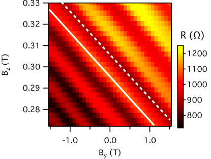
Because of small but uncontrolled sample tilt with respect to axes defined by the two-axis magnet in our experimental dewar, energizing only the in-plane coil will give rise to a perpendicular component as seen by the sample, and vice versa. To apply a magnetic field precisely in the plane of the sample, as is done in Fig. 4, we calibrate in situ using a four-wire current-biased measurement of Shubnikov-de Haas oscillations in resistance, as a function of both the nominally perpendicular field and nominally in-plane magnetic field .
Fig. S9 shows the Shubnikov-de Haas oscillations observed near a perpendicular magnetic field of 0.3 T, and how they track with an added in-plane field. The geometry of the 2DEG mesa is not well defined, so both even and odd components of magnetoresistance contribute to the measured resistance. The observed stripes correspond to a constant perpendicular field. The slope of the stripes gives a compensation factor such that any perpendicular component introduced by the in-plane magnetic field may be cancelled out by application of an added perpendicular field to within a few percent.
Even an applied field in the plane of the sample will subtly modify orbital states because of the finite extent of the electronic wavefunctions normal to the plane, an effect we neglect in our analysis.
S8.3 Bias spectroscopy
To apply and maintain a particular while changing the applied source-drain biases across dot 1 (2) requires some care. Gates P1 and P2 as well as leads S1 and S2 all have capacitances to both dot 1 and dot 2. These capacitances must all be characterized every time the W gates or magnetic field are changed. Once the capacitances are known, electrostatic gating of the dots by the biased source leads may be compensated by changes in and . Further details have been published previously [12].
References
- [1] Wilson, K. G. The renormalization group: Critical phenomena and the Kondo problem. Rev. Mod. Phys. 47, 773–840 (1975).
- [2] Bulla, R., Costi, T. A. & Pruschke, T. Numerical renormalization group method for quantum impurity systems. Rev. Mod. Phys. 80, 395–450 (2008).
- [3] Weichselbaum, A. & von Delft, J. Sum-Rule Conserving Spectral Functions from the Numerical Renormalization Group. Phys. Rev. Lett. 99, 076402 (2007).
- [4] Tóth, A. I., Moca, C. P., Legeza, Ö. & Zaránd, G. Density matrix numerical renormalization group for non-Abelian symmetries. Phys. Rev. B 78, 245109 (2008).
- [5] We used an open-access Budapest NRG code, http://www.phy.bme.hu/~dmnrg/; Legeza, O., Moca, C. P., Tóth, A. I., Weymann, I. & Zaránd, G. arXiv:0809.3143 (2008) (unpublished).
- [6] Oliveira, W. C. & Oliveira, L. N. Generalized numerical renormalization-group method to calculate the thermodynamical properties of impurities in metals. Phys. Rev. B 49, 11986–94 (1994).
- [7] Goldhaber-Gordon, D. et al. From the Kondo Regime to the Mixed-Valence Regime in a Single-Electron Transistor. Phys. Rev. Lett. 81, 5225–8 (1998).
- [8] Costi, T. A., Hewson, A.C. & Zlatic, V. Transport coefficients of the Anderson model via the numerical renormalization group. J. Phys: Cond. Matt. 6, 2519–58 (1994).
- [9] Le Hur, K., Simon, P. & Loss, D. Transport through a quantum dot with SU(4) Kondo entanglement. Phys. Rev. B 75, 035332 (2007).
- [10] Kretinin, A. V. & Chung, Y. Wide-band current preamplifier for conductance measurements with large input capacitance. Rev. Sci. Instrum. 83, 084704 (2012).
- [11] Potok, Ron M. Probing many body effects in semiconductor nanostructures. Ph. D. dissertation. Dept. of Physics, Harvard University (2006).
- [12] Amasha, S. et al. Pseudospin-Resolved Transport Spectroscopy of the Kondo Effect in a Double Quantum Dot. Phys. Rev. Lett. 110, 046604 (2013).