Studies of single-photoelectron response and of performance in magnetic field of a H8500C-03 photomultiplier tube
Abstract
We studied the single-photoelectron detection capabilities of a multianode photomultiplier tube H8500C-03 and its performance in high magnetic field. Our results show that the device can readily resolve signals at the single photoelectron level making it suitable for photon detection in both threshold and ring imaging Cerenkov detectors. We also found that a large longitudinal magnetic field, up to 300 Gauss, induces a change in the relative output of at most 55% for an edge pixel, and of at most 15% for a central pixel. The H8500C-03 signal loss in transverse magnetic fields it is significantly more pronounced than for the longitudinal case. Our studies of single photoelectron reduction in magnetic fields point to the field induced misfocusing of the photoelectron extracted from the photocathode as primary cause of signal loss. With appropriate shielding this PMT could function in high magnetic field environments.
1 Motivation
The Cerenkov radiation emitted by a dielectric medium at the passage of charged particles has been used successfully for many decades as means of particle identification in physics experiments. The most common devices utilized to detect Cerenkov photons have been photomultiplier tubes (PMTs). With the increasing complexity of experimental setups, a variety of PMTs have been developed to meet the demands. In particular, a special category of PMTs that would function in high magnetic field environments have allowed for Cerenkov detectors to be used in the proximity of high-field focusing magnets.
A Solenoid Large Intensity Device (SoLID) that would require threshold Cerenkov detectors for positive identification of electrons and pions it is conceptually designed to be used in experiments at Jefferson Laboratory in experimental Hall A solid [1]. The apparatus consists of a focusing solenoid with maximum magnetic field of approximately 1.5 Tesla combined with an open geometry detector package that would utilize calorimeters and Cerenkov detectors for particle identification, gas electron multiplier (GEM) chambers for tracking, and multi-gap resitive plate chambers (MRPCs) for time-of-flight measurements. The solenoid residual field at the location of the photon detector to be used for Cerenkov radiation measurements is expected to reach 200 Gauss. Stringent requirements for PMTs suitable for the SoLID Cerenkov detectors include the ability to operate in this high magnetic field, good resolution for single-photoelectron detection, and suitability for tiling to cover a large active area (up to 36 inch2).
One possible choice for photon detector for the SoLID Cerenkov counters is the 2 inch 64 anode Hamamatsu photomultiplier tube H8500C-03. It has been designed to function in non-negligible magnetic field environments and Hamamatsu’s measurements of signal degradation in magnetic fields up to 100 Gauss show this PMT to be particularly stable when exposed to longitudinal fields (the longitudinal orientation would be perpendicular to the face of the PMT). This is of great importance as the longitudinal magnetic field component is experimentally the hardest to shield. Additionally, H8500C-03 has a square profile with a photocathode coverage of 89% which makes it suitable for tiling. The largest tile currently envisioned for SoLID Cerenkov counters would be made of 9 H8500C-03 PMTs. The SoLID Cerenkov detectors are NON-ring-imaging and do not require each of the 64 pixels of H8500C-03 to be instrumented separately. Instead, groups of 16 anodes are expected to be ganged together and the summed output digitized. The SoLID requirement of good resolution for single-photoelectron detection must be maintained however, so the impact of pixel to pixel gain non-uniformity on the summed reponse must be tested and characterized.
Our paper is structured as indicated below. Section 2 describes the experimental setup we used and the readout of the PMT we tested. In Section 3 we present the single-photoelectron measurements we performed on individual pixels and on two groups of 16 pixels and the extraction of the H8500C-03 resolution by using a well-established PMT response function; we also show our gain measurements for several pixels which confirmed the gain non-uniformities outlined in the Hamamatsu data and we use the output-matching method to improve the single-photoelectron detection resolution for groups of pixels. In Section 4 we present our results of the PMT test in high magnetic field. We measured and quantified the signal degradation of H8500C-03 when exposed to transverse and longitudinal magnetic field orientations with magnitudes up to 300 Gauss. The tests were performed on both small signals, at the single photoelectron level, and on large signals, 30 to 50 photoelectrons. Section 5 summarizes our results.
2 Experimental Setup
All measurements were performed at Thomas Jefferson Laboratory from August to December 2012. We only tested one H8500C-03 PMT unit. A sketch of our setup is shown in Fig. 1.
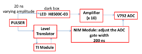 |
The H8500C-03 PMT was placed inside a dark box together with a green Light Emitting Diode (LED) to be used as a source of photons. A pulser was used to power the LED with a pulse width of 20 ns and of varying amplitude from 0.85 to 4 V. The same pulser was used to trigger the data acquisition. The signal from the PMT was passed through a low-noise 10X amplifier and then was sent to a CAEN v792 charge integrating Analog-to-Digital Converter (ADC). The software used for data acquisition was CODA 2.5, developed at Jefferson Lab. Pedestal events were taken before each run to monitor the stability of our system. For pedestal runs the LED was not powered thus only the background signal from the PMT in the absence of light along with any electronic circuit noise was recorded by the ADC. For the entire duration of the experiment the pedestal peak position and its width have been very stable, with a standard deviation of the pedestal distributions less than 6 ADC channels. For the magnetic field measurements we used additionally an iron-core “C” magnet with its power supply and a gaussmeter to monitor the magnitude of the field. More details on the experimental setup for the magnetic field tests will be given in Section 4.
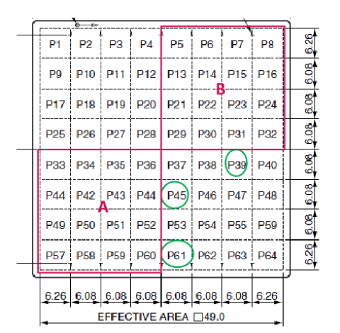 |
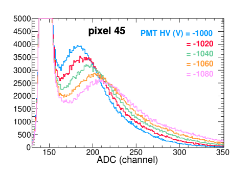
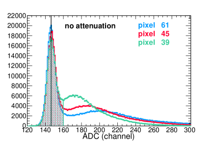
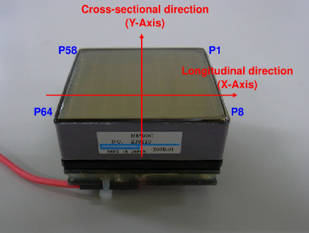
A schematic of the PMT division in pixels is shown in Fig. 2. We recorded the output from three individual pixels, 39, 45 and 61, and from 2 groups of 16 pixels, “quad A” and “quad B”, as shown. Two pixels were selected to evaluate whether an edge pixel (61) behaves differently under a magnetic field than a more central pixel (45). Pixel 39 was chosen because it had one of the lowest relative gains in the Hammamatsu gain map shipped with the device. Pixel 61 had the highest gain of all 64 pixels, while 45 and 39 were labeled with a relative output of 79% and 54%, respectively, when compared to the highest output. The signal from quad A represents the sum over 16 pixels with relative outputs ranging from 55% to 97% while quad B gets contribution from pixels with relative gains between 48% and 86%. For the SoLID application a four quad division of each PMT would be a reasonable choice as output.
3 Single-photoelectron Measurements
The methodology of single-photoelectron identification relies on the quantum nature of the process of electron extraction from the PMT photocathode where at the microscopic level an electron (also called photoelectron) is extracted from the photocathode via the photoelectric effect by one incident photon. In reality not every single absorbed photon will release a photoelectron. The probability of photoemission is quantified by the quantum efficiency defined as the ratio of output electrons to incident photons which depends on several parameters specific to the photocathode material such as the reflection coefficient, full absorption coefficient of photons, the work function and also on the energy of the incident photon. Typically, materials used as visible range photocathodes have quantum efficiencies below 30% which means that for a given number of photons incident on the photocathode only a relatively small fraction will be converted into electrons.
In our experiment a trigger was formed every time a pulse was sent to the LED. The pulse amplitude was reduced until, on average, only 0 (i.e. pedestal events) to one photoelectron was being produced at the photocathode per pulse. The yield of photons was then varied in small steps by adjusting the pulse amplitude in order to change the fraction of single photoelectron events to pedestal events in a run. The expectation was that the single photoelectron distribution will peak at the same location on the ADC histogram when compared to the pedestal position since for a fixed PMT high voltage the gain of the PMT is independent of the magnitude of incoming photons yield.
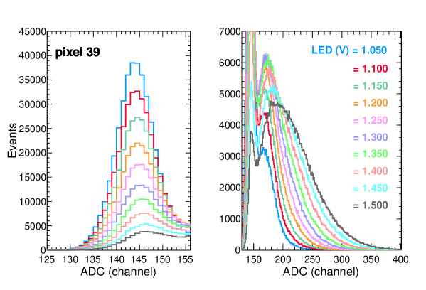
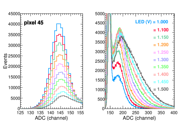
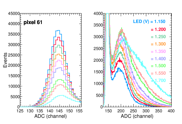
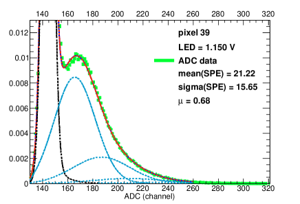
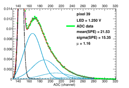
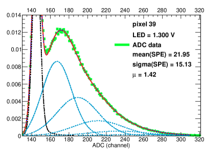
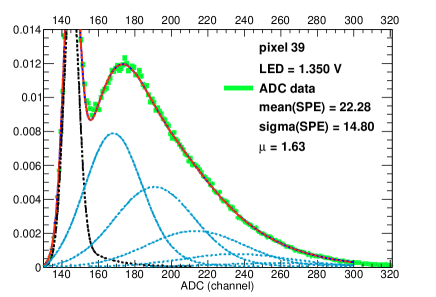
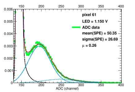
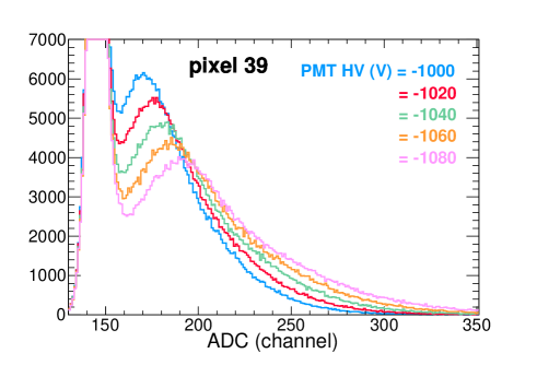
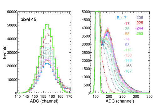
Our measurements taken on pixels 39, 45 and 61 are shown in Fig. 3. The amplitude of the pulse that powered the LED was varied between 1–1.7 V in small steps. For the lowest amplitude pulse the single photoelectron peak is visible in all pixels but the predominant contribution to the run comes from pedestal events. As the yield of photons per trigger increases, the fraction of single photoelectron events within a run becomes larger. For the highest pulse amplitude, 2 photoelectron events are produced in a non-negligible fraction as well. It can be seen qualitatively that the peak of the single photoelectron distribution is separated from the pedestal peak by approximately the same number of ADC channels per pixel. Based on Hamamatsu’s pixel gain map, pixel 39 has the lowest gain of the three pixels under measurement while 61 the highest. This is clearly visible in Fig. 3 when looking at the pedestal to single photoelectron peak separation. For the highest gain pixel, 61, the measurement taken with a LED setting of 1.7 V shows 1 and 2 photoelectron peaks as distinguishable features of the ADC distribution.
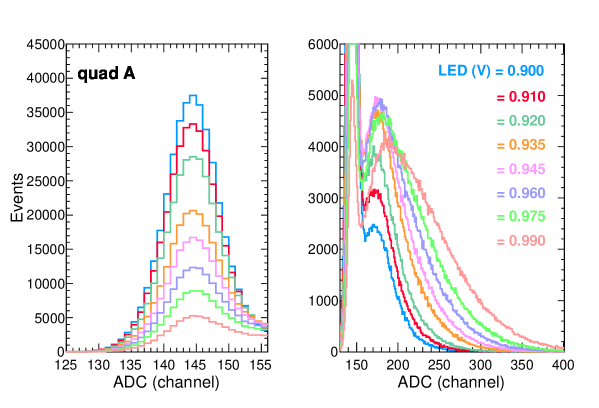
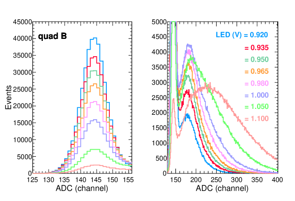
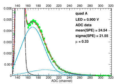
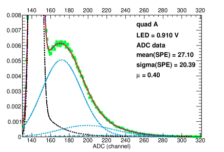
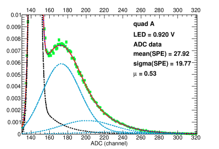
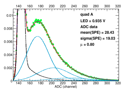
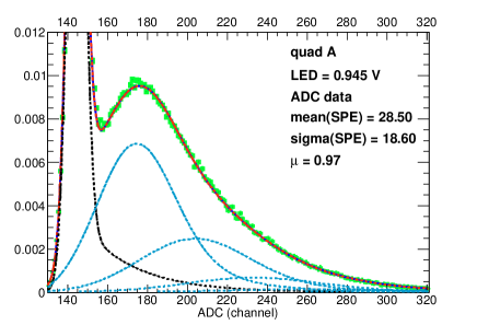
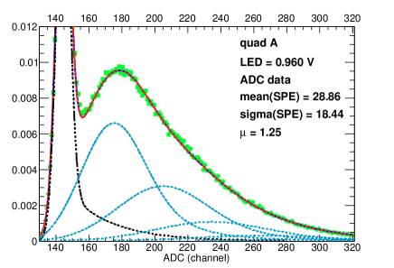
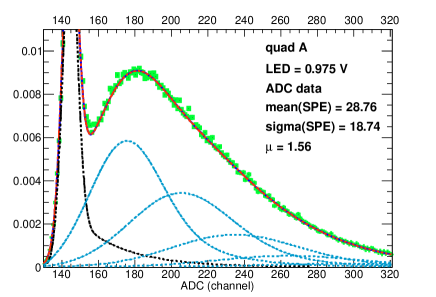
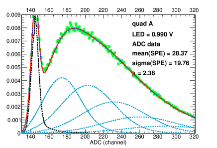
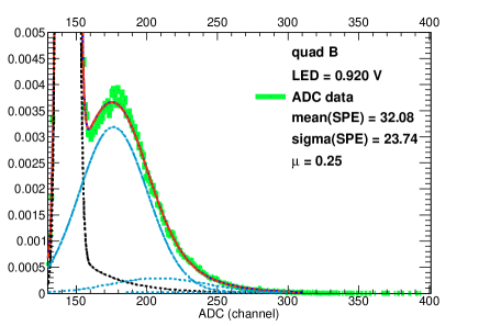
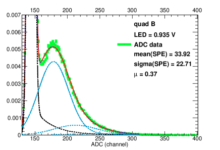
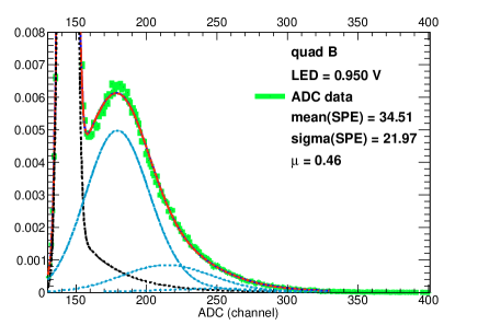
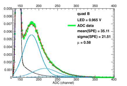
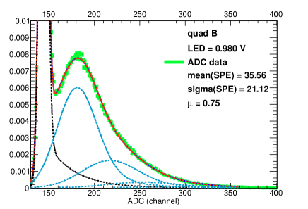
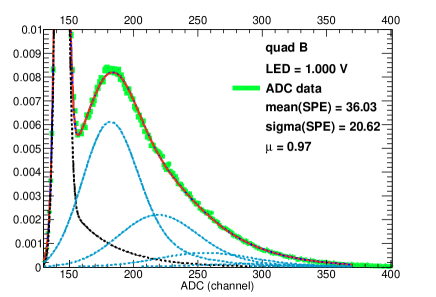
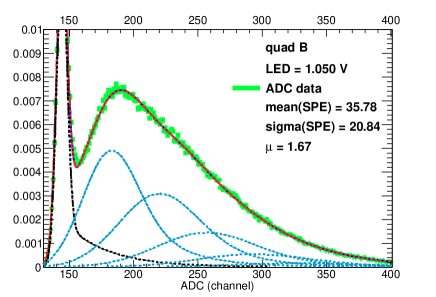
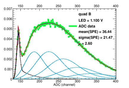
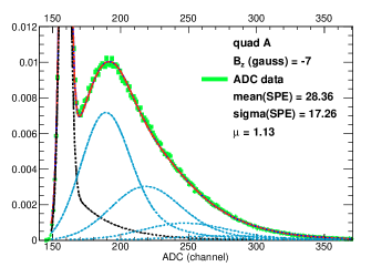
Of marked interest for SoLID’s application is the single-photoelectron response of groups of pixels. Figure 4 shows our measurements on two groups of 16 pixels labeled quad A and quad B as indicated in Fig. 2. We use the same procedure for single-photoelectron detection as for single pixels but we start with a lower LED voltage (i.e. lower yield of photons) since we need only one pixel from the group of 16 to respond per event. Given that each pixel of the group has a different gain, the charge resulting from a single photoelectron extracted from the photocathode can be different per event if different pixels respond. Thus the resulting ADC distributions shown in Fig. 4 can be viewed as a superposition of single pixel ADC distributions with possibly different gains. Nevertheless, our measurements show that the single-photoelectron signal is still clearly identifiable when summing over the output of 16 pixels.
3.1 Single-photoelectron Characterization
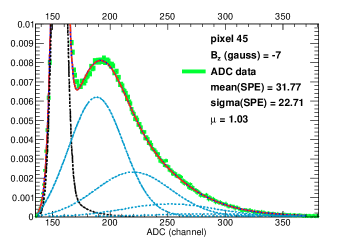
The ADC single-photoelectron spectra have been analyzed using a PMT response function developed by Bellamy and collaborators bellamy [2] which parametrizes the photoconversion process at the photocathode and the electron collection and amplification through the dynode chain. The conversion of photons into electrons at the photocathode is described by a Poisson distribution while the response of the multiplicative dynode chain is parametrized using a Gaussian distribution. The PMT response function accounts also for various background processes which would generate additional charge like thermoelectron emission from the photocathode and/or dynode chain, leakage current in the anode circuit, etc. The background is parametrized by a combination of Gaussian and exponential functions. The realistic response function is then given by:
| (1) |
where
| (2) |
with and . Here is the pedestal and is the error function. There are seven fit parameters: and define the pedestal position and width, and describe the discrete background and the remaining three parameters, , and characterize the spectrum of the real signal. Of the latter three parameters, is proportional to the intensity of the light source, and and characterize the amplification process of the dynode system.
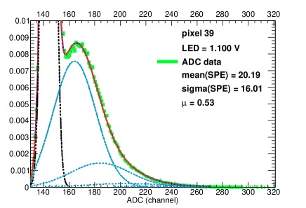
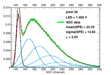
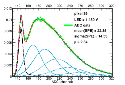
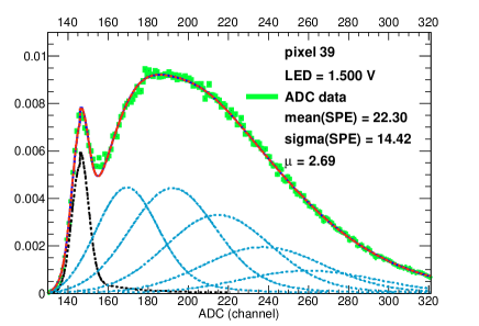
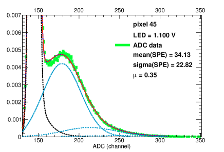
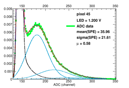
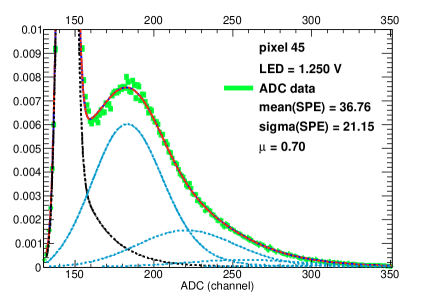
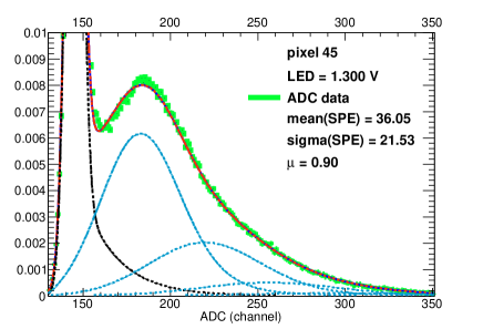
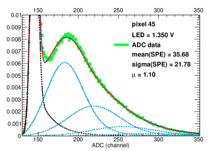
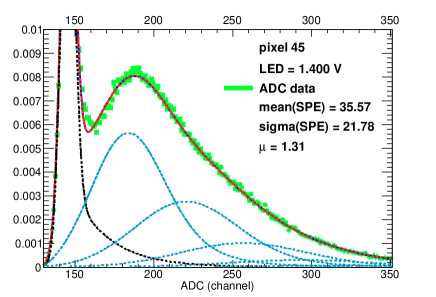
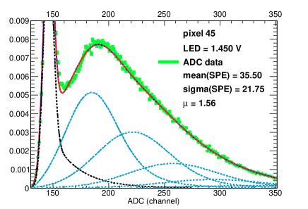
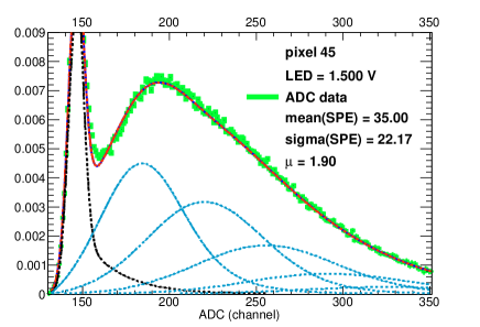
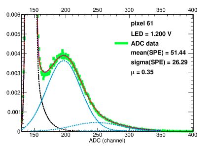
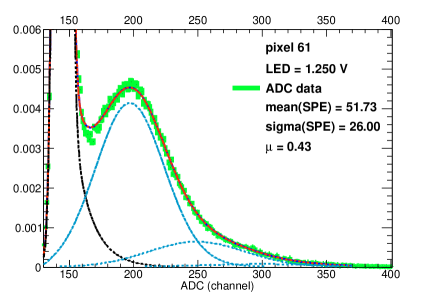
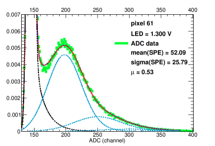
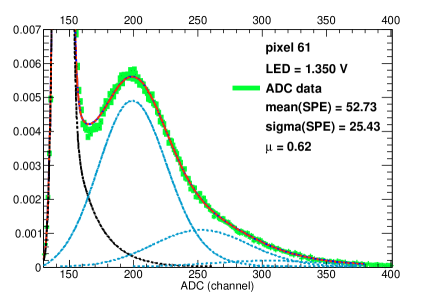
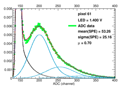
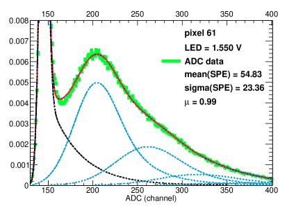
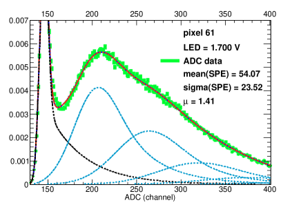
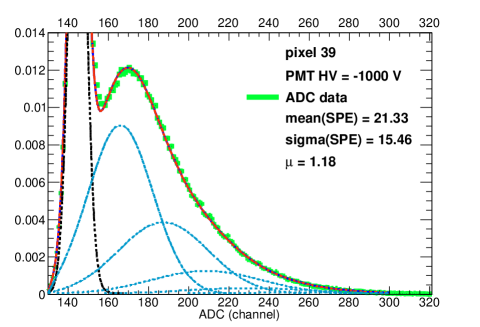
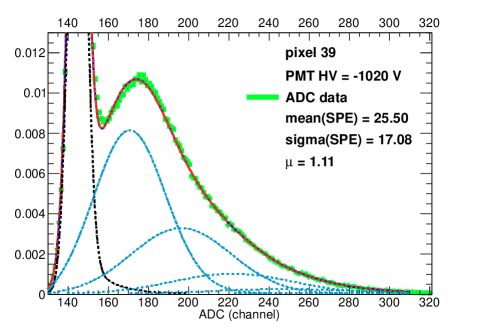
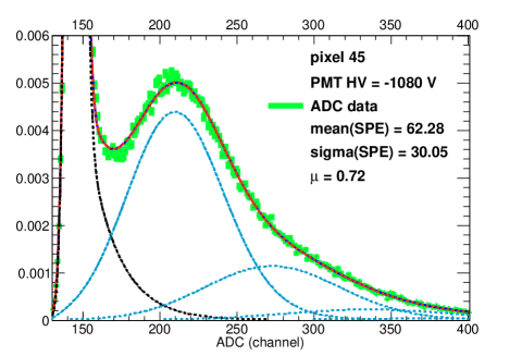
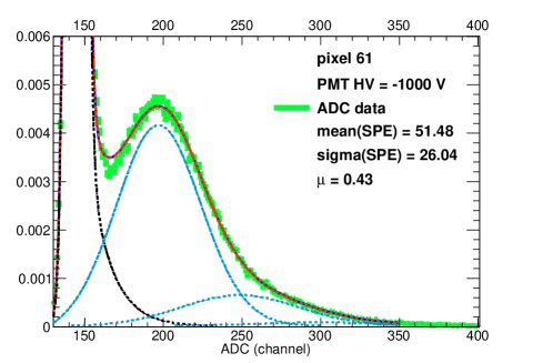
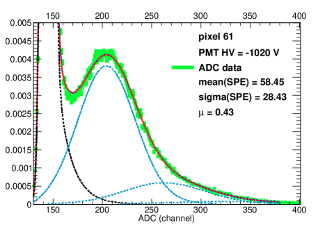
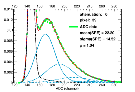
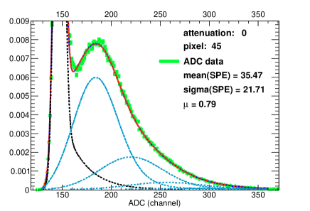
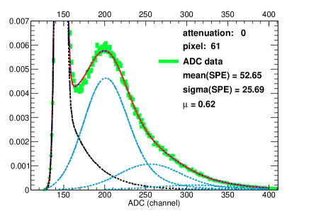
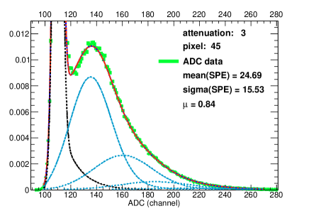
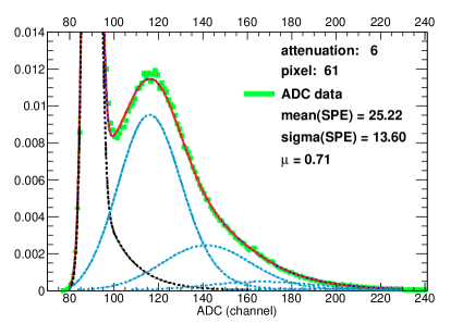
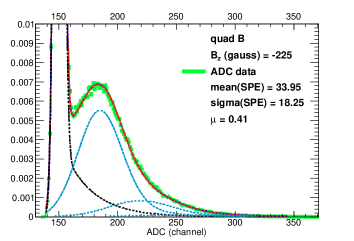
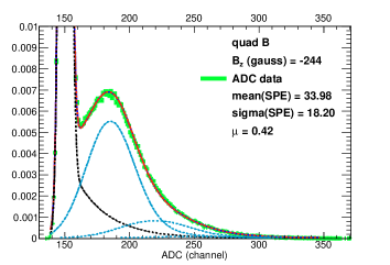
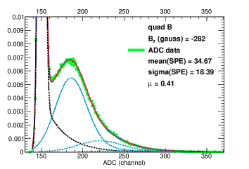
Our fits of the single photoelectron ADC spectra are shown in Figs. 5, 6, 7, 8 and 9 for pixel and quad measurements. Each of the 8 panels in Figs. 5 to 9 shows the ADC distribution for one LED setting along with the fit where various contributions have been plotted on the same graph. The solid red curve displays the full fit function as given by Eq. 1. The black dashed curve shows the background contribution only and the blue dotted curves represent the photoelectron distributions coming from the real signal.
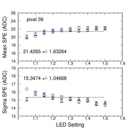
The location of the single photoelectron peak (in ADC channels above pedestal) mean(SPE) which is a measure of the gain and the standard deviation of the single photoelectron distribution as extracted from the fit, are also shown together with the Poisson mean describing the average number of photoelectrons, . For each of the pixels and quads we show fits to the ADC distributions corresponding to various LED settings. Assuming the fit function characterizes reliably the PMT response, the expectation is that for an increasing LED voltage per pixel or quad and will remain constant while the average number of photoelectrons, , will increase. This pattern is indeed observed for all the pixels and quads studied. Also the charge corresponding to a single photoelectron for each of the three individual pixels confirms the gain per pixel measurements provided by Hamamatsu where pixel 39 has the lowest gain of the pixels tested while 45 and 61 have higher gains (in this order).
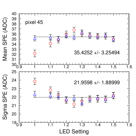
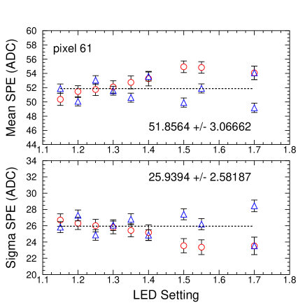
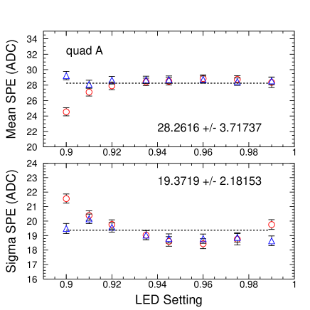
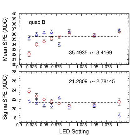
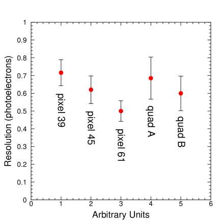
We summarize our fit results in Fig. 10 where we plot and v.s. LED pulse voltage, characterizing the single photoelectron distribution as extracted from the fit for all LED settings for the three individual pixels and for the two quads. For all outputs we performed two sets of fits. In one case, we fit allowing all parameters to change during the minimization process; these results are represented in Fig. 10 by the empty red circles. We also fit fixing the background parameters, and , and the results are shown by the blue empty triangles. To extract the average mean and standard deviation characterizing the single photoelectron distribution for pixels and quads we then perform a linear fit to and using a zero order polynomial (dashed black line in Fig. 10). We take the largest deviation of the measurements from this fit as the uncertainty of the quantity extracted. Both the average mean and standard deviation of the single photoelectron distribution together with their associated uncertainties are shown Fig. 10 for all pixels and quads tested. The uncertainty on the mean is mostly within 10% (slightly larger for quad A) and of a similar magnitude for the standard deviation.
We calculate the resolution for single photoelectron detection from the fit results as the ratio of the standard deviation and the mean. As seen in Fig. 10, bottom right panel, pixel 39 with the lowest gain has the lowest resolution of about 0.7 photoelectrons while for the highest gain pixel, 61, we obtain 0.5 photoelectrons. For quads the resolution is again below 1 photoelectron. The demonstrated performance of group of pixels is quite satisfactory for applications like SoLID where the single photoelectron identification is crucial. Overall, although the H8500C-03 has a typical gain several orders of magnitude lower than PMTs conventionally used for Cherenkov light detection, it can clearly resolve single photoelectron signals with a resolution of less than one photoelectron.
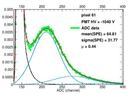
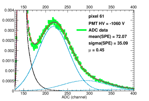
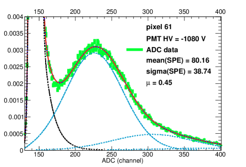
3.2 Gain Measurements
We took measurements to determine the gain of each of the three pixels tested. Once the single photoelectron signal is identified the gain was extracted using:
| (3) |
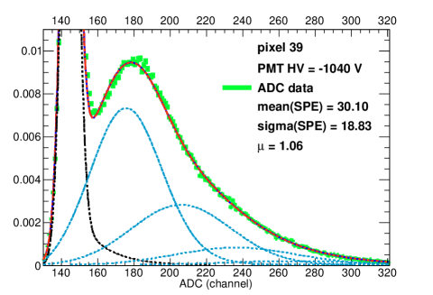
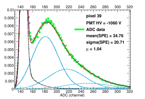
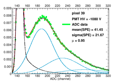
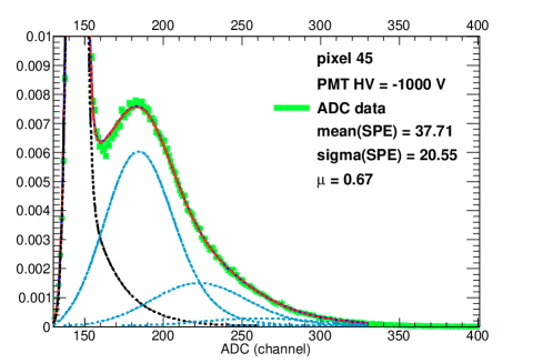
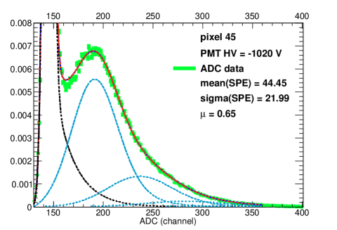
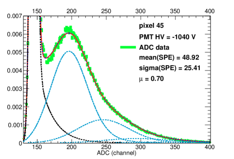
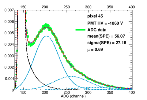
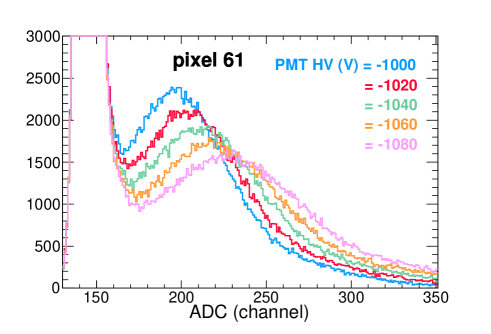
The CAEN V792 ADC we used has a resolution of 100 picoCoulomb per bin. The PMT signal was amplified by a factor of 10 and , the number of ADC channels above the pedestal corresponding to the single photoelectron peak, was extracted by fitting the ADC distributions as explained in the previous subsection. We measured the boost in the PMT gain by increasing the PMT high voltage from a nominal value of -1000 V to -1080 V in steps of 20 V (the maximum safe high voltage value is -1100 V according to Hamamatsu’s specifications). The ADC distributions for pixels 39, 45 and 61 for varying PMT high voltage settings are shown in Figs. 11, 12 and 13 together with our fits. During the high voltage scan the LED setting was kept constant for each pixel. Thus, as the PMT high voltage increases it is expected that the pixel gain will increase but the average number of photoelectrons will remain constant. Indeed, as seen in Figs. 11, 12 and 13, with each 20 V increase in the PMT high voltage the pixel gain grows by 10-15% as indicated by while the average number of photoelectrons given by remains the same.
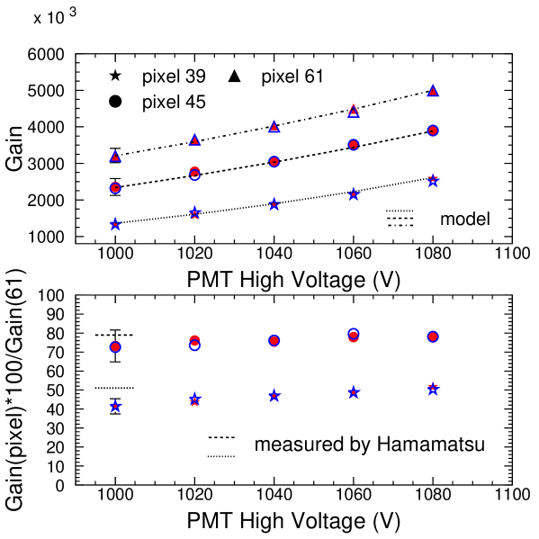
The gain extracted according to Eq. 3 for each of the three pixels tested is shown in Fig. 14, top panel, together with a model that parametrizes the change in gain with voltage of a 12 dynode stage PMT as where is a constant and is determined by the structure and material of the dynode. The curves shown in Fig. 14, top panel, represent the model prediction when using the coefficients and as extracted from measurements taken at -1000 V and -1080 V. We also calculated the relative gain for pixels 39 and 45 with respect to the highest gain pixel, 61, and our data, shown in Fig. 14, bottom panel, are in agreement with the measurements from Hamamatsu at -1000 V (dashed and dotted lines).
3.3 Output Matching
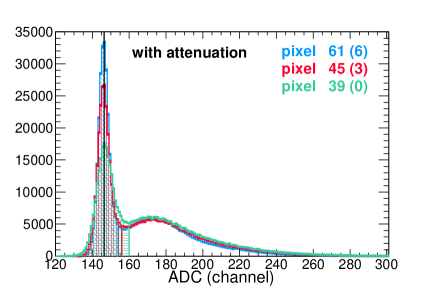
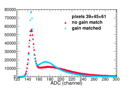
As pointed out in previous subsections, gain non-uniformities up to a factor of two or more between pixels are common and this can result in a decrease in the single photoelectron detection resolution when outputs from several pixels are summed. The effect can be corrected for by normalizing the output of pixels with higher gains to the output of the lowest gain pixel. This may be achieved by adding a simple resistor-based voltage divider into the readout circuit so that the output of the higher gain pixels is attenuated to match that of the lowest gain pixel. We followed this procedure to match the output of pixels 45 and 61 to that of pixel 39 and we show our results in Fig. 15. The first two panels on the left and the first panel on the right display the single photoelectron ADC distributions for pixels 39, 45 and 61 together with a fit which shows the three pixels to have varying gains, up to 60%, as indicated by the fit parameter . To emphasize the effect we superimposed the ADC distributions of the three pixels on the second right panel. We passed the outputs from pixels 45 and 61 through a rotary attenuator and the attenuated signals as recorded by the ADC are shown in the third left and right panels, respectively. We used 3 and 6 db attenuation for pixel 45 and 61 to match the output of pixel 39. After attenuation, the output of the three pixels is very similar, within 10%, as indicated by the fit parameter . The bottom left panel shows the superposition of the ADC distributions from the three pixels after attenuation and it can be seen that the single photoelectron peak is positioned at the same location with respect to the pedestal. Lastly, in the bottom right panel we show the sum of the ADC spectra of all three pixels before (red triangles) and after (blue starts) output matching. The improvement in the resolution for single photoelectron detection is evident.
4 Magnetic Field Measurements
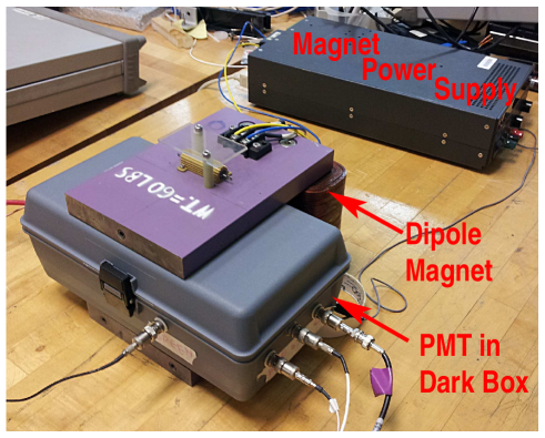
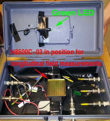
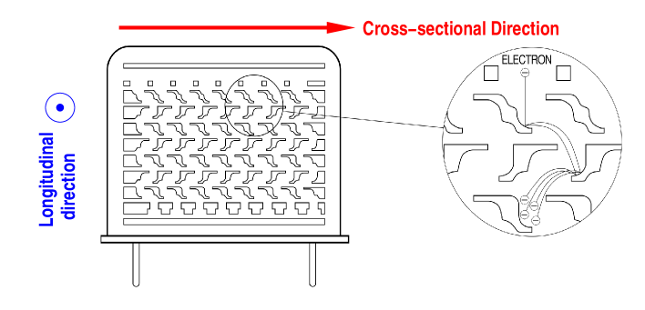
In Figs. 16 and 17 we present few pictures of the experimental setup used to study the PMT behavior in magnetic field. In Fig. 16, top left panel, we show the PMT dark box (in grey) in between the dipole magnet plates (purple) with the coils visible at the back of the dark box. The magnet cable leads (in blue and yellow) connect the coils to the power supply. The four signal cables corresponding to outputs from pixel 45, 61, quad A and quad B can also be seen. In the panel on the top right, we show the PMT positioned inside the dark box for longitudinal magnetic field measurements, i.e. the dipole magnetic field is perpendicular to the face of the PMT. In what follows, we will refer to this field orientation as . The LED is attached to the box so that it can illuminate the face of the PMT. In the bottom panel the transverse field orientations are shown (i.e. field perpendicular to the sides of the PMT) with respect to the PMT and we labeled those as and . The metal channel dynode structure of the PMT and the transverse field orientations are also depicted in Fig. 17. Note that the PMT response to magnetic field is symmetric with respect to a rotation around the longitudinal field axis. For a given alignment axis we can switch the field direction (plus or minus) by swapping the leads that power the coil. To expose the PMT to either purely longitudinal or transverse field components we monitored closely the PMT positioning relative to the magnetic field orientation and built rigid supports to hold the PMT in place and avoid possible position shifts during measurements.
We performed two sets of measurements to study the PMT signal loss in magnetic fields. In one case we tuned the yield of (LED) photons to trigger large PMT signals, at the level of 30 to 50 photoelectrons, and in the zero field configuration this became one baseline. We then increased the magnetic field, in steps of 20 Gauss and followed the deviation of the PMT response from the baseline. For the second set of measurements the same procedure was followed but photon yields were tuned to provide small PMT signals, at the single photoelectron level.
4.1 Effects of Magnetic Field on Large Signals
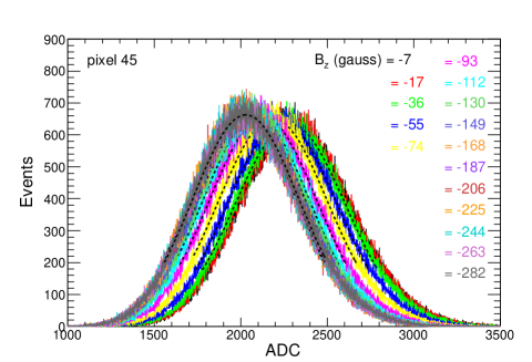
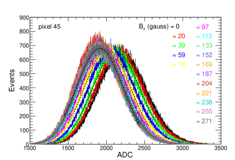
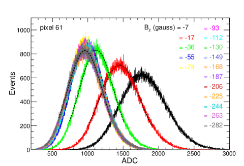
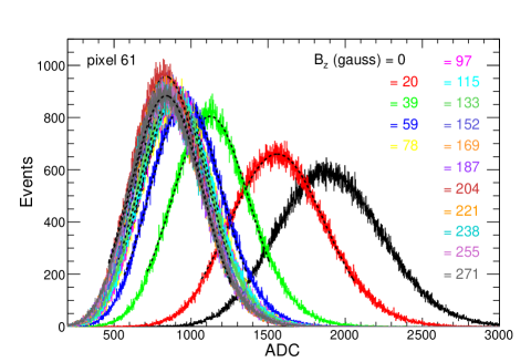
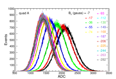
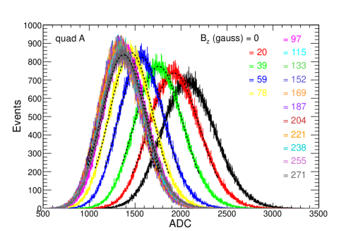
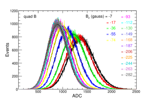
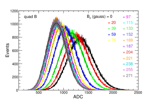
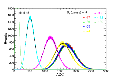
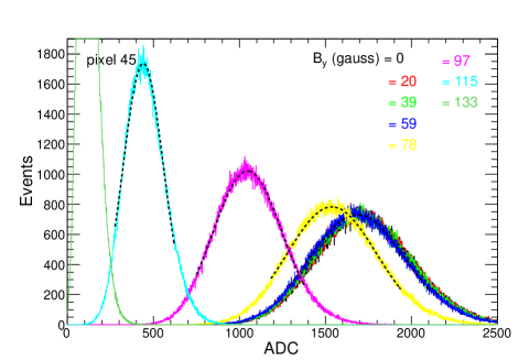
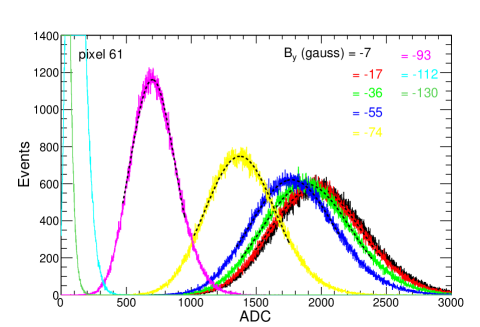
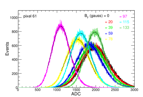
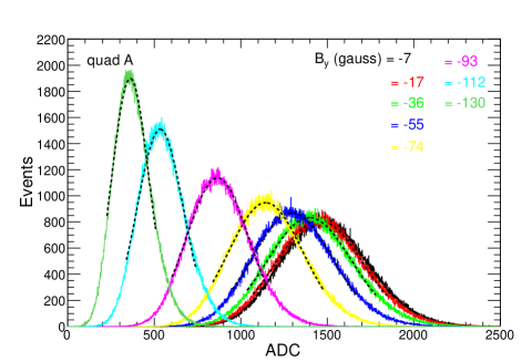
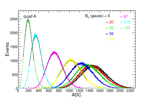
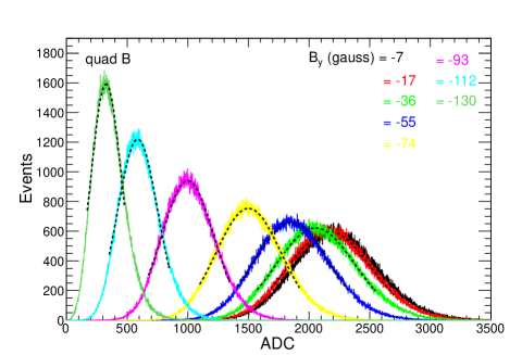
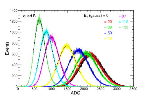
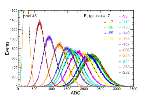
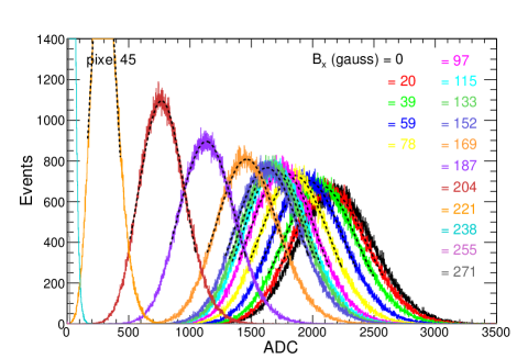
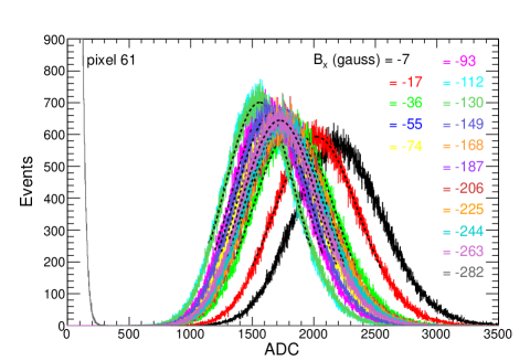
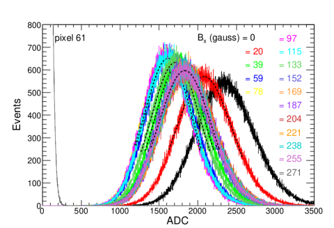
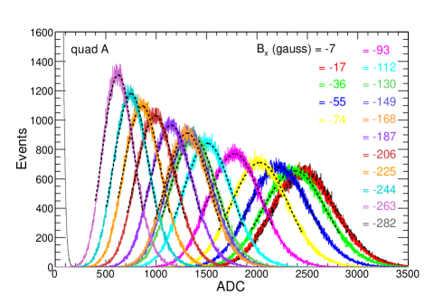
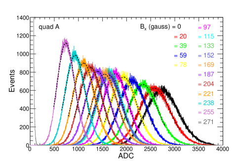
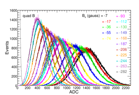
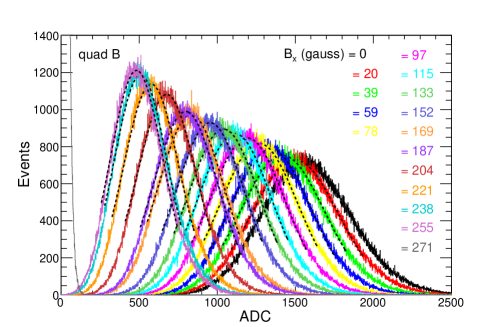
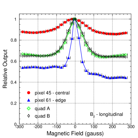
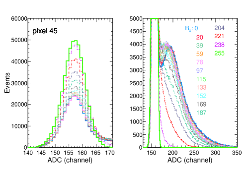
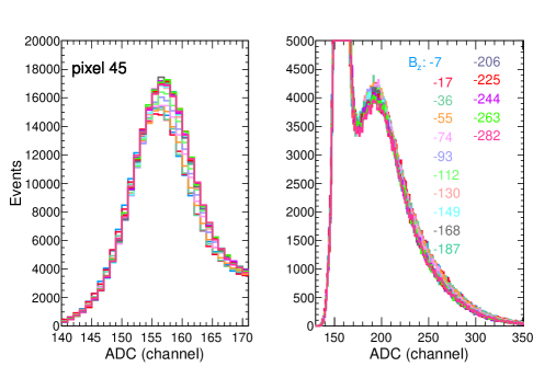
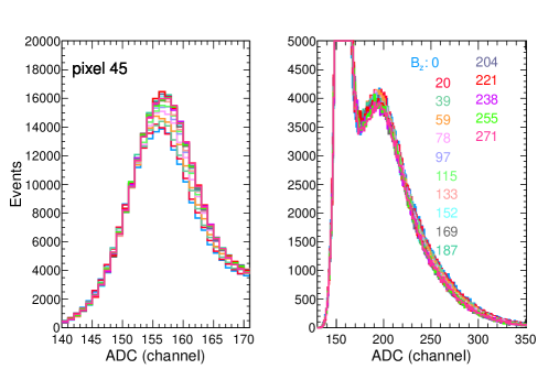
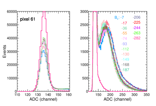
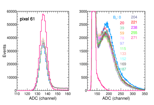
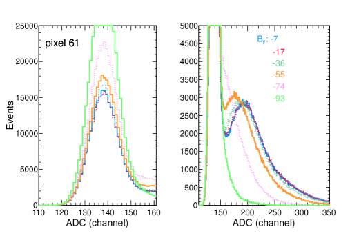
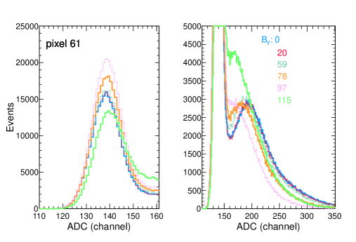
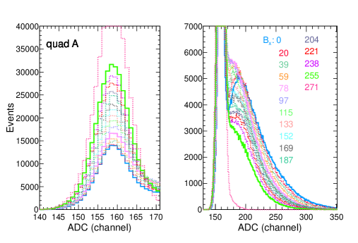
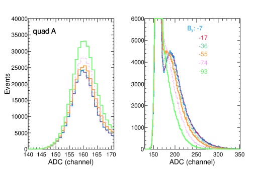
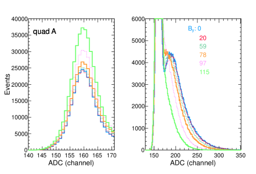
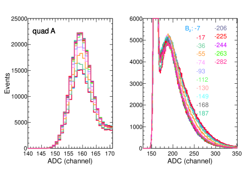
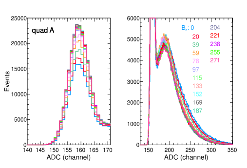
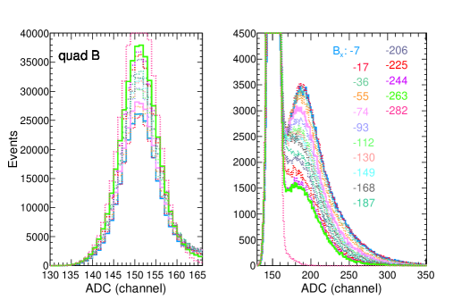
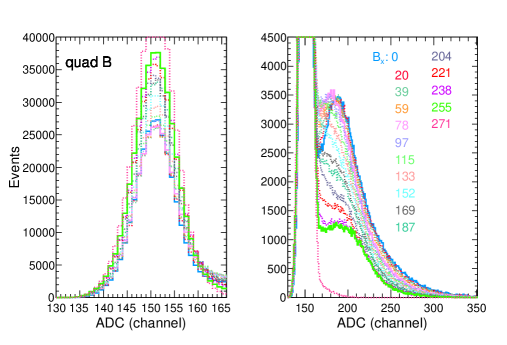
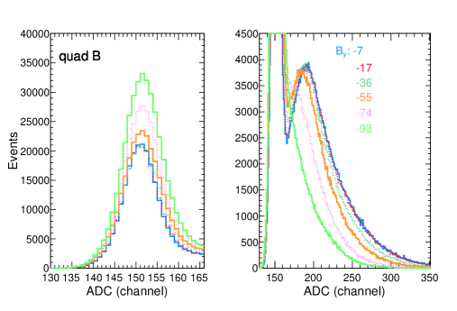
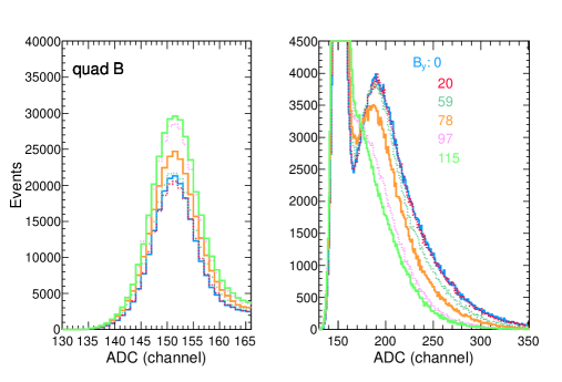
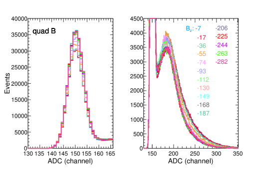
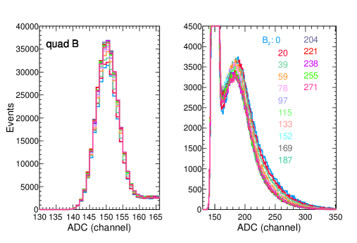
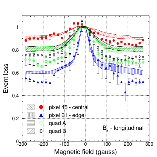
In Figs. 18, 19 and 20 we present the change in the output with magnetic field as recorded by the ADC from pixels 45 and 61 and from the two groups of 16 pixels, quad A and quad B. Each of the ADC distributions shown were recorded at a given field setting and have been pedestal subtracted. While there is a small signal degradation for the central pixel (45) with an increasing longitudinal field, as seen in Fig. 18, top left and right panels, the edge pixel (61) experiences greater losses as indicated by the more pronounced shift of the mean of the ADC distributions when going from the no field configuration (black curve) to a magnetic field close to 300 Gauss (gray curve) (second left and right panels). The quads’ response to an increasing field can be viewed as an average over the central and edge pixels behavior. It is interesting to note that the signal progressively degrades with an increasing longitudinal magnetic field up to about 100 Gauss but then the degradation saturates and the output stays constant up to field magnitudes of 300 Gauss. This pattern is observed for both central and edge pixels as well as for quads.
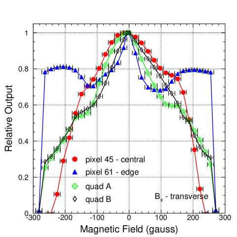
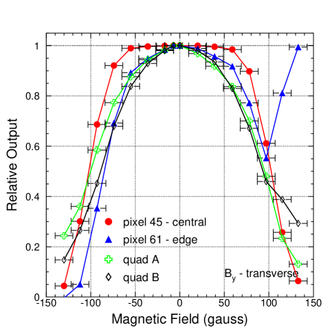
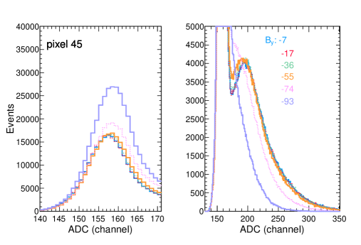
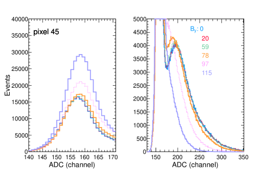
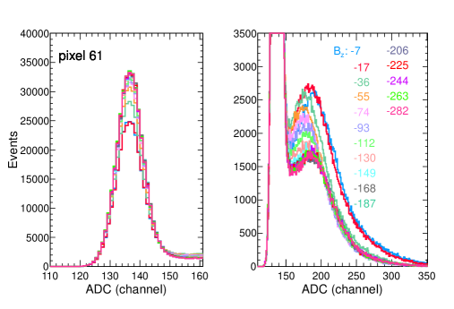
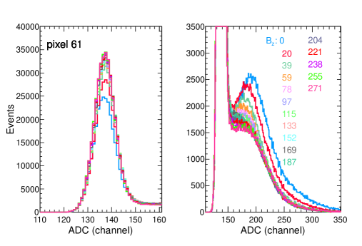
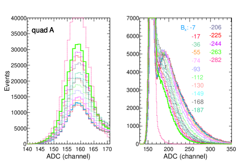
The loss of signal in a transverse magnetic field and is more dramatic as seen in Figs. 20 and 19. In particular, the PMT output degrades rapidly under a transverse field, being reduced to zero at 130 Gauss. A transverse field has a similar effect at 244 Gauss for the central pixel and at 282 Gauss for the edge pixel and quads. The variation of the edge pixel output with a transverse magnetic field follows a different pattern as seen in Figs. 20 and 19, second left and right panels.
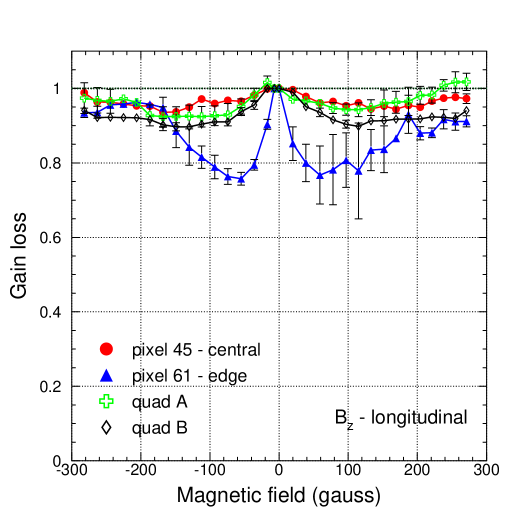
In Fig. 21 we summarize our studies of a longitudinal and transverse magnetic field effect on large outputs from central and edge pixels and groups of pixels. To quantify the effects we fitted each of the pedestal subtracted ADC distributions with a Gaussian function as shown in Figs. 18, 19 and 20. For each magnetic field setting the mean of the ADC distribution thus obtained has then been normalized to the no-field value. The results for a longitudinal magnetic field are shown in Fig. 21, first panel. The same pattern emerges when looking at the variation of the output with field from central and edge pixels and from quads. There is only a difference in the magnitude of the field induced losses, the edge pixel experiencing the largest reduction, at most 55%, and the central pixel the smallest, at most 15%. If the quad configuration were to be used in production, then a 10% signal loss would be expected at 30 Gauss. For applications like SoLID where the PMT is placed in a high magnetic field environment, up to 200 Gauss, shielding that would reduce the longitudinal field from hundreds of Gauss to 30 Gauss should be sufficient to ensure a proper functionality of the system. In practice, the longitudinal component of the field is typically the most difficult to shield, so a PMT like H8500C-03 which experiences only small output losses up to longitudinal fields of the order of tens of Gauss makes more practical and cost-effective shielding designs possible. The bottom panels summarize the signal reduction in transverse magnetic field and , respectively. Here the losses can be very large even at modest field values and very good shielding against transverse fields would be necessary for a good functionality of the PMT.
4.2 Effects of Magnetic Field on Single Photoelectron Signals
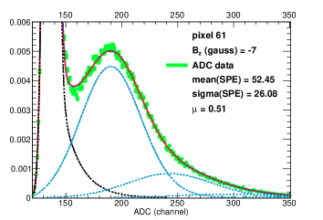
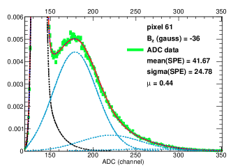
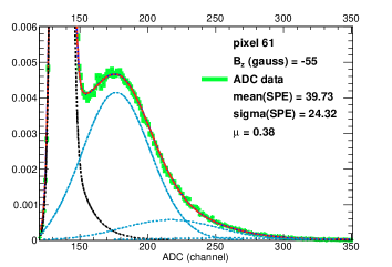
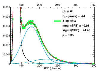
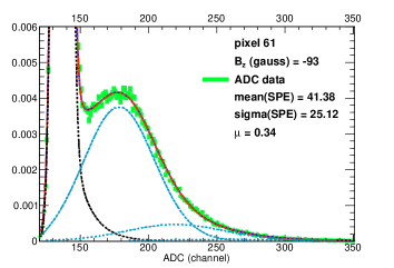
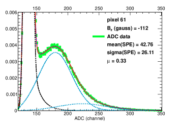
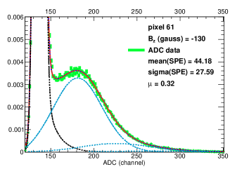
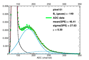
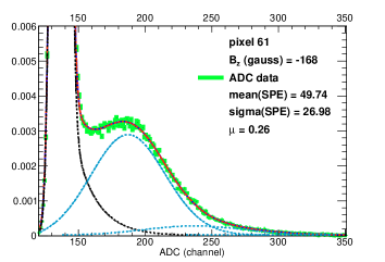
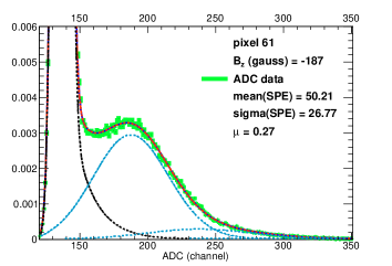
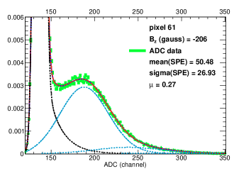
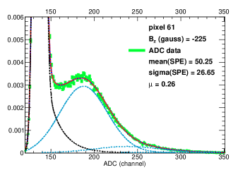
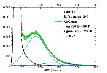
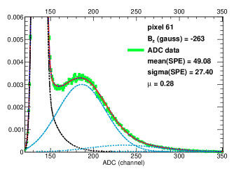
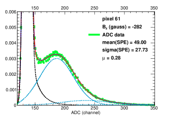
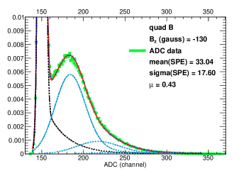
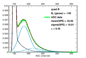
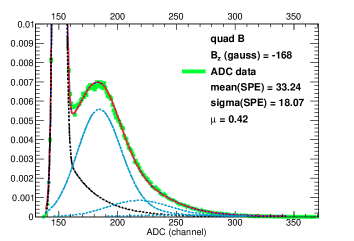
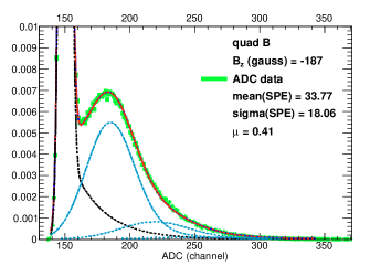
We studied the effect of a longitudinal and transverse magnetic field on signals at the single photoelectron level as well. ADC distributions from pixel 45, 61 and quads A and B are shown in Figs. 22, 23, 24 and 25 for various field settings. We highlight the pedestal and signal regions separately for all settings. After tunning the LED to maximize the output of single photoelectrons, we applied a magnetic field and varied its magnitude in small steps. The purpose of the study was to provide insight into the mechanism by which the pixel and quad outputs get diminished with increasing magnetic field. In particular there could be two dominant mechanisms by which the signal is lost. One hypothesis is that the applied magnetic field would disrupt the electrical field that focuses the photoelectron extracted from the photocathode onto the first dynode. In our case this type of event would “transfer” hits from the signal region to the pedestal region and the position of the single photoelectron peak would not be affected in the ADC distribution. Another possible effect could be the loss of gain down the dynode chain as the magnetic field applied disrupts the amplification. This would result in a diminishing gain with field and would be visible as a smaller separation between the single photoelectron peak and the pedestal on the ADC distribution. The latter effect can be compensated for by increasing the high-voltage or otherwise amplifying the signal. The former scenario, however, cannot be corrected as the initial single photoelectron is lost.
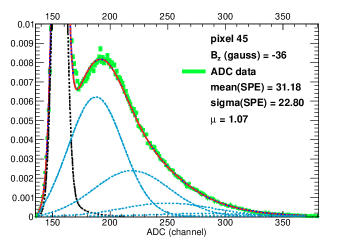
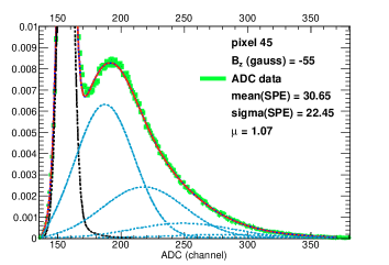
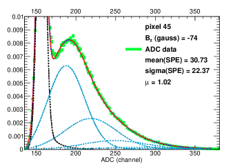
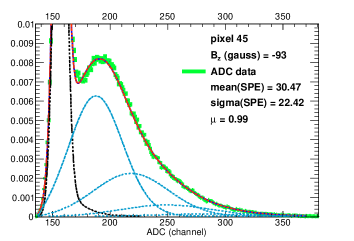
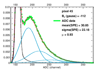
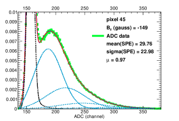
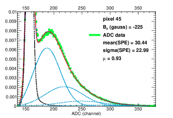
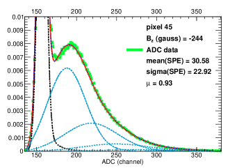
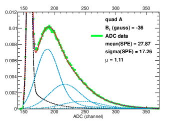
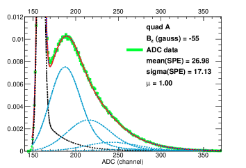
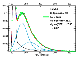
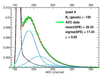
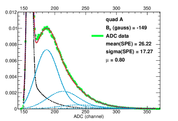
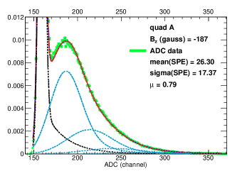
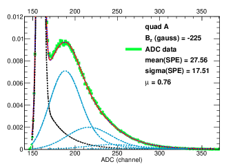
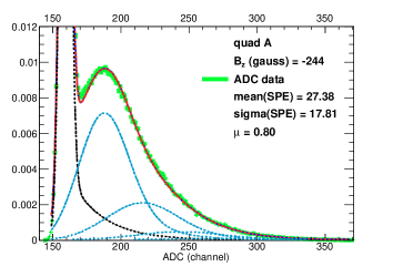
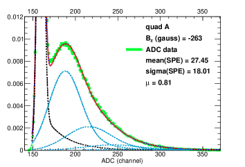
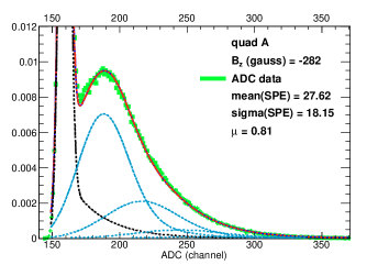
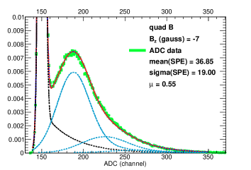
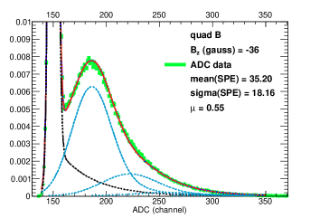
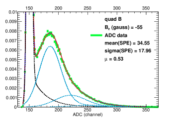
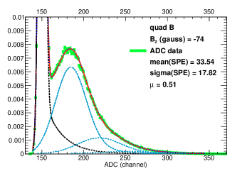
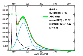
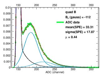
Given the practical complications associated with shielding, of particular interest is understanding the effect of a longitudinal magnetic field on single photoelectron outputs. We used the PMT response function and fitting procedure described in Section 3 to fit the ADC distributions from pixels 45 and 61 and from quads A and B for various longitudinal field settings (Figs. 22, 23, 24, 25, bottom panels). Our fits are shown in Figs. 26, 27, 28 and 29. It can be seen that the fit was stable up to the highest magnetic field setting for pixels and quads allowing a reliable extraction of the fit parameters associated with the gain, , and the average number of photoelectrons, . The fit results are summarized in Fig. 30 where we plot, on the left panel, and, on the right panel, .
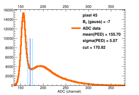
In addition, we used an integration procedure to quantify the loss of single photoelectrons due to magnetic field. In Fig. 31 we show the ADC distribution from pixel 45 for a magnetic field setting of Gauss. The pedestal distribution has been fit (the mean and standard deviation associated with the pedestal are given in Fig. 31) and we used the standard deviation thus extracted to place a cut 3 standard deviations away from the mean to formally separate the signal from pedestal (full blue line in Fig. 31). Then the ratio of signal to total events has been calculated for each field setting as the ratio of the ADC distribution integral with the three sigma cut as the lower limit and the integral over the full range ADC distribution. We also varied the cut by one sigma around the central cut (dashed blue lines in Fig. 31) and we recalculate the ratios. The results for all longitudinal field settings normalized to the no field setting are shown as bands for pixels and quads in Fig. 30, right panel. The results obtained when using the three sigma cut are plotted as central value with the width of the bands given by the one sigma cuts around the central cut. The results obtained utilizing the two methods agree within 10%.
For pixel 45 there is at most a 5% loss of gain as indicated by the red circles in Fig. 30 (left panel) and up to 15% losses associated with the photoelectron extracted from the photocathode missing the first dynode (right panel). This is also evident in Fig. 22, bottom panels, where the progression of the ADC distribution with a longitudinal () magnetic field shows that the position of the single photoelectron peak with respect to the pedestal remains mostly unchanged during the field scan while the fraction of signal to pedestal events decreases as the field increases. A very similar pattern is observed for pixel 61: there is at most 15% decrease in overall gain as seen in Fig. 30 (right panel, blue triangles) but the dominant effect is the misfocusing of the photoelectron extracted from the photocathode which can lead to losses up to 50%. This effect is clearly visible in Fig. 23, bottom panel. The same conclusions apply to the quads behavior in a longitudinal magnetic field: there is little gain loss, no more than 5% (Fig. 30, left panel, green crosses and black diamonds) but up to 30% single photoelectron losses (Fig. 30, right panel).
In a transverse field pixel 45 and the two quads experience a drastic loss of single photoelectrons as shown in Figs. 22, 24 and 25, top panels. The same qualitative trend is seen here as in Fig. 21, left bottom panel, where the change of large outputs with a transverse field was displayed. In both configurations the output from the central pixel is reduced to noise at 240 Gauss and quads experience the same reduction at about 270–280 Gauss. The edge pixel (61) behaves quite differently as shown in Fig. 23, top panel: there is a relatively small loss of signal up to a field of 260 Gauss to which both mechanisms described above appear to contribute and then there is a sudden drop to zero of the output at about 280 Gauss. This is again consistent with the results shown in Fig. 21, left bottom panel.
The losses in a transverse field are dramatic for all observables. Below 50 Gauss there are no losses for the central pixel as seen in Fig. 22, middle panels, but as the field value increases the output is lost by 100 Gauss. This is consistent with the study on large signals displayed in Fig. 21, bottom right panel. The same trend is observed for the edge pixel and quads but with a faster drop of signal with field for values below 50 Gauss. At fields above 100 Gauss the edge pixel experiences a recovery of signal (see also Fig. 21, bottom right panel).
5 Conclusions
We tested one unit of the photomultiplier tube H8500C-03 with the goal of extracting its resolution for single photoelectron detection, and to study its behavior in magnetic fields of up to 300 Gauss. We measured the output from several individual pixels (chosen based on their gain and positioning in the multianode matrix), and also the summed output from 2 groups of 16 pixels. We found that the resolution for single photoelectron detection is better than one photoelectron for both individual pixels and for sum of pixels in spite of the relatively low gain of the PMT and pixel-to-pixel gain non-uniformities. This PMT is, therefore, suitable for applications where the single photoelectron detection is necessary. Our magnetic field tests revealed that a large longitudinal field, up to 300 Gauss, induces a relative signal reduction of at most 55% for an edge pixel and of at most 15% for a central pixel. The signal degradation in transverse magnetic fields is significantly more pronounced, however, such transverse fields are also the easiest to shield in practice. Our studies of single photoelectron output reduction with magnetic field point to the field induced loss of the photoelectron extracted from the photocathode as primary cause of signal loss. With appropriate shielding this PMT could function well in high magnetic field environments.
Acknowledgment
The collaboration wishes to acknowledge the Detector Group at Jefferson Lab: Drew Weisenberger, Jack Mckisson, and Carl Zorn for their help with the PMT readout. We would also like to thank the Hamamatsu representative Ardavan Ghassemi for useful discussions. This work was supported by the U.S. Department of Energy. Jefferson Science Associates operates the Thomas Jefferson National Accelerator Facility under DOE contract No. DE-AC05-06OR23177. This work was also supported by the U.S. Department of Energy under Contract No. DE-FG02-03ER41231.
References
- [1] H. Gao, et al., Transverse spin structure of the nucleon through target single spin asymmetry in semi-inclusive deep-inelastic (e,e’) reaction at jefferson lab, Eur. Phys. J. Plus 126 (2). doi:10.1140/epjp/2011-11002-4.
- [2] E. H. Bellamy, et al., Absolute calibration and monitoring of a spectrometric channel using a photomultiplier, Nucl. Instr. and Meth. in Phys. Res. A 339 (1994) 468–476. doi:10.1016/0168-9002(94)90183-X.
|
|
 |
|
 |
 |
 |
 |
 |
 |
 |
 |
 |
 |
 |
 |
 |
 |
 |
 |
 |
 |
 |
 |
 |
 |
 |
 |
 |
 |
 |
 |
 |
 |
 |
 |
 |
 |
 |
 |
 |
 |
 |
 |
 |
|
|
|
|
|
|
 |
|
 |
|
 |
|
 |
|
 |
|
 |
|
 |
|
 |
|
 |
|
 |
 |
 |
 |
 |
 |
 |
 |
 |
|
|
|
 |
|
|
|
|
|
|
|
|
|
|
|
|
|
|
|
|
|
|
|
|
|
|
|
|
|
|
|
|
 |
|
 |
|
 |
|
 |
|
 |
|
 |
|
 |
|
 |
|
 |
|
 |
|
 |
|
 |
|
 |
|
|
 |
|
|
 |
|

|
 |

|
|
 |

|

|
 |
|
|
 |
|
|
 |
|
|
 |
|
|
 |
|
|
 |
|
|
 |
|

|
 |
|

|
 |

|
|
 |
|
|
 |
|
|
 |
|
|
 |
|
|
 |

|
|
 |

|
|
 |
|
 |