Electrically Detected Double Electron-Electron Resonance:
Exchange Interaction of P Donors and P Defects at the Si/SiO Interface
Abstract
We study the coupling of P dangling bond defects at the Si/SiO2 interface and 31P donors in an epitaxial layer directly underneath using electrically detected double electron-electron resonance (EDDEER). An exponential decay of the EDDEER signal is observed, which is attributed to a broad distribution of exchange coupling strengths from kHz to MHz. Comparison of the experimental data with a numerical simulation of the exchange coupling shows that this range of coupling strengths corresponds to 31P-P distances ranging from 14 nm to 20 nm.
I Introduction
Design and modeling of semiconductor devices requires the detailed understanding of those defects which influence the electronic properties of these devices. Electron paramagnetic resonance (EPR) is particularly suited to investigate the microscopic structure of paramagnetic defects in semiconductors Spaeth and Overhof (2003). In samples and devices, where the number of defects is not sufficient for EPR detection, electrically detected magnetic resonance (EDMR) has been established as a versatile alternative due to its orders of magnitude higher sensitivity compared with conventional EPR Lepine (1972); Brandt et al. (2004); McCamey et al. (2006); Baker et al. (2012); Schnegg et al. (2012). Most EDMR processes involve the formation of spin pairs whose spin symmetry determines the transport properties, resulting in a resonant current change when spins are flipped by microwave irradiation Schmidt and Solomon (1966); Kaplan et al. (1978); Kishimoto et al. (1981). In particular, spin-dependent recombination processes in silicon have been interpreted successfully in terms of spin pair or donor-acceptor recombination models Stich et al. (1995). An example of such a process is observed in phosphorus-doped silicon near the Si/SiO2 interface where a spin-dependent recombination process occurs via spin pairs formed by 31P donors and P dangling bond defects Hoehne et al. (2010). This spin pair not only serves as a prototype example for other spin-dependent recombination processes, but is also of interest in donor-based quantum information processing Kane (1998); Morello et al. (2010) with respect to readout of qubit states Boehme and Lips (2002), providing a spin-to-charge transfer, and decoherence introduced by interface defects de Sousa (2007). The advent of pulsed electrically detected magnetic resonance (pEDMR) techniques allows to address spin dynamics such as the formation and recombination of spin pairs, spin coherence, coherent control and readout of spins as well as spin-spin coupling Stegner et al. (2006); Huebl et al. (2008); Dreher et al. (2012).
Spin pairs are characterized by a noticeable coupling between the two spins due to their spatial proximity Lu et al. (2011). However, the coupling strength and its dependence on the spin-spin distance of such spin pairs has not been studied in detail so far. Here, we apply electrically detected double electron-electron resonance (EDDEER) to measure the coupling between 31P donors and P Si/SiO2 interface defects. We compare the experimental results with a numerical calculation of the exchange coupling and find that the observed EDDEER signal can be attributed to a distribution of spin pairs relevant for the spin-to-charge detection scheme used here with distances between about 14 nm and 20 nm.
II Experimental methods and details
Before we present our experimental results, we shortly review the basic idea of the DEER method, which is widely used in pulsed EPR e.g. to study the structure of complex molecules Milov et al. (1981); Jeschke (2002). The coupling between two spins A and B is measured by the EDDEER pulse sequence sketched in Figure 1 (b). It consists of a ---- spin echo sequence Jeschke and Schweiger (2001), including a final projection pulse Huebl et al. (2008), resonant with the A spins, where and denote microwave pulses with corresponding flipping angles and and periods of free evolution. At time after the first pulse an additional pulse is applied to invert the B spins. Taking only into account the electron spin Zeeman interaction and the exchange coupling, the spin Hamiltonian of the spin pair is given by
| (1) |
where denote the Larmor frequencies of spins A and B, denotes the exchange coupling constant and the Pauli spin operator. We neglect non-secular terms of the exchange coupling Hamiltonian since in this work Jeschke and Schweiger (2001) as well as the dipolar coupling since it is shown below that for the spin pairs in our sample. The last term in the Hamiltonian has the form of an additional effective magnetic field with its polarity depending on the mutual orientation of spins A and B. Flipping spin B after a time therefore changes the local field seen by spin A, resulting in an additional phase acquired by spin A during the spin echo pulse sequence. This results in an oscillation of the spin echo amplitude as a function of with a frequency determined by the exchange coupling . For a spin ensemble with a broad distribution of coupling constants the different oscillation frequencies will lead to a strong dephasing, eventually resulting in a decay without oscillations Klauder and Anderson (1962).
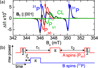
In this work we use a 20 nm-thick Si:P epilayer with a nominal P concentration of cm-3 covered with a natural oxide and grown on a nominally undoped Si buffer on a silicon-on-insulator substrate. The dimensions of the sample and Ti/Au contacts for electrical measurements are the same as in Reference Lu et al. (2011). In this type of sample, EDMR signals originate predominantly from the 31P-P recombination process Hoehne et al. (2010). The sample was mounted with the silicon [001] axis parallel to the static magnetic field , cooled to a temperature of 5 K, biased with 300 mV and illuminated continuously via a glass fiber with the white light from a tungsten lamp at an intensity 30 mW/cm2, resulting in a photocurrent of 116 A. We applied microwave pulses at -band frequencies and adjusted the microwave power such that the pulse length was 30 ns for both the 31P and P electron spins, corresponding to a microwave magnetic field of 0.6 mT. The orientation of the sample was chosen such that the P dangling bond resonance lines are degenerate, thereby facilitating the application of microwave pulses to the P. The current transients after the pulse sequence are filtered, amplified and box-car integrated from 3 s to 40 s, yielding a charge proportional to the amount of antiparallel spins at the end of the pulse sequence Boehme and Lips (2003). A lock-in detection scheme with a modulation frequency of 500 Hz, corresponding to a shot-repetition time of 2 ms, is used by applying a two-step phase cycle to the last /2 pulse of the spin echo Hoehne et al. (2012) in order to remove the background resulting from non-resonant photocurrent transients and to decrease the noise level in our measurements.
For the EDDEER measurements, the spin echo resonantly excites the P spins [spins A, Stesmans and Afanas’ev (1998), indicated by the red arrow in the continuous wave (cw)EDMR spectrum shown in Figure 1 (a)] while the inversion pulse resonantly excites both hyperfine lines of the 31P spins [spins B, , hyperfine splitting MHz Feher (1959), blue arrows in Figure 1 (a)]. We chose to invert the 31P spins rather than the P spins, since the smaller inhomogeneous broadening of the 31P transitions ( MHz) when compared to the P transition ( MHz) allows to invert a larger fraction of the 31P ensemble, resulting in a larger DEER signal Lu et al. (2011).
III Results
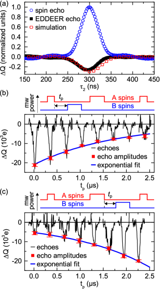
Figure 2 (a) shows an EDDEER echo (black full squares) as a function of for ns and ns together with a spin echo without the inversion pulse on the 31P spins (blue circles). The EDDEER echo is inverted when compared to the simple spin echo as expected since the additional pulse changes the spin symmetry of the 31P-P spin pair which governs the spin-dependent recombination process. The amplitude of the EDDEER echo signal is reduced by a factor of about four when compared to the spin echo. This is a result of the spectral overlap of the low-field 31P and the P line as shown in Figure 1 (a), which does not allow a fully selective excitation of the 31P spins. As a consequence, some P spins also are flipped by the inversion pulse on the 31P spins leading to a reduction of the echo amplitude. This is confirmed quantitatively by a numerical simulation of the EDDEER and spin echo pulse sequences taking into account the inhomogeneous broadening of the 31P and P lines. The result of the simulation, shown as red open squares in Figure 2 (a), yields an EDDEER echo amplitude of compared to the spin echo in very good quantitative agreement with the experiment.
To quantify the magnitude of the exchange coupling between the spins of the P and 31P spin pairs at the Si/SiO2 interface, we recorded a series of EDDEER echoes for different time intervals with fixed s. Figure 2 (b) shows the echo traces, recorded as a function of , centered around the respective after subtraction of a linear background. Their amplitudes (red squares) are determined by a Gaussian fit. The echo amplitudes decay exponentially as a function of with a decay time constant ns, corresponding to a coupling strength of kHz. We interpret this decay as a result of a broad distribution of exchange couplings within the ensemble of 31P-P spin pairs which results from a distribution of 31P-P distances as discussed in detail below.
To exclude that the observed decay is indirectly caused by a recombination process with a time constant in the range of several s Dreher et al. (2012), EDDEER echoes with the inversion pulse in the second free evolution period at after the pulse were recorded as shown in Figure 2 (c). In this case, the phase acquired by spin A is given by . For a distribution of couplings, we therefore expect an increase of the spin echo amplitude as a function of while for a recombination process as the origin of the decay in Fig. 2 (b) also a decrease would be expected here. As shown in Figure 2 (c), for this pulse sequence the EDDEER echo amplitude increases exponentially with a time constant ns. The comparison to the time-dependence of the EDDEER echo amplitude in Figure 2 (b) reveals a symmetric behavior of the EDDEER for the inversion pulses in the waiting intervals and with the same time constant within experimental uncertainty. We therefore conclude that indeed a coupling between the P and 31P spins leads to the observed behavior rather than a recombination process.
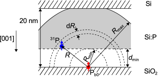
In the following we show that the time constant of the decay is a result of a distribution of 31P-P distances compatible with the width of the doped epilayer. To this end, we numerically calculate the exchange coupling as a function of the 31P-P distance . We further estimate the expected EDDEER decay by suitably averaging over the distribution of distances of the 31P-P ensemble. The geometry of the problem from the point of view of a dangling bond defect center P at the Si/SiO2 interface is shown in Figure 3. Phosphorus donors are located in the nm thick doped epilayer above the Si/SiO2 interface.
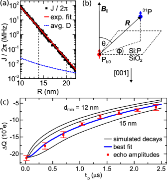
We calculate the exchange interaction with a Heitler-London approach Heitler and London (1927); Sugiura (1927) as the energetic difference of the singlet and triplet states. The ground-state wavefunction of the 31P electron located at is modeled as an isotropic hydrogen-like orbital
| (2) |
with the effective Bohr radius . The electron effective mass (with and ) and dielectric constant in the silicon crystal yield an effective Bohr radius nm Sze and Ng (2007). The Bloch character is not included in the simulations since its effect is averaged out for a random distribution of donors Koiller et al. (2001). The P wavefunction is mainly localized at the respective Si atom as confirmed by measurements of the hyperfine interaction with the nearest neighbour nuclei Stesmans et al. (1998). We therefore use a highly localized hydrogen-like orbital with an effective radius of half the Si-Si bond-length Å as a simplified model of the P wave function Hoehne et al. (2011). We calculate the exchange interaction as a function of solving the integrals numerically with Monte Carlo integration Press et al. (2007). The result shown in Figure 4 (a) (squares) can be described by an exponential decay with decay constant (red line). For comparison, we also plot the dipole-dipole coupling averaged over all spin pairs with a spin-spin distance with the 31P donors spin located on the surface of a hemisphere, described by the angle between the vector connecting the two spins and the magnetic field and the azimuth angle [see Figure 4 (b)] as a function of [blue dashed line in Figure 4 (a)], given by Jeschke (2002). The dipole-dipole coupling is much smaller than the exchange interaction for all distances nm, which corresponds to the thickness of the doped epilayer studied, and we therefore neglect its contribution to the 31P-P coupling.
We further calculate the expected EDDEER response by averaging the oscillations over a distribution of 31P-P distances
| (3) |
where is the pulsed EDMR echo amplitude for . The integration area shown in grey in Figure 3 is defined by two parameters, the distance from the Si/SiO2 interface and the radius around the P center. We assume a constant density of 31P donors within the 20 nm-thick epilayer for the average over all observed P centers, so that . If exceeds the width of the doped layer, the integration area is cut accordingly.
The integration boundaries and used in our model (Figure 3) are a consequence of several constraints concerning the conditions for which pEDMR signals can be observed. Most importantly, the spin allowed transition rate 1/ of electrons between 31P donors and P centers Dreher et al. (2012) is expected to depend on the distance between them Thomas et al. (1965). For spin pairs which are too close, the recombination time constant becomes shorter than the free evolution interval of the spin echo and, therefore, these spin pairs do not contribute to the EDDEER signal. For the EDDEER experiments shown above, s, so that spin pairs with s will not be observed. This lower bound of corresponds to a minimum distance between the recombination partners. The typical density of dangling bonds at the Si/SiO2 interface is 1012 cm-2 for a native oxide Pierreux and Stesmans (2002), corresponding to an average distance of 10 nm between the P centers. If the average P-P distance is smaller than , the overlap of the capture volumes will lead to an effective layer of thickness in which all 31P recombine so quickly that they are not observed in our experiment. As we will see below, this case indeed holds in our samples and we therefore use a minimum distance from the interface rather than a minimum distance from the considered center as a lower boundary for the integration interval. In contrast, for spin pairs with too large values of , the recombination time constants become so long that no recombination occurs during the measurement time interval given by the upper bound of 40 s of the box-car integration interval, so that spin pairs with s also do not contribute to the EDDEER signal resulting in a maximum spin-spin distance . The recombination time constants which are observed in the EDDEER experiment presented, therefore, span a range of more than one order of magnitude.
The experimentally observed decay [red squares in Figure 4 (c)] is best described by a simulation using Equation (3) for a distribution of 31P-P distances from nm to nm, as determined by a least-squares fit (blue line) with and as free parameters. This corresponds to an average over individual values of the exchange coupling MHz. For comparison, further simulations with ranging from 12 nm to 15 nm in steps of 1 nm and nm are shown as well demonstrating that the resulting decay is rather sensitive to variations in .
IV Discussion and conclusions
To further support our model, we estimate the dependence of on by assuming that the recombination process involves an electron tunneling process through a potential barrier between 31P and P. Using the WKB-method Cohen-Tannoudji et al. (1977) we estimate
| (4) |
where a barrier width corresponding to the 31P-P distance and flat bands have been assumed. A first estimate for the potential barrier could be meV, corresponding to the binding energy of an electron in the 31P donor Sze and Ng (2007), so that Equation (4) becomes Thomas et al. (1965). However, a comparison of the distances and and the variation of estimated for the EDDEER pulse sequence length and the upper boxcar integration bounds indicates a significantly lower barrier of about 20 meV if the recombination can indeed be described by a WKB-model. This significantly lower barrier suggests that a more realistic model of the tunneling process has to account for the Coulomb potential of the phosphorus donor and the binding energy of the dangling bond.
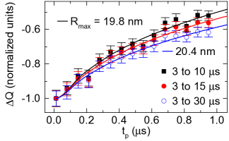
Using Equation (4), we can still obtain an estimate of the expected change of the upper bound of the observed range of 31P-P distances caused by a variation of the upper bound of the boxcar integration interval and compare it with experimental results. To this end, we recorded additional EDDEER decays for boxcar integration intervals ranging from 3 s to 10 s (full squares in Figure 5), 3 s to 15 s (full circles) and 3 s to 30 s (open circles), respectively, and fitted the results as described above. As expected, for an increase of the upper bound of the boxcar integration interval slower decays are observed corresponding to larger . We find that the respective EDDEER decays are best described by a simulation of the signals (solid lines) with nm, 20 nm and 20.4 nm in reasonable agreement with the variation of 1.4 nm estimated using Equation (4) with meV.
The total free evolution time of the spin echo is longer than the time of the spins Huebl et al. (2008), so that only a small subensemble of 2% of the spin pairs contributes to the EDDEER signal also taking into account above . However, we assume that the time of the P spins does not depend on the spin pair distance, so that for this subensemble the range of coupling constants is the same as for the whole spin pair ensemble. Indeed, shortening to s as in Figure 5 leads to essentially the same EDDEER decay time constant.
Based on EDMR experiments some estimates of the spin-spin distances have been reported in the literature. The range of exchange coupling constants found here corresponds well to previous estimates for spin pairs formed by 31P donors and radiation defects (SL1), where an upper bound of the 31P-SL1 distance of 20 nm has been reported Akhtar et al. (2011). The range of coupling constants also compares favorably to the upper bound of MHz for 31P-P spin pairs obtained by Lu et al. Lu et al. (2011). In contrast, a much smaller spin-spin distance of nm has been reported based on the observed 31P decoherence time induced by magnetic field fluctuation at the Si/SiO2 interface Paik et al. (2010). However, these authors have evaluated their experimental data with a model by de Sousa de Sousa (2007) and mention that not all requirements for the application of the model were met. Using our estimation of the exchange coupling, nm would correspond to GHz which is not compatible with the experimental data.
The results obtained here suggest a more systematic study of the EDDEER decay for samples with different thicknesses of the doped epilayer and, therefore, different distributions of exchange coupling requiring larger changes of the boxcar integration interval than presented in the proof-of-principle experiments presented here. Ultimately, a -doped layer of 31P donors McKibbin et al. (2009) could provide a much better defined coupling between the donors and the P defects.
To summarize, we have measured the exchange coupling between 31P donors and P defects at the Si/SiO2 interface using electrically detected DEER. We find that the measured EDDEER signal can be explained by a distribution of 31P-P coupling strengths resulting from a distribution of 31P-P distances over the observed spin ensemble. A simulation of the experimental signal with a numerical calculation of the exchange coupling allows us to understand the experimental results by a distribution of 31P-P distances ranging from 14 nm to 20 nm corresponding to an exchange coupling from kHz to MHz.
Acknowledgements
The work was supported by DFG (Grant No. SFB 631, C3 and Grant No. SPP 1601, Br 1585/8-1) and BMBF (Grant No. EPR Solar).
References
- Spaeth and Overhof (2003) J.-M. Spaeth and H. Overhof, Point Defects in Semiconductors and Insulators (Springer, Berlin, 2003).
- Lepine (1972) D. J. Lepine, Phys. Rev. B 6, 436 (1972).
- Brandt et al. (2004) M. S. Brandt, S. T. B. Goennenwein, T. Graf, H. Huebl, S. Lauterbach, and M. Stutzmann, phys. stat. sol. (c) 1, 2056 (2004).
- McCamey et al. (2006) D. R. McCamey, H. Huebl, M. S. Brandt, W. D. Hutchison, J. C. McCallum, R. G. Clark, and A. R. Hamilton, Appl. Phys. Lett. 89, 182115 (2006).
- Baker et al. (2012) W. Baker, K. Ambal, D. Waters, R. Baarda, H. Morishita, K. van Schooten, D. McCamey, J. Lupton, and C. Boehme, Nature Commun. 3, 898 (2012).
- Schnegg et al. (2012) A. Schnegg, J. Behrends, M. Fehr, and K. Lips, Phys. Chem. Chem. Phys. 14, 14418 (2012).
- Schmidt and Solomon (1966) J. Schmidt and I. Solomon, Compt. Rend. B 263, 169 (1966).
- Kaplan et al. (1978) D. Kaplan, I. Solomon, and N. Mott, J. Phys. Lett. (Paris) 39, 51 (1978).
- Kishimoto et al. (1981) N. Kishimoto, K. Morigaki, and K. Murakami, J. Phys. Soc. Jpn. 50, 1970 (1981).
- Stich et al. (1995) B. Stich, S. Greulich-Weber, and J.-M. Spaeth, J. Appl. Phys. 77, 1546 (1995).
- Hoehne et al. (2010) F. Hoehne, H. Huebl, B. Galler, M. Stutzmann, and M. S. Brandt, Phys. Rev. Lett. 104, 046402 (2010).
- Kane (1998) B. E. Kane, Nature 393, 133 (1998).
- Morello et al. (2010) A. Morello, J. J. Pla, F. A. Zwanenburg, K. W. Chan, K. Y. Tan, H. Huebl, M. Mottonen, C. D. Nugroho, C. Yang, J. A. van Donkelaar, A. D. C. Alves, D. N. Jamieson, C. C. Escott, L. C. L. Hollenberg, R. G. Clark, and A. S. Dzurak, Nature 467, 687 (2010).
- Boehme and Lips (2002) C. Boehme and K. Lips, phys. stat. sol. (b) 233, 427 (2002).
- de Sousa (2007) R. de Sousa, Phys. Rev. B 76, 245306 (2007).
- Stegner et al. (2006) A. R. Stegner, C. Boehme, H. Huebl, M. Stutzmann, K. Lips, and M. S. Brandt, Nature Phys. 2, 835 (2006).
- Huebl et al. (2008) H. Huebl, F. Hoehne, B. Grolik, A. R. Stegner, M. Stutzmann, and M. S. Brandt, Phys. Rev. Lett. 100, 177602 (2008).
- Dreher et al. (2012) L. Dreher, F. Hoehne, M. Stutzmann, and M. S. Brandt, Phys. Rev. Lett. 108, 027602 (2012).
- Lu et al. (2011) J. Lu, F. Hoehne, A. R. Stegner, L. Dreher, M. Stutzmann, M. S. Brandt, and H. Huebl, Phys. Rev. B 83, 235201 (2011).
- Milov et al. (1981) A. D. Milov, K. M. Salikhov, and M. D. Shirov, Sov. Phys. - Solid State 24, 565 (1981).
- Jeschke (2002) G. Jeschke, Macromol. Rapid Commun. 23, 227 (2002).
- Jeschke and Schweiger (2001) G. Jeschke and A. Schweiger, Principles of Pulse Electron Paramagnetic Resonance (Oxford University Press, Oxford, 2001).
- Klauder and Anderson (1962) J. R. Klauder and P. W. Anderson, Phys. Rev. 125, 912 (1962).
- Boehme and Lips (2003) C. Boehme and K. Lips, Phys. Rev. B 68, 245105 (2003).
- Hoehne et al. (2012) F. Hoehne, L. Dreher, J. Behrends, M. Fehr, H. Huebl, K. Lips, A. Schnegg, M. Suckert, M. Stutzmann, and M. S. Brandt, Rev. Sci. Instrum. 83, 043907 (2012).
- Stesmans and Afanas’ev (1998) A. Stesmans and V. V. Afanas’ev, J. Appl. Phys. 83, 2449 (1998).
- Feher (1959) G. Feher, Phys. Rev. 114, 1219 (1959).
- Heitler and London (1927) W. Heitler and F. London, Z. Phys. A 44, 455 (1927).
- Sugiura (1927) Y. Sugiura, Z. Phys. A 45, 484 (1927).
- Sze and Ng (2007) S. M. Sze and K. K. Ng, Semiconductor Devices: Physics and Technology (Wiley–Interscience, Hoboken, NJ, 2007).
- Koiller et al. (2001) B. Koiller, X. Hu, and S. Das Sarma, Phys. Rev. Lett. 88, 027903 (2001).
- Stesmans et al. (1998) A. Stesmans, B. Nouwen, and V. V. Afanas’ev, Phys. Rev. B 58, 15801 (1998).
- Hoehne et al. (2011) F. Hoehne, J. Lu, A. R. Stegner, M. Stutzmann, M. S. Brandt, M. Rohrmüller, W. G. Schmidt, and U. Gerstmann, Phys. Rev. Lett. 106, 196101 (2011).
- Press et al. (2007) W. H. Press, S. A. Teukolsky, W. T. Vetterling, and B. P. Flannery, Numerical Recipes: The Art of Scientific Computing (Cambridge University Press, Cambridge, 2007).
- Thomas et al. (1965) D. G. Thomas, J. J. Hopfield, and W. M. Augustyniak, Phys. Rev. 140, A202 (1965).
- Pierreux and Stesmans (2002) D. Pierreux and A. Stesmans, Phys. Rev. B 66, 165320 (2002).
- Cohen-Tannoudji et al. (1977) C. Cohen-Tannoudji, B. Diu, and F. Laloë, Quantum mechanics (Wiley, New York, 1977).
- Akhtar et al. (2011) W. Akhtar, H. Morishita, K. Sawano, Y. Shiraki, L. S. Vlasenko, and K. M. Itoh, Phys. Rev. B 84, 045204 (2011).
- Paik et al. (2010) S.-Y. Paik, S.-Y. Lee, W. J. Baker, D. R. McCamey, and C. Boehme, Phys. Rev. B 81, 075214 (2010).
- McKibbin et al. (2009) S. R. McKibbin, W. R. Clarke, A. Fuhrer, T. C. G. Reusch, and M. Y. Simmons, Appl. Phys. Lett. 95, 233111 (2009).