Transistor operation and mobility enhancement in top-gated LaAlO3 / SrTiO3 heterostructures
Abstract
We report the operation of LaAlO3 / SrTiO3 depletion mode top-gated junction field-effect transistors using a range of LaAlO3 thicknesses as the top gate insulator. Gated Hall bars show near ideal transistor characteristics at room temperature with on-off ratios greater than 1000. Lower temperature measurements demonstrate a systematic increase in the Hall mobility as the sheet carrier density in the channel is depleted via the top gate, providing a route to higher mobility, lower density electron gases in this system.
The electric field-effect has been successfully applied in a top-gate geometry to create normally-off transistors in undoped SrTiO3 (STO).Shibuya et al. (2004); Nakamura et al. (2006) Diverse properties have been studied including superconductivity,Ueno et al. (2008); Lee et al. (2011a) thermo-electricity,Ohta et al. (2010) Kondo physics,Lee et al. (2011b) and percolation effects.Li et al. (2012) The normally-on interface between LaAlO3 (LAO) and TiO2 terminated (100) STO Ohtomo and Hwang (2004) has also been electrostatically modulated from the back-side using the STO substrate as the gate dielectric.Thiel et al. (2006); Caviglia et al. (2008); Bell et al. (2009a); Ben Shalom et al. (2010); Caviglia et al. (2010); Joshua et al. (2012); Bert et al. (2012); Flekser et al. (2012); Kalisky et al. (2012) Although back-gating is rather robust and reliable, it simultaneously changes many parameters, most notably the confining electric field strength at the interface, Hall mobility and sheet carrier density.Bell et al. (2009a) Hence back-gating by itself does not allow low sheet carrier densities to be reached while maintaining relatively high Hall mobilities. Nor can the Rashba spin-orbit coupling be controlled independently of the sheet carrier density. Top-gating is a natural complimentary technique to tune the electronic properties: as is well-known in conventional semiconductor systems both the top- and back-gate geometries change the confining potential of the electron gas, but the spatial extent of the envelope electron wavefunction is altered in quite distinct ways for the two cases.Hirakawa et al. (1985)
The challenges of switching on devices at low temperatures with a top gate in STO,Nakamura et al. (2006) can be mitigated by using the depletion mode of junction gate field-effect transistors. Somewhat surprisingly however, given the attractively large band-gap of the over-layer in LAO/STO heterostructures, top-gate depletion devices have only recently been demonstrated by Förg et al.Förg et al. (2012) over a temperature range 173 K 373 K. These devices had a fixed LAO thickness, unit cells (uc), and short (20 m - 200 m) and wide (1600 m) channels, to enable device operation with a reduced channel resistance and gate leakage. However the two-probe device geometry prevented the determination of the sheet carrier density, , and hence the Hall mobility. Here we employed micrometer-scale Hall bars to enable precise Hall measurements, and study the field effect on the carrier density, for various . Ideal transistor operation with top-gating was demonstrated, as evidenced by the direct scaling of the mobile sheet carrier density obtained from the Hall effect with the expected modulation by the top-gate voltage, . A sheet carrier density modulation of up to cm-2 was achieved with in the range -1 V +1 V and 2 K 300 K. Notably, at lower temperatures the Hall mobility was significantly enhanced with field effect depletion of the electron gas, demonstrating the potential of top-gating to reach low sheet carrier density and high mobilities.
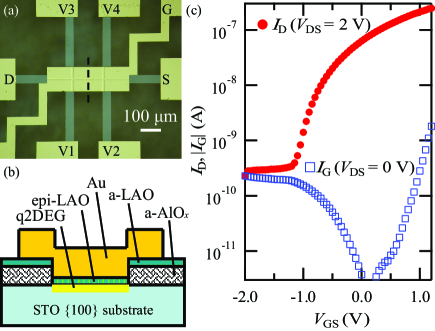
The LAO/STO heterostructures were fabricated by pulsed laser deposition on TiO2 terminated STO (100) substrates using a pre-deposited amorphous AlOx hard mask to define the Hall bar as described elsewhere.Bell et al. (2009a) The LAO thicknesses were in the range 4 uc 22 uc. The channel length covered by the gate was 400 m, and the channel width in the range m. The top electrode was formed using ex-situ sputtered Au with thickness nm, and the source and drain were contacted with Al ultrasonic wirebonding. Figure 1(a) and (b) shows an optical image of a typical device, showing the source, drain and gate contacts, together with a schematic device cross-section. All transport measurements were carried out with a semiconductor parameter analyzer in DC mode, and capacitance measurements were made using a LCR meter. When the devices were on, the gate leakage current was always significantly smaller than the drain current , an example of which is shown by the characteristics in Fig. 1(c). The gate leakage shows a similar form to previous studies.G. Singh-Bhalla et al. (2011)
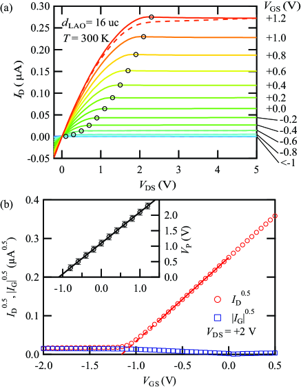
Clear normally-on transistor characteristics at K are shown in Fig. 2 for the case of uc. Pinch-off is observed for -0.8 V +1.2 V, with a clear saturation at higher . Differentiating these data to obtain the channel conductance , and extrapolating to zero , we find the pinch-off voltage as a function of , as shown in the inset of Fig. 2(b). The corresponding current at , , defines the co-ordinates for a fixed , as shown by the circles in Fig. 2(a). The threshold voltage could be obtained as V by fitting the data to the relationship .Sze (1985) Taking a transfer curve at a source-drain voltage of V, as shown in Fig. 2(b), essentially ideal quadratic form of is found, as expected from the gradual-channel model in the saturation regime.Sze (1985) These data allow a clear extrapolation of the threshold voltage as shown, giving V. The good agreement between these two values, obtained by two different analysis methods, suggests that the mobile carriers in the channel are ideally tuned by , with on-off current ratio’s of greater than 1000 being achievable. Small hysteresis could be observed between increasing and decreasing in the transfer characteristics, as shown for the case of V in Fig. 2(a), where the difference in between the increasing and decreasing sweep of is of the scale of 10 nA.
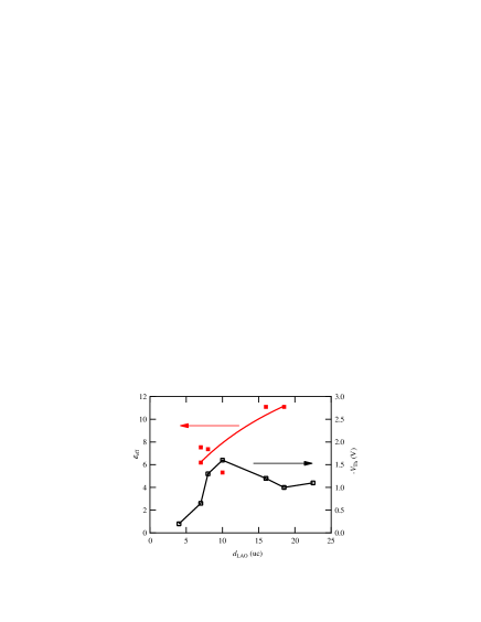
We systematically varied , and were able to achieve transistor operation over the thickness range 4 uc 22 uc. The scaling of is shown in Fig. 3. does not scale monotonically with , as would be the case for constant sheet carrier density, via the relation , here is the electronic charge, and are the vacuum and LAO relative permittivities respectively, and the sign convention is taken such that and . It is notable that a systematic variation of the transport properties has been seen in this thickness regime elsewhere.Bell et al. (2009b); Cancellieri et al. (2010); G. Singh-Bhalla et al. (2011) In order to more carefully examine this issue, we characterized several samples at lower temperatures where the Hall effect could be more reliably measured to directly measure the sheet carrier density change, and relate it to the capacitive character of the gate dielectric, since . Here the effective capacitance is modeled as a ‘dead’ layer with thickness and dielectric constant in series with a bulk-like LAO layer with dielectric constant . From a simple series capacitor model . We note that the dead layer thickness also includes possible suppression of the dielectric properties at the Au/LAO interface.Stengel and Spaldin (2006) Assuming otherwise ideal capacitor behavior, for various can be used to extract , and estimate , and . The measured is shown in Fig. 3, together with a theoretical fit which gives , and uc. These estimates, in particular the value of emphasize that the atomic scale nature of interface between the gate and the electron gas.
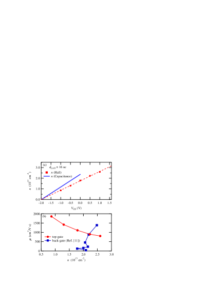
With the establishment of robust transistor operation at room temperature, it is important to consider if the top-gating geometry can be successfully applied at lower temperatures. Figure 4(a) shows clearly that can be ideally tuned with the top gate in a uc, m sample at K, where we compare the variation from the Hall effect to that predicted from the measured device capacitance (940 pF with top-gated channel area 0.0504 mm2) at V (solid line), assuming that cm-2 at V. Here the capacitance was measured in a frequency range of 20-100 Hz with an AC modulation voltage of 50 mV. In this range the loss tangent was and the gate leak conduction is negligibly small. In addition to the good agreement between the capacitance data and the Hall effect, as was depleted the Hall mobility showed a clear increase: the opposite tendency compared to back-gate field effect modulation,Bell et al. (2009a) as shown in Fig. 4(b).
The dramatic asymmetry in the mobility modulation between back- and top-gating can be understood by considering the action of the gate voltages on the confined electron gas. For negative back-gating the applied electric field tends to confine the electrons closer to the interface where they are scattered more strongly.Bell et al. (2009a) In the top gate geometry by contrast, the center of weight of the envelope wavefunction of the electron gas is pushed away from the interface as the electron gas is depleted and the self-consistent confining electric field is reduced.Hirakawa et al. (1985) This results in a local three-dimensional electron density that becomes smaller, and located in the less disordered bulk STO as , producing the observed enhancement of the Hall mobility as is decreased. The significance here is that the systematic suppression achieved by the top gate voltage can provide access to a regime with both smaller carrier density and less disorder (higher mobility), where other methods have experienced difficulties in approaching this regime. By combining the top-gate with an additional back-gate at low temperatures, we can also envisage independently tuning the sheet carrier density and Hall mobility to control the electronic character of this fascinating system.
The authors acknowledge support by the Department of Energy, Office of Basic Energy Sciences, Materials Sciences and Engineering Division, under contract DE-AC02-76SF00515. M. H. acknowledges partial support from the ONR-MURI number N00014-12-1-0976.
References
- Shibuya et al. (2004) K. Shibuya, T. Ohnishi, M. Lippmaa, M. Kawasaki, and H. Koinuma, Appl. Phys. Lett. 85, 425 (2004).
- Nakamura et al. (2006) H. Nakamura, H. Takagi, I. H. Inoue, Y. Takahashi, T. Hasegawa, and Y. Tokura, Appl. Phys. Lett. 89, 133504 (2006).
- Ueno et al. (2008) K. Ueno, S. Nakamura, H. Shimotani, A. Ohtomo, N. Kimura, T. Nojima, H. Aoki, Y. Iwasa, and M. Kawasaki, Nature Mater. 7, 855 (2008).
- Lee et al. (2011a) Y. Lee, C. Clement, J. Hellerstedt, J. Kinney, L. Kinnischtzke, X. Leng, S. D. Snyder, and A. M. Goldman, Phys. Rev. Lett. 106, 136809 (2011a).
- Ohta et al. (2010) H. Ohta, Y. Sato, T. Kato, S. Kim, K. Nomura, Y. Ikuhara, and H. Hosono, Nature Commun. 1, 118 (2010).
- Lee et al. (2011b) M. Lee, J. R. Williams, S. Zhang, C. D. Frisbie, and D. Goldhaber-Gordon, Phys. Rev. Lett. 107, 256601 (2011b).
- Li et al. (2012) M. Li, T. Graf, T. D. Schladt, X. Jiang, and S. S. P. Parkin, Phys. Rev. Lett. 109, 196803 (2012).
- Ohtomo and Hwang (2004) A. Ohtomo and H. Y. Hwang, Nature 427, 423 (2004).
- Thiel et al. (2006) S. Thiel, G. Hammerl, A. Schmehl, C. W. Schneider, and J. Mannhart, Science 313, 1942 (2006).
- Caviglia et al. (2008) A. Caviglia, S. Gariglio, N. Reyren, D. Jaccard, T. Schneider, M. Gabay, S. Thiel, G. Hammerl, J. Mannhart, and J.-M. Triscone, Nature 456, 624 (2008).
- Bell et al. (2009a) C. Bell, S. Harashima, Y. Kozuka, M. Kim, B. G. Kim, Y. Hikita, and H. Y. Hwang, Phys. Rev. Lett. 103, 226802 (2009a).
- Ben Shalom et al. (2010) M. Ben Shalom, M. Sachs, D. Rakhmilevitch, A. Palevski, and Y. Dagan, Phys. Rev. Lett. 104, 126802 (2010).
- Caviglia et al. (2010) A. D. Caviglia, M. Gabay, S. Gariglio, N. Reyren, C. Cancellieri, and J.-M. Triscone, Phys. Rev. Lett. 104, 126803 (2010).
- Joshua et al. (2012) A. Joshua, S. Pecker, J. Ruhman, E. Altman, and S. Ilani, Nature Commun. 22, 1129 (2012).
- Bert et al. (2012) J. A. Bert, K. C. Nowack, B. Kalisky, H. Noad, J. R. Kirtley, C. Bell, H. K. Sato, M. Hosoda, Y. Hikita, H. Y. Hwang, et al., Phys. Rev. B 86, 060503 (2012).
- Flekser et al. (2012) E. Flekser, M. Ben Shalom, M. Kim, C. Bell, Y. Hikita, H. Y. Hwang, and Y. Dagan, Phys. Rev. B 86, 121104(R) (2012).
- Kalisky et al. (2012) B. Kalisky, J. A. Bert, B. B. Klopfer, C. Bell, H. K. Sato, M. Hosoda, Y. Hikita, H. Y. Hwang, and K. A. Moler, Nature Commun. 3, 922 (2012).
- Hirakawa et al. (1985) K. Hirakawa, H. Sakaki, and J. Yoshino, Phys. Rev. Lett. 54, 1279 (1985).
- Förg et al. (2012) B. Förg, C. Richter, and J. Mannhart, Appl. Phys. Lett. 100, 053506 (2012).
- G. Singh-Bhalla et al. (2011) G. Singh-Bhalla, C. Bell, J. Ravichandran, W. Siemons, Y. Hikita, S. Salahuddin, A. F. Hebard, H. Y. Hwang, and R. Ramesh, Nature Phys. 7, 80 (2011).
- Sze (1985) S. M. Sze, Semiconductor devices, Physics and Technology (Wiley, 1985).
- Bell et al. (2009b) C. Bell, S. Harashima, Y. Hikita, and H. Y. Hwang, Appl. Phys. Lett. 94, 222111 (2009b).
- Cancellieri et al. (2010) C. Cancellieri, N. Reyren, S. Gariglio, A. D. Caviglia, A. Fête, and J.-M. Triscone, EPL 91, 17004 (2010).
- Stengel and Spaldin (2006) M. Stengel and N. A. Spaldin, Nature 443, 679 (2006).