Moiré minibands in graphene heterostructures with almost
commensurate hexagonal crystals
Abstract
We present a phenomenological theory of the low energy moiré minibands of Dirac electrons in graphene placed on an almost commensurate hexagonal underlay with a unit cell approximately three times larger than that of graphene. A slight incommensurability results in a periodically modulated intervalley scattering for electrons in graphene. In contrast to the perfectly commensurate Kekulé distortion of graphene, such supperlattice perturbation leaves the zero energy Dirac cones intact, but is able to open a band gap at the edge of the first moiré subbband, asymmetrically in the conduction and valence bands.
pacs:
73.22.Pr,73.21.Cd,72.80.VpTwo alternative methods exist to create long-period superlattices for two-dimensional (2D) electrons. One method, developed for semiconductors, is based on the lithographic patterning of the semiconductor surface semiconductor_superlattices . The other method, highlighted by the studies of 2D atomic crystals, arises naturally from the existence of quasi-periodic moiré patterns formed by two slightly incommensurate 2D lattices with similar crystal symmetry, placed on top of each other. Graphene on hexagonal boron nitride is one example of such heterostructure, where the effect of the moiré superlattice on 2D electrons leads to pronounced changes in the electronic properties detected by STM marchini_prb_2007 ; diaye_njp_2008 ; decker_nanolett_2011 , and magnetotransport experiments ponomarenko_nature_2013 ; dean_nature_2013 ; hunt_science_2013 .
The specific form of moiré superlattice for graphene electrons, generated by a hexagonal underlay, depends on the ratio between the periods of the two lattices and their mutual orientation. The abundance of layered hexagonal crystals and semiconductors with a hexagonal surface layer, allows for a multiplicity of qualitatively different superlattice structures, with various levels of moiré super-cell complexity. The simplest and, by now, best studied is the highly orientated graphene-hBN heterostructure. Here we analyze the second simplest moiré pattern for Dirac electrons in graphene produced by a hexagonal underlay with an elementary unit cell approximately 3 times bigger than that of graphene. The effect of a perfectly commensurate superlattice, known as the Kekulé distortion of the honeycomb lattice cheianov_ssc_2009 , consists in the Bragg type intervalley scattering of graphene electrons, which opens a gap between the conduction and valence bands. A hexagonal underlay with the lattice constant , , slightly different from that of the Kekulé superlattice of graphene and a small misaligned angle , produce a periodically oscillating intervalley coupling. Although this does not open a gap in graphene’s Dirac point, it creates a specific miniband spectrum, whose generic features are studied in this paper. Below, we employ a phenomenological approach to classify the possible structure of moiré minibands of Dirac electrons in graphene wallbank_prb_12 and, in particular, the behavior of the edge of the first minibands on the conduction and valence band sides.

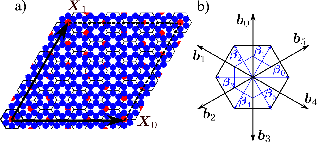
The image of a moiré supperlattice for graphene on a substrate with a period almost commensurate with the Kekulé lattice of graphene is shown in Fig. 1. Since graphene electrons belong to the Bloch states in its hexagonal Brillouin zone corners and a Kekulé perturbation leads to their intervalley Bragg scattering, the symmetry of the electronic system is described by the group of wavevectors , equivalent to the extended point group where is an elementary translation of the honeycomb lattice. That is why in Fig. 1 (a) we show both the actual positions of carbon atoms in graphene and, using lines, the Kekulé lattice. The periodic occurrence of sites from the underlay under equivalent positions of graphene honeycomb lattice is described by a moiré pattern which is periodic under translations by and . The associated reciprocal lattice vectors belong to the set where is the rotation matrix, and , so that . In contrast, the equivalent positions of substrate sites on the Kekulé lattice are characterized by the times longer period of and reciprocal lattice vectors from the set with . The coexistence of these two periodicities is taken into account, on an equal footing, in the phenomenological Hamiltonian for graphene’s Dirac electrons,
| (1) | |||
This Hamiltonian is written in terms of the Pauli matrices and which act separately on the sublattice and valley components of the 4-spinors describing graphene electrons. Hence, the second line describes intravalley Bragg scattering, whereas the first line accounts for intervalley scattering. In writing , we use the earlier observation yankowitz_natphys_2012 ; ortix_prb_2012 ; kindermann_prb_2012 ; wallbank_prb_12 ; twisted_blg_lopes_dos_santos ; twisted_blg_bistritzer that the potential felt by the graphene electrons is smoothened by the larger separation between graphene and the substrate than the carbon-carbon distance in graphene. For graphene on hBN, as well as twisted bilayer graphene, this resulted in the presence of only the simplest set of harmonics, , in the moiré perturbation yankowitz_natphys_2012 ; ortix_prb_2012 ; kindermann_prb_2012 ; wallbank_prb_12 ; twisted_blg_lopes_dos_santos ; twisted_blg_bistritzer . For graphene on a almost commensurate hexagonal underlay the same argument leads to the appearance of the intervalley terms. In Eq. (1), the relative strength of moiré perturbations, measured in the unit of energy , is set by dimensionless parameters , , , . Here, we assume that such moiré perturbation is small, , , and that the underlay has an inversion-symmetric unit cell, which is a natural approximation footnote:inversion for a simple monoatomic surface layer.
To supplement a phenomenological approach to describe the moiré supperlattice, Eq. (1), we also estimated parameter and for two limiting microscopic models: (a) the underlay is modeled as hexagonal lattice of point charges wallbank_prb_12 , and (b) the underlay is modeled as a lattice of atomic orbitals on to which the graphene electrons can hop (adapted from a model of twisted bilayer graphene kindermann_prb_2011 ). Both models produce similar estimates for sets of phenomenological parameters and ,
| (2) | |||
However model (a) predicts , whereas model (b) predicts footnote:model .
The features of the miniband spectrum of the Dirac electrons prescribed by the intravalley terms, , in the second line of Eq. (1) have already been explored in studies of graphene on hBN yankowitz_natphys_2012 ; ortix_prb_2012 ; kindermann_prb_2012 ; wallbank_prb_12 . The characteristic feature, present in the low energy graphene band structure for this case, consist in the formation of additional mini Dirac points yankowitz_natphys_2012 ; ortix_prb_2012 ; wallbank_prb_12 in a gapless spectrum. In contrast, intervalley perturbations , are able to open gaps in the spectrum at the edges of the low energy moiré minibands. Hence, we focus on the role of the intervalley terms, and explore the parameter space , classifying the resulting electron spectra. It is useful to notice that for the Hamiltonian in Eq. (1)
| (3) |
The first equality in Eq. (3) allows us to relate the bandstructure of the valence band to that of the conduction band by flipping the sign of . Also, it turns out that the parameter affects the miniband spectra of electrons only in the second order, since its first order effect on the electron energies can be removed by the gauge transformation .
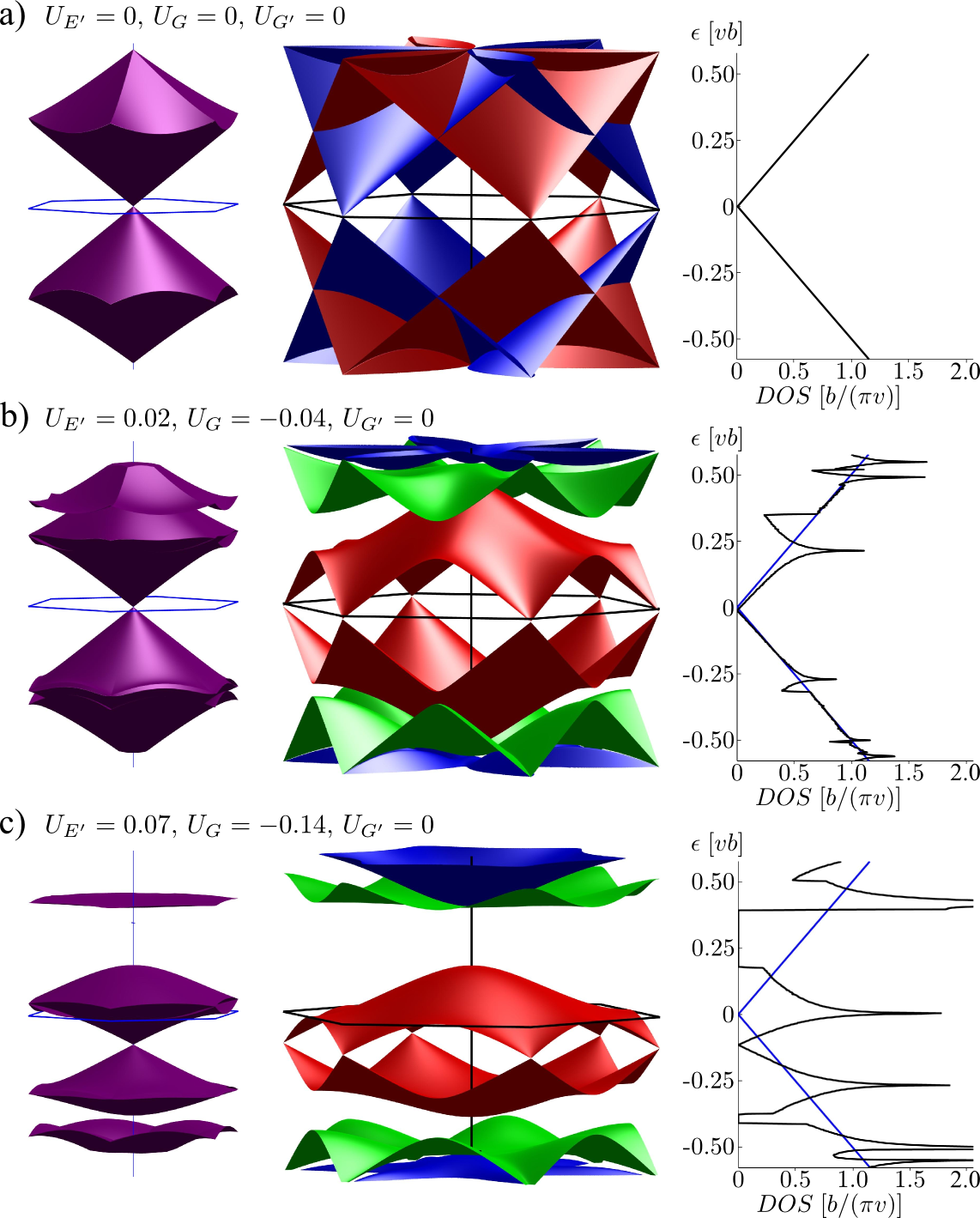
The correspondence between the translational symmetries of the Hamiltonian and the geometrical symmetry group of the moiré supperlattice, , is set by the fact that a translation e.g. by the period indicated in Fig. 1, is accompanied by a valley-dependent unitary gauge transformation, which represents the effect of the elementary translation of the honeycomb lattice on the 4-component spinors . This argument establishes the isomorphism of to the symmetry group of the Hamiltonian , where instead of geometrical translation we use (and instead of ). This correspondence allows one to use two equivalent descriptions of the folded mini Brillouin zone (mBZ) of the electrons in the presence of the moiré pattern, Fig. 1(b). One, based on the longer periodicity implicit in the dependence of the intervalley part of the Hamiltonian , suggests plotting the miniband dispersion over the smaller mBZ. The other, adjusted to the periodicity of the geometrical arrangement of atoms, uses the three times larger mBZ. For the smaller mBZ, the Dirac cones from both and valleys are folded onto the center of the mBZ, resulting in the valley degenerate dispersion surfaces shown in the left panel of Fig. 2(a). In contrast, the zone folding into the larger mBZ, shown in the center panel, places Dirac cones from graphene’s two valleys at opposite mBZ corners. The folding of dispersion surfaces from the larger mBZ into the smaller mBZ can be used relate the spectra shown in these alternative schemes. The unfolding of smaller mBZ into the larger mBZ is provided by the gauge transformation , where represents a valley dependent shift of momentum. After this gauge transformation, the new Hamiltonian can be written solely in terms of the harmonics,
| (4) | |||


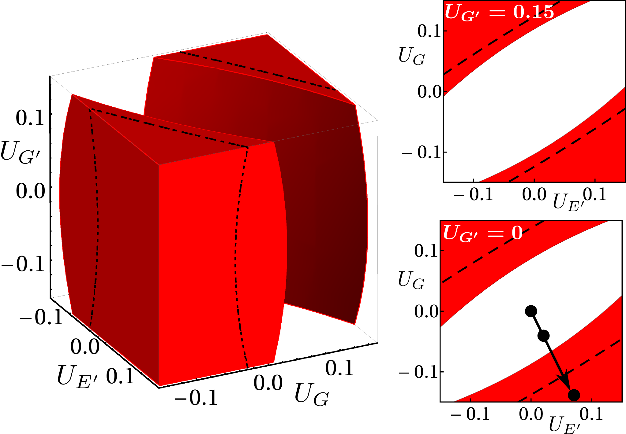
Characteristic miniband spectra, calculated by numerical diagonalization in the basis of zone-folded plane waves of and Dirac electrons, are shown in Fig. 2(b,c). The choices of phenomenological parameters used to calculate these spectra, marked with black dots in the lower right panel of Fig. 3, correspond to the direction in the parameter space set by Eq. (2) with . Since nesting obscures some of the dispersion branches, it is useful to plot them over both the smaller mBZ (left) and the larger mBZ (middle). Also, we note that, the calculated spectra will be electron-hole asymmetric, , unless either or .
Generically, we find either a gapped edge of the first moiré miniband (on the conduction and/or valence band side of the graphene spectra) for a strong moiré perturbation, or gapless spectra with overlapping minibands for a weak moiré perturbation. In all cases, the main Dirac point is preserved with a renormalized Dirac velocity, . The parameter range where the spectrum has a gap at the first miniband edge in the conduction band is shown in red in Fig. 3, whereas the parameter range with a gapless spectrum is left transparent. The magnitude of the band gap between the first and second minibands in either the conduction band () or the valence band (), may be expressed in the form
| (5) | |||
where and are the values of the indirect and direct band gaps. A negative value of indicates that the bands are overlapping (no band gap, transparent volume of Fig. 3).
| Substrate | [Å] | Structure | Ref |
|---|---|---|---|
| 4.03 | layered | furuseth_acta_1965 | |
| 4.04 | layered | wilson_api_1969 | |
| 4.05 | layered | mccanny_ssp_1966 | |
| 4.01-4.06 | layered | zolyomi_prb_2013 ; semiletov_sovphys_1964 ; gillan_chemmater_1997 | |
| 4.15 | (111) surface | Madelung_1991 | |
| 4.28 | (111) surface | Madelung_1991 | |
| 4.31 | (111) surface | Madelung_1991 | |
| 4.34 | (111) surface | Madelung_1991 | |
| graphene | 4.26 | Castro_Neto_RevModPhys_2009 |
To conclude, there are numerous substrates with surfaces that are almost commensurate with the Kekulé superlattice in graphene (Table 1). A sufficiently strong moiré perturbation for the Dirac electrons in graphene, placed at a small misalignment angle on such surfaces, results in a band gap between the first and second moiré minibands, on either the conduction or valence band side of graphene’s band structure, at energies . These band gaps may be either indirect (if the phenomenological parameters lie within the red volume of Fig. 3 between the black dashed lines), or direct (outside the black dashed lines). This observation suggests a new possibility to tailor electronic properties of graphene.
This work has been supported by EPSRC DTC NOWNANO, ERC Advanced Grant Graphene and Beyond, Royal Society Wolfson Research Merit Award, and EPSRC Science and Innovation Award.
References
- (1) D. K. Ferry, Prog. Quant. Electr. 16, 251 (1992); C. Albrecht, J. H. Smet, D. Weiss, K. von Klitzing, R. Hennig, M. Langenbuch, M. Suhrke, U. Rössler, V. Umansky, H. Schweizer, Phys. Rev. Lett. 83, 2234 (1999); T. Schlösser, K. Ensslin, J. P. Kotthaus, M. Holland, Europhys. Lett. 33, 683 (1996); C. Albrecht, J. H. Smet, K. von Klitzing, D. Weiss, V. Umansky, and H. Schweizer, Phys. Rev. Lett. 86, 147 (2001); M. C. Geisler, J. H. Smet, V. Umansky, K. von Klitzing, B. Naundorf, R. Ketzmerick, and H. Schweizer, Phys. Rev. Lett. 92, 256801 (2004).
- (2) S. Marchini, S. Günther, and J. Wintterlin, Phys. Rev. B 76, 075429 (2007).
- (3) A. T. N’Diaye , J. Coraux, T. N. Plasa, C. Busse and T. Michely, New J. Phys. 10, 043033 (2008).
- (4) R. Decker, Y. Wang, V. W. Brar, W. Regan, H. Tsai, Q. Wu, W. Gannett, A. Zettl, and M. F. Crommie, Nano Lett. 11, 2291 (2011).
- (5) L. A. Ponomarenko, R. V. Gorbachev, G. L. Yu, D. C. Elias, R. Jalil, A. A. Patel, A. Mishchenko, A. S. Mayorov, C. R. Woods, J. R. Wallbank, M. Mucha-Kruczynski, B. A. Piot, M. Potemski, I. V. Grigorieva, K. S. Novoselov, F. Guinea, V. Fal’ko and A. K. Geim, Nature 497, 594 (2013).
- (6) C. R. Dean, L. Wang, P. Maher, C. Forsythe, F. Ghahari, Y. Gao, J. Katoch, M. Ishigami, P. Moon, M. Koshino, T. Taniguchi, K. Watanabe, K. L. Shepard, J. Hone, P. Kim, Nature 497, 598 (2013).
- (7) B. Hunt, J. D. Sanchez-Yamagishi, A. F. Young, M. Yankowitz, B. J. LeRoy, K. Watanabe, T. Taniguchi, P. Moon, M. Koshino, P. Jarillo-Herrero, R. C. Ashoori, To appear in Science (2013).
- (8) V. V. Cheianov , V. Fal’ko , O. Syljuåsen , B. L. Altshuler, Sol. St. Commun. 149, 1499 (2009).
- (9) J. R. Wallbank, A. A. Patel, M. Mucha-Kruczynski, A. K. Geim, V. Fal’ko, Phys. Rev. B 87, 245408 (2013).
- (10) M. Yankowitz, J. Xue, D. Cormode, J. D. Sanchez-Yamagishi, K. Watanabe, T. Taniguchi, P. Jarillo-Herrero, P. Jacquod, and B. J. LeRoy, Nature Phys. 8, 382 (2012).
- (11) C. Ortix, L. Yang, and J. van den Brink, Phys. Rev. B 86, 081405 (2012).
- (12) M. Kindermann, B. Uchoa, D. L. Miller, Phys. Rev. B 86, 115415 (2012).
- (13) J. M. B. Lopes dos Santos, N. M. R. Peres, and A. H. Castro Neto, Phys. Rev. Lett. 99, 256802 (2007); Phys. Rev. B 86, 155449 (2012).
- (14) R. Bistritzer and A. H. MacDonald, Phys. Rev. B 81, 245412 (2010); 84, 035440 (2011).
- (15) Inversion asymmetric terms may be included into Eq. (1) by adding terms with and .
- (16) M. Kindermann and P. N. First, Phys. Rev. B 83, 045425 (2011).
-
(17)
For the point charge model wallbank_prb_12 ,
, ,
Here is the charge per substrate lattice site, the graphene-substrate distance, the electric permittivity and the Fourier transform of the graphene Pz orbitals. For the hoping model with the hopping integral to the substrate and is the energy of the substrate state. - (18) S. Furuseth, K. Selte, and A. Kjeksiius, Acta chem. scand. 19, 257. (1965).
- (19) J. A. Wilson and A. D. Yoffe, Advances in Physics 18, 193 (1969).
- (20) J. V. McCanny and R. B. Murray, J. Phys. C: Solid State Phys. 10, 1211 (1977).
- (21) V. Zólyomi, N. D. Drummond, and V. Fal’ko, Phys. Rev. B 87, 195403 (2013).
- (22) S. A. Semiletov and V. A. Vlasov, Sov. Phys. Crystallogr. 8, 704 (1964).
- (23) E. G. Gillan and A. R. Barron, Chem. Mater. 9, 3037 (1997).
- (24) O. Madelung (editor), Semiconductors: Group IV Elements and III-V Compounds in the series Data in Science and Technology, Springer-Verlag Berlin 1991.
- (25) A. H. Castro Neto, F. Guinea, N. M. R. Peres, K. S. Novoselov and A. K. Geim, Rev. Mod. Phys. 81, 109 (2009).