Also at ]Novosibirsk State University.
Transport properties of a 3D topological insulator
based on a strained
high mobility HgTe film
Abstract
We investigated the magnetotransport properties of strained, 80 nm thick HgTe layers featuring a high mobility of cm2/Vs. By means of a top gate the Fermi-energy is tuned from the valence band through the Dirac type surface states into the conduction band. Magnetotransport measurements allow to disentangle the different contributions of conduction band electrons, holes and Dirac electrons to the conductivity. The results are in line with previous claims that strained HgTe is a topological insulator with a bulk gap of 15 meV and gapless surface states.
- PACS numbers
-
73.25.+i, 73.20.At, 73.43.-f
pacs:
1pacs:
2pacs:
3pacs:
1The discovery of two (2D)- and three-dimensional (3D) topological insulators (TI), a new material class with insulating bulk and topologically protected, conducting surface states, has opened a new and exciting research field in condensed matter physics Kane and Mele (2005a, b); Bernevig and Zhang (2006); Bernevig et al. (2006); Fu and Kane (2007); Fu et al. (2007); Hsieh et al. (2008); Xia et al. (2009); Hasan and Kane (2010); Qi and Zhang (2011). Although quite a number of different, especially Bi based materials Checkelsky et al. (2009); Taskin and Ando (2009); Qu et al. (2010); Kim et al. (2012), belong to this category, materials which combine high charge carrier mobility and insulating bulk are still scarce. This is mostly due to the fact that Bi-based 3D TIs are heavily-doped alloy films with a very low mobility 1000 cm2/Vs and a high bulk carrier density of 1017 - 1019 cm-3. HgTe based 2D TI, on the other hand, are characterized by very high mobilities enabling the discovery of the quantum spin Hall effect Konig et al. (2007). A recent analysis of the sequence of quantum Hall plateaus suggests that also strained HgTe layers constitute a 3D TI. The strain opens a gap in the gapless semimetal HgTe, so that the TI properties can be explored by tuning the Fermi energy into the bulk gap and probing the transport properties of the gapless surface states. Although the strained HgTe film has a much higher mobility cm2/Vs, the high bulk carrier density and the absence of a top gate has complicated the detection of the 3D TI so far Brune et al. (2011); Olshanetsky et al. (2011).
The strain in HgTe layers, grown by molecular beam epitaxy (MBE), stems from a 0.3% lattice mismatch between HgTe and CdTe. The corresponding critical film thickness for pseudomorphic growth is larger than 100 nm meaning that thinner films adopt the substrate lattice constant. Due to this strain a small gap of meV opens (see below) in the bulk energy spectrum of the film. Within the bulk gap the gapless surface states reside. The charge neutrality point of the corresponding Dirac cone is located in the valence band Brune et al. (2011). Thus Dirac electrons with higher energy dominate electrical transport if the Fermi energy is located in the bulk gap. This allows us to map the bandstructure in the vicinity of the bulk gap by magnetotransport experiments as is outlined below.
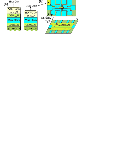
In this Letter we report on the transport properties of high mobility, 80 nm wide, strained HgTe films equipped with a gate. The low disorder, manifested in high charge carrier mobilities, together with the possibility to tune the Fermi energy from the valence via the gap into the conduction band, enables us to probe the 2D Dirac surface states when the Fermi energy is in the energy gap of the bulk. Since HgTe films grown on CdTe suffer from dislocations due to the lattice mismatch, our 80 nm thick HgTe films were separated from the CdTe substrate by a 20 nm thin Cd0.7Hg0.3Te buffer layer. This buffer layer increases the electron mobility by an order of magnitude (up to cm2/Vs) and reduces the bulk impurity concentration to values of order 1016 cm-3 (see supplemental material). We fabricated and investigated two types of devices: one with the upper HgTe surface uncapped and the other one covered with a 20 nm Cd0.7Hg0.3Te cap layer (see Fig. 1(a) and supplement). Since all measured major properties (magnetotransport traces, bulk energy gap etc.) of capped and uncapped films were found to be similar, we will only focus on the uncapped HgTe film below. For transport measurements the films were patterned into Hall bars supplied with top gates. Cross-sections of the devices are sketched in Fig. 1(a). Each Hall bar consists of three 50 m wide segments of different lengths (100, 250, and 100 m) with eight voltage probes. Ohmic contacts to the active layer were formed by alloying indium. For gating two types of dielectric layers were used, giving similar results: 100 nm SiO2 and 200 nm of Si3N4 grown by plasma chemical vapor deposition of SiH4 + N2O at 100∘C or 80 nm Al2O3 grown by atomic layer deposition. In both cases TiAu was deposited as metallic gate. Magnetotransport measurements were performed at temperatures between 1.5 K and 15 K and in magnetic fields up to 10 T. Several devices from the same wafer have been studied.
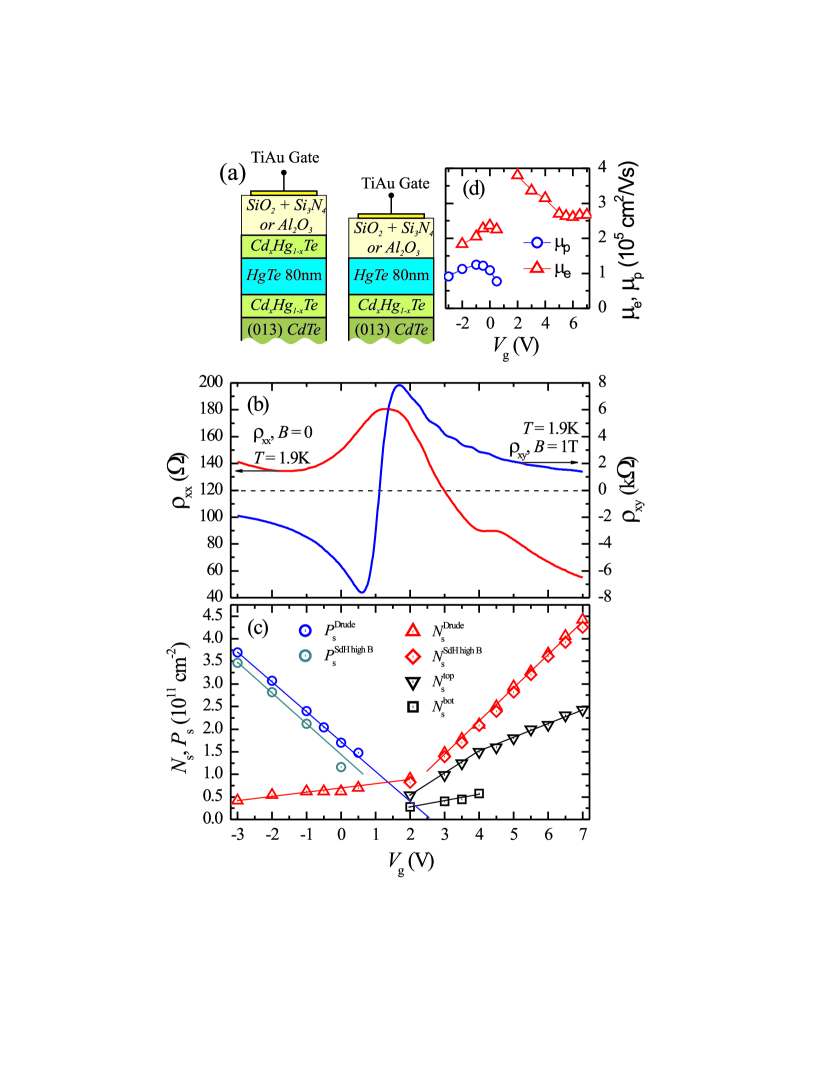
Fig. 1(b) shows the typical resistivity at and Hall resistance at T as a function of gate voltage at K for a HgTe film with Si3N4 insulator. The trace exhibits a maximum near V and is asymmetric with respect to the gate voltage: the resistance on the left hand side of the maximum is significantly higher than on the right side. While displays a maximum in Fig. 1(b), , taken at 1 T, changes sign at the same V. This suggests that the Fermi level can be tuned, as a function of , from the conduction band to the valence band.
For V the Fermi level is in the valence band, where according to band structure calculations (ref. Brune et al. (2011), supplement), holes and Dirac electrons coexist. The coexistence of two types of charge carriers is experimentally supported by a large positive magnetoresistance and by a non-linear , typical for electron-hole systems Blatt (1968); Kvon et al. (2008). To estimate mobility and density of the coexisting electron and holes we used the Drude formalism for two types of carriers. The total conductivity and Hall conductivity is given by the sum of electron and hole contributions to the conductivity. After tensor inversion one obtains expressions for and which can be fitted to the experimental data at each value. Examples are given in the supplement. A similar analysis to extract densities and mobilities of the two carrier species has been employed previously in semimetallic HgTe quantum wells Kvon et al. (2008). At V the non-linear Hall effect turns into an essentially linear dependence of indicating that the current is carried by only one sort of charge carriers, i.e. surface electrons. A remaining small non-linearity of is due to different densities and mobilties of these electrons on top and bottom surface.
The resulting electron and hole 2D density and mobility are presented in Fig. 1(c) (labeled as ”Drude”) and (d) 111Note that the experiment delivers averages over both surfaces and, in certain voltage regions, also over part of the bulk. This can be seen from the band scheme (Fig. S5, supplement) which shows the position of at different . Both, electron and hole densities change with by a factor of nearly 10, thus indicating that only a small concentration of bulk impurities contributes to the conductivity. Fig. 1(d) shows that electrons and holes exhibit very high mobilities exceeding cm2/Vs. The maximum electron mobility of cm2/Vs is an order of magnitude higher than in strained HgTe films discussed previously Brune et al. (2011); Olshanetsky et al. (2011) and almost a thousand times higher than in 3D Bi TI samples. Linear extrapolation of the data in Fig. 1(c) gives an intercept at V, suggesting that the valence band filling starts around here. At about the same value of the slope of in Fig. 1(c) and the temperature dependence of , shown in Fig. 2(a), change noticeably: For V does hardly change with but changes dramatically for V where varies by a factor 2 between K and 15 K. This behavior is ascribed to strong Landau scattering Gantmakher and Levinson (1987) of coexisting electron and hole states, similar to the one observed in Olshanetsky et al. (2009).
Another feature in emerges at V (Fig. 1(b)), accompanied by a change of the slope of (Fig. 1(c), extracted from low-field Shubnikov-de Haas (SdH) oscillations (see below). We suggest that this features mark the gate voltage at which the Fermi level starts to enter the conduction band. Therefore, the data presented in Fig. 1 and Fig. 2a imply that the gap opens between and V (top of valence band) and closes around V (bottom of conduction band). Then only Dirac states localized at the two surfaces of the strained 80 nm HgTe film contribute to transport. Outside this region Dirac electrons and bulk electrons (holes) conduct in parallel. A sketch of the corresponding density of states versus energy is shown in the inset of Fig. 2(a). Using the electron densities extracted at and and the calculated k-linear dispersion of Dirac electrons Brune et al. (2011) we estimate a gap size of meV. This value is very close to the one calculated in Brune et al. (2011) for a strained HgTe film. The same value we found for the Cd0.7Hg0.3Te capped HgTe film, indicating that the surface states are not affected by the precise nature of the interface.
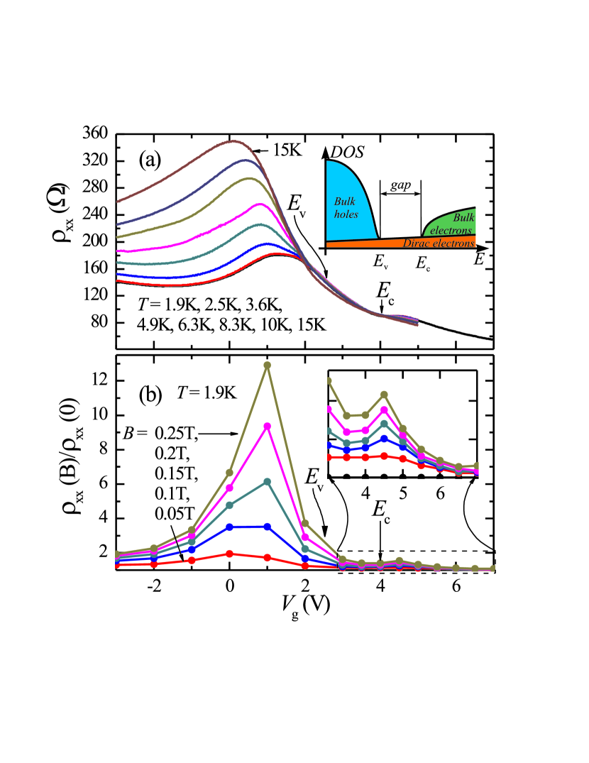
To check the validity of our picture further we resort to magnetoresistance measurements in a perpendicular magnetic field, displayed in Fig. 2(b). The magnetoresistance (MR) within classical Drude theory for two groups of carriers (labeled by index 1 and 2) is, for small fields, proportional to . Its magnitude, normalized to is proportional to , where and are conductivity and mobility of the respective carrier species at . The sign between depends on the carriers’ polarity: in case the carriers have the same polarity (e.g. Dirac electrons in the conduction band) the ”-” sign applies while in the case of different polarity (electrons and holes coexist) the mobilities add, thus resulting in a strong MR. Hence the maximum of the MR magnitude is expected to occur in the semimetal state with the Fermi level residing in the valence band near the charge neutrality point, where and and become comparable. A significant change of the MR magnitude is expected when the Fermi energy moves from the valence band into the gap where only Dirac electrons reside. For this single carrier type the MR is small. Corresponding normalized and data, displayed in Fig. 2(b), are in accord with this expectation. For V a large parabolic MR is observed with a pronounced MR maximum at V. In contrast, for V, i.e. where Dirac electrons prevail, the MR drops by a factor of up to 10. The MR is expected to rise again when the Fermi level moves from the gap into the conduction band, as two (or more) groups of carriers with different mobility are involved, i.e. Dirac and bulk electrons. Bulk electrons near the bottom of the conductance band are expected to have a much lower mobility than Dirac electrons. A corresponding increase is indeed visible in Fig. 2(b) (marked by ””).
Important extra information can be obtained from experiments in quantizing magnetic fields. SdH oscillations and quantized Hall steps can be seen in Fig. 3(a) as a function of for T. The maximum in at V corresponds to the charge neutrality point at which the Hall resistance (voltage) changes sign. On the left hand side, where low mobility holes dominate, no quantum Hall steps appear. In contrast, on the right hand side where Dirac fermions and conduction band electrons prevail, quantized Hall steps develop.
Surprisingly, the Hall steps extend into a region where conduction band and Dirac electrons coexist. The electron density, extracted from high-field SdH oscillations, plotted in Fig. 1(c), is identical to the one obtained from classical Drude fits. This means that the filling factors at high -fields are determined by the total electron concentration , i.e. bulk and surface electrons. Similarly, at large negative and high , the hole density extracted from SdH oscillations and from Drude theory are nearly equal, while at smaller bias the SdH data deliver smaller hole densities. This suggests that the filling factor in the valence band is given by the difference of bulk hole and surface electron density. This is similar to the situation observed in GaSb/InAs heterojunctions where electrons and holes coexist Mendez et al. (1985). A central observation is thus that bulk (which in our case is a 80 nm wide HgTe quantum well) and surface charge carriers determine jointly the high- LL filling factors. The minima do not vanish indicating parallel conduction probably due to the sides of the HgTe layer, which are oriented parallel to the applied magnetic field Brune et al. (2011). The quantized Hall steps on the electron side display, as in Brüne’s work Brune et al. (2011), even and odd integer plateau values, thus indicating different carrier densities for top and bottom surface.
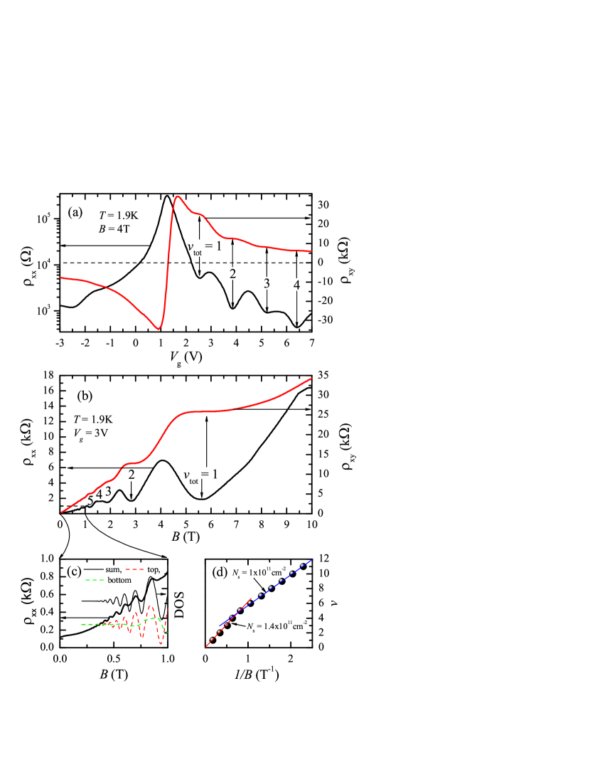
This is not surprising as it is a consequence of screening, i.e., a part of the electric field gets screened by the top layer of Dirac electrons. Applying an electric field to the top gate hence results in different filling rates . These rates can be easily estimated if is in the gap, i.e. between V and V. Then the change of top and bottom electron density is given by Luryi (1988) , where is the density of states of Dirac electrons on the top surface, and and are thickness and dielectric constant of the HgTe layer, respectively. Inserting typical values we obtain . Below we show that the experimentally observed difference in top and bottom layer filling rate is close to this expected value. Besides we plot in Fig. 1(c) also the electron density of the top surface as a function of . The corresponding data are obtained from the following consideration: Assuming that the carrier densities are equal at the flat band condition, i.e. at V, the electron density on the top surface becomes significantly higher for V. The higher carrier density of the top surface is expected to be connected with a higher electron mobility 222Comparison of CdHgTe capped and uncapped heterostructures (see supplement for details) proves that they have the same average mobility for in the gap. We thus conclude that for the same carrier density mobilities on top and bottom surface are approximately the same. This offers an opportunity to separate the electron density of top and bottom layer experimentally. As the higher mobility of the top layer is connected to a smaller Landau level broadening, Shubnikov de Haas oscillations commence at lower magnetic fields and dominate the low field magnetoresistance oscillations in Fig. 3(c). This is reflected in different periods of SdH oscillations in low and high -fields, displayed in Fig. 3(d). The positions of the SdH minima vs. filling factors can be fitted by two straight lines corresponding to the carrier density cm-2 of the top layer and the total carrier density cm-2. , extracted from low-field SdH-oscillations for different is shown in Fig. 1(c). In both cases we assumed spin-resolved LLs. The reduced slope of for V is a clear signature that moves in the conduction band. Since is constant, decreases when the bulk electron density starts to appear, i.e., when . For T Landau quantization gets resolved in the lower mobility bottom layer, too and, due to electron redistribution, the two surfaces (and for V also the bulk electrons) act like a single 2DEG with density . The redistribution of electrons in the TI state is possible via contacts, ungated conducting regions and via side facets of the HgTe film.
With , acquired from high-field SdH oscillations, and we can, for between V V, i.e. in the TI regime, calculate the carrier density of the bottom layer, . Corresponding data are also shown in Fig. 1(c). The slope of is by a factor of higher than the one of . This is in line with the effect of screening, discussed above.
In summary we have shown that an analysis of magnetotransport data in strained high-mobility HgTe layers brings out the different carrier types contributing to transport at different Fermi level positions. A strong magnetoresistance, observed in the valence band where electrons and holes coexist, is absent in the gap where only surface electron contribute, and rises again when the Fermi energy enters the conduction band. An analysis of high- and low-field quantum oscillations highlights the interplay of the different carrier types and allows to probe the carrier density of top and bottom layer in the TI regime separately.
Authors acknowledge the assistance of C. Linz in Al2O3 insulator and gate fabrication. This work was supported by the German Science Foundation (DFG) via Research Unit 1483 and SPP 1666, by the International Bureau of the German Federal Ministry of Education and Research (RUS 09/29), the Russian Foundation for Basic Research, and the Russian Academy of Sciences (Physics and Technology of Nanostructures Program).
References
- Kane and Mele (2005a) C. L. Kane and E. J. Mele, Phys. Rev. Lett. 95, 146802 (2005a).
- Kane and Mele (2005b) C. L. Kane and E. J. Mele, Phys. Rev. Lett. 95, 226801 (2005b).
- Bernevig and Zhang (2006) B. A. Bernevig and S.-C. Zhang, Phys. Rev. Lett. 96, 106802 (2006).
- Bernevig et al. (2006) B. A. Bernevig, T. L. Hughes, and S.-C. Zhang, Science 314, 1757 (2006).
- Fu and Kane (2007) L. Fu and C. L. Kane, Phys. Rev. B 76, 045302 (2007).
- Fu et al. (2007) L. Fu, C. L. Kane, and E. J. Mele, Phys. Rev. Lett. 98, 106803 (2007).
- Hsieh et al. (2008) D. Hsieh, D. Qian, L. Wray, Y. Xia, Y. S. Hor, R. J. Cava, and M. Z. Hasan, Nature 452, 970 (2008).
- Xia et al. (2009) Y. Xia, D. Qian, D. Hsieh, L. Wray, A. Pal, H. Lin, A. Bansil, D. Grauer, Y. S. Hor, R. J. Cava, and M. Z. Hasan, Nature Physics 5, 398 (2009).
- Hasan and Kane (2010) M. Z. Hasan and C. L. Kane, Rev. Mod. Phys. 82, 3045 (2010).
- Qi and Zhang (2011) X.-L. Qi and S.-C. Zhang, Rev. Mod. Phys. 83, 1057 (2011).
- Checkelsky et al. (2009) J. G. Checkelsky, Y. S. Hor, M.-H. Liu, D.-X. Qu, R. J. Cava, and N. P. Ong, Phys. Rev. Lett. 103, 246601 (2009).
- Taskin and Ando (2009) A. A. Taskin and Y. Ando, Phys. Rev. B 80, 085303 (2009).
- Qu et al. (2010) D.-X. Qu, Y. S. Hor, J. Xiong, R. J. Cava, and N. P. Ong, Science 329, 821 (2010).
- Kim et al. (2012) D. Kim, S. Cho, N. P. Butch, P. Syers, K. Kirshenbaum, S. Adam, J. Paglione, and M. S. Fuhrer, Nature Physics 8, 459 (2012).
- Konig et al. (2007) M. Konig, S. Wiedmann, C. Brune, A. Roth, H. Buhmann, L. W. Molenkamp, X.-L. Qi, and S.-C. Zhang, Science 318, 766 (2007).
- Brune et al. (2011) C. Brune, C. X. Liu, E. G. Novik, E. M. Hankiewicz, H. Buhmann, Y. L. Chen, X. L. Qi, Z. X. Shen, S. C. Zhang, and L. W. Molenkamp, Phys. Rev. Lett. 106, 126803 (2011).
- Olshanetsky et al. (2011) E. B. Olshanetsky, Z. D. Kvon, S. S. Kobylkin, D. A. Kozlov, N. N. Mikhailov, S. A. Dvoretskii, and J. C. Portal, JETP Lett. 93, 526 (2011).
- Blatt (1968) F. J. Blatt, Physics of Electronic Conduction in Solids (McGRAW-HILL BOOK COMPANY, 1968).
- Kvon et al. (2008) Z. D. Kvon, E. B. Olshanetsky, D. A. Kozlov, N. N. Mikhailov, and S. A. Dvoretskii, JETP Lett. 87, 502 (2008).
- Note (1) Note that the experiment delivers averages over both surfaces and, in certain voltage regions, also over part of the bulk. This can be seen from the band scheme (Fig. S5, supplement) which shows the position of at different .
- Gantmakher and Levinson (1987) V. F. Gantmakher and Y. B. Levinson, Carrier Scattering in Metals and Semiconductors (North-Holland Physics Publishing, Amsterdam, 1987).
- Olshanetsky et al. (2009) E. B. Olshanetsky, Z. D. Kvon, M. V. Entin, L. I. Magarill, N. N. Mikhailov, I. O. Parm, and S. A. Dvoretsky, JETP Lett. 89, 290 (2009).
- Mendez et al. (1985) E. E. Mendez, L. Esaki, and L. L. Chang, Phys. Rev. Lett. 55, 2216 (1985).
- Luryi (1988) S. Luryi, Appl. Phys. Lett. 52, 501 (1988).
- Note (2) Comparison of CdHgTe capped and uncapped heterostructures (see supplement for details) proves that they have the same average mobility for in the gap. We thus conclude that for the same carrier density mobilities on top and bottom surface are approximately the same.
Supplemental material for “Transport properties of a 3D topological insulator based on a strained high mobility HgTe film”
D. A. Kozlov, Z. D. Kvon, D. Weiss, E. B. Olshanetsky, N. N. Mikhailov, S. A. Dvoretsky
I Samples details
I.1 Heterostructure and Hall bar
We fabricated and investigated several devices based on two types of heterostructures. Both types were grown grown by molecular beam epitaxy on a (013)-oriented CdTe substrate and have very similar structure: the essential part is a strained 80 nm thick HgTe film (Fig. S1(a)). The two heterostructures types differ in the top layer sequence: in the first structure (named ”uncapped”) the HgTe is uncapped on top while the second one (”capped”) is covered with a 20 nm Cd0.7Hg0.3Te cap layer. Since HgTe films grown on CdTe suffer from dislocations due to lattice mismatch, thus causing low mobility ( cm2/Vs) and high impurity concentration ( cm-3) in the bulk Brune et al. (2011); Olshanetsky et al. (2011), our 80 nm thick HgTe films were separated from the CdTe substrate by a 20 nm thin Cd0.7Hg0.3Te buffer layer (Fig. S1(a)). The buffer layer increases the electron mobility by an order of magnitude (up to cm2/Vs) and reduces the bulk impurity concentration to a value about 1016 cm-3, estimated from the carrier density in ungated samples (see below).
For transport measurements the films were patterned into Hall bars. The central part of several Hall bars is covered with a top gate. A top view of the devices is sketched in Fig. S1(b). Each Hall bar consists of three 50 m wide segments of different lengths (100, 250, and 100 m) with eight voltage probes. The ohmic contacts to the active layer were formed by alloying indium. In our devices we used two types of dielectric layers for gating: 100 nm SiO2 and 200 nm of Si3N4 grown by plasma chemical vapor deposition of SiH4 + N2O at 100∘C or 80 nm Al2O3 grown by atomic layer deposition. In both cases TiAu was deposited as metallic gate.
I.2 Ungated sample properties
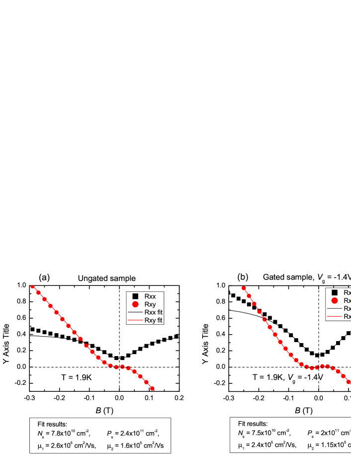
Fig. S2(a) displays and traces of one of the ungated samples. These traces are typical for a system with coexisting electrons and holes. Fitting these traces by using the classical two-component Drude model (see next paragraph) allows to determine the values of 2D electron and hole densities and mobilities. Electron and hole densities of the nm thick HgTe layer are expressed as 2D carrier densities. Values of carrier densities and mobilities extracted from such fits are presented in the boxes underneath the figures in Fig. S2. In comparison with previous results Brune et al. (2011); Olshanetsky et al. (2011) our samples exhibit much smaller carrier densities of typically ( cm-2) and higher mobilities ( cm2/Vs). Both, density decrease and mobility increase indicate that the amount of charged impurities has been significantly reduced by introducing of the CdHgTe buffer layer. The amount of charged impurities in the structure can be estimated from charge neutrality, i.e. cm-2. Taking the thickness of the HgTe layer into account this results in a volume impurity density of cm-3.
I.3 Gated and ungated samples
Whether the Dirac surface states are affected by gate fabrication we studied with some care. In Fig. S2 we compare and of the ungated sample (Fig. S2(a)) and of the gated one (Fig. S2(b)) for an applied gate voltage V. The most important feature here is the overall similarity of the corresponding traces in Fig. S2(a) and (b): by applying an appropriate gate voltage we can bring the gated system into the same state as the ungated one. Direct comparison of electron and hole densities and mobilities, extracted from Drude fits, shows that they are within 20% the same. This is the same level of difference found between samples fabricated the same way. This indicates that gate fabrication does not change the band diagram of the structure qualitatively but introduces charged impurities and/or defects in the system with a density of order of cm-2, varying from sample to sample.
I.4 CdHgTe-capped and open HgTe films
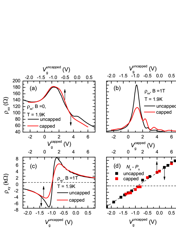
Besides investigating the influence of the gate fabrication on the sample’s charge state we also checked how capping of the HgTe film with a CdHgTe film affects the transport properties (see Fig. S1(a)). In addition we compared different kinds of dielectric layers under the gate. The following results show that the properties of the HgTe film are only weakly dependent on the presence of a cap or different dielectric layers. A comparison between two samples is presented in the Fig. S3. The first one (labeled ”uncapped” in Fig. S3) has an uncapped HgTe film with an insulating SiO2 layer on top and the second one (”capped” in the Fig. 3) is a HgTe film with CdHgTe cap layer and a Al2O3 insulator under the gate. Since dielectric constant and insulator thickness are different for these samples the change of carrier density with gate voltage differs correspondingly: cm-2/V for the Si3N4-covered sample and cm-2/V for the Al2O3-covered one. In order to compare the samples one has to rescale the gate voltage axis with the ratio of the respective specific capacitances. In doing so, the experimental traces in Fig S3(a), (c) and (d) of the two samples follow each other closely. Only some features in and in the presence of a magnetic field and near the charge neutrality point in Fig. S3(b) and (c) differ slightly. In spite of these small differences the general properties of the samples are still the same: all the observed features in transport of the uncapped sample are more or less visible in the measurements of the capped sample and even the estimated gap value between conduction and valence bands is the same – meV. The reproducibility between the two samples made from different wafers is amazing and points to some kind of rigidity of the band structure and Dirac surface states with respect to external disturbances.
II Fitting of magnetoresistance and Hall resistance within the two-component classical Drude model

We used the classical Drude model to extract electron and hole densities and mobilities by fitting and at small magnetic field and for a fixed gate voltage (see Fig. S4). A detailed description of the model can be found in Blatt (1968) and many other textbooks. Here we present only its application to our system. The model is based on the assumption that, in the system studied, groups of noninteracting carriers exist. Each group has charge (electrons or holes), density and mobility . The conductivity of the system is given as the sum over the conductivities of each group: and . After tensor inversion one obtains the corresponding expressions for and .
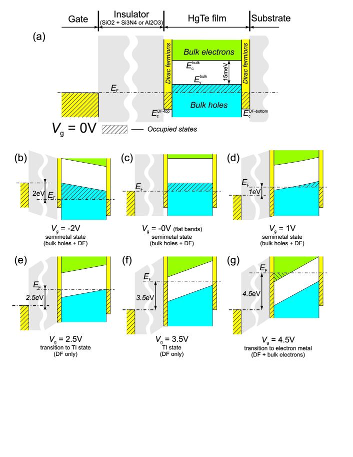
In our system we can distinguish four main groups of carriers: bulk holes in the valence band, bulk electrons in the conduction band and two groups of Dirac fermions (DF) which exist at the two surfaces of the HgTe film. This picture is based on band structure calculations of Brüne et al. (Brune et al. (2011), supplementary). A simplified band scheme which describes the position of the Fermi energy at different gate voltages is presented in Fig. S5. Though the Drude model can, in principle, be used for any number of carrier groups, a reasonable fit is only possible for (trivial case) and . Already for three groups of carriers the expressions become complicated and contain 6 fitting parameters. Then fitting become ambiguous. Due to the gap in the bulk spectrum we have in our case no more than three groups of carriers at (see Fig. S5). To reduce the number of groups further we treat the Dirac electrons of top and bottom surface as one group. This is justified as they have the same charge and since the difference in mobility and carrier density causes only weak corrections to and . When extracting carrier density and mobility of surface electrons we always obtain an average of top and bottom surface. Within this approximation the number of Drude groups is reduced to 2 (bulk holes and Dirac electrons or bulk electrons and Dirac electrons when is located in the valence or conduction band, respectively). With in the bulk gap is even reduced to one as then only Dirac electrons exist.
In case of two of groups of carriers (with index 1 and 2) the system displays a classical parabolic magnetoresistance (MR) with magnitude , where and are the corresponding conductivities of each group at zero magnetic field. The sign between the ’s depends on the carriers’ polarity: in case the carriers have the same polarity (e.g., two groups of electrons) the ”-” sign applies while in the case of different polarity (electrons and holes coexist when Fermi level resides in the valence band) the mobilities add, thus resulting in a strong MR. Hence two groups of Dirac electrons with similar values of their mobility will cause only a small MR effect. This is actually the reason why we can treat top and bottom surface electrons as one species. In contrast, we expect a maximum magnetoresistance when the Fermi level is in the valence band near the the charge neutrality point where and holds. Note that the charge neutrality point is not equal to the Dirac point as the latter is located in the valence band. A significant change of the MR magnitude is expected when the Fermi level moves from the valence band into the gap where only Dirac electrons reside (topological insulator state) and the magnitude of MR drops by up to a factor of 10. The data in Fig. S4(b) show this drastic chance in MR depending on , i.e. . The drastic change of between V and V in Fig. S4(b) also heralds this change in the contributing charge carriers. At V becomes nearly linear indicating that for V only the electrons of the surface states contribute.
The next change of the MR behavior is expected when the Fermi level enters the conduction band. (Fig. S4(c)). There, the presence of low-mobility bulk electrons results in a rise of the MR magnitude (see, e.g., ).
The monotonous decrease of (curvature around ) with increasing is reversed in the small voltage interval between V and V. Because of the relatively small bulk electron density when just enters the conduction band and their small contribution to the overall conductivity, the resulting MR is weaker compared to the situation in the valence band where carriers of different polarity are involved. For further increasing the bulk electrons’ contribution to the conductivity increases but, on the other hand, the mobility increases also resulting in a reduced MR magnitude for V, as displayed in Fig. S4(c).
Thereby the presence of the bulk electrons, starting to appear at V is observed in classical transport. However, the Drude fits are not sensitive enough to disentangle density and mobility of surface and bulk electrons and one could determine the gate voltage corresponding to crossing of Fermi level with the bottom of conductive band but the sensitivity of the Drude fitting technique is not enough to determine exact values of bulk electrons density and mobility.