Surface structure of Bi2Se3(111) determined by low-energy electron diffraction and surface X-ray diffraction
Abstract
The surface structure of the prototypical topological insulator Bi2Se3 is determined by low-energy electron diffraction and surface X-ray diffraction at room temperature. Both approaches show that the crystal is terminated by an intact quintuple layer. Specifically, an alternative termination by a bismuth bilayer is ruled out. Surface relaxations obtained by both techniques are in good agreement with each other and found to be small. This includes the relaxation of the van der Waals gap between the first two quintuple layers.
pacs:
68.35.-p, 61.05.J-, 61.05.C-Bismuth selenide and bismuth telluride have recently attracted considerable attention as prototypical topological insulators. The electronic band structure has a negative band gap at , resulting in an odd number of closed surface state Fermi contours around the centre of the surface Brillouin zone, i.e. in a particularly simple manifestation of topologically protected surface states Noh et al. (2008); Zhang et al. (2009); Xia et al. (2009); Hsieh et al. (2009).
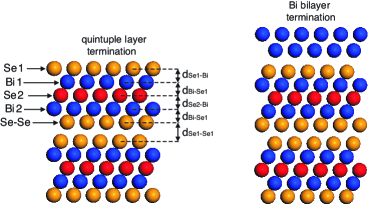
Bi2Se3 has a layered crystal structure, made up from Se-Bi-Se-Bi-Se quintuple layers (QLs), separated by van der Waals gaps (see Figure 1). The (111) surface of the material is the surface parallel to these QLs and can be prepared easily by cleaving the crystal with scotch tape. It therefore appears likely that this cleaving process takes place between two QLs and the surface is thus terminated by an intact QL. However, this termination has recently been questioned by a low energy ion scattering investigation which revealed that a surface obtained by cleaving at room temperature, or left for some time at low temperature, develops a strong enrichment of Bi, consistent with a termination by a bismuth bilayer on top of the last QL of Bi2Se3 He et al. (2013). Such a change of the surface termination (of Bi2Se3 or Bi2Te3) should lead to a drastic modification of the surface electronic structure Hirahara et al. (2011); He et al. (2013); Miao et al. (2013) compared to the single Dirac cone usually observed Xia et al. (2009); Hsieh et al. (2009). Angle-resolved photoemission (ARPES) spectra for Bi2Se3 cleaved at room temperature do not show this more complicated electronic structure Hatch et al. (2011), but it can be created on both Bi2Te3 and Bi2Se3 by depositing a bilayer of bismuth on purpose Hirahara et al. (2011); Miao et al. (2013).
Even for the bulk terminated by a QL, details of the structural relaxations are crucial for the electronic structure. It has been observed early that ARPES spectra from Bi2Se3 change with time after cleave Hsieh et al. (2009). The change manifests itself as a shift of all the bands to higher binding energy and the appearance of new two-dimensional states on the surface Bianchi et al. (2010, 2011). An initial interpretation of this was a structural relaxation of the van der Waals gaps below the surface Noh et al. (2008); Hsieh et al. (2009) and it was shown theoretically that an increased van der Waals gaps could indeed give rise to two-dimensional electronic states that are similar to those observed by ARPES Menshchikova et al. (2011); Vergniory et al. (2012). In related layered systems with van der Waals gaps, such a surface relaxation can in fact reproduce observed splittings of ARPES band dispersions Hoesch et al. (2009). Intercalating of atoms into Bi2Se3 to increase the van der Waals gap spacing on purpose, however, did not lead to changes in the electronic structure Bianchi et al. (2012), and an alternative interpretation of the phenomenon is the formation of two-dimensional electron gases near the surface caused by an adsorbate-induced band bending Bianchi et al. (2010, 2011); Bahramy et al. (2012); King et al. (2011).
A detailed structural determination of the Bi2Se3(111) surface cleaved at room temperature is therefore called for and presented here. We use two complementary and powerful structural techniques, low-energy electron diffraction (LEED) and surface X-ray diffraction (SXRD).
The Bi2Se3 crystals were grown by standard methods described elsewhere Bianchi et al. (2010). The bulk structure was determined by X-ray diffraction at room temperature. To this end, a fine powder was filed from the crystal rod and diffraction experiments were performed on a STOE powder diffractometer using Cu Kα1 radiation in transmission geometry. The bulk structure parameters were analysed by Rietveld refinement and found to be in good agreement with the literature Nakajima (1963). These structural parameters were used as starting and reference points for the surface structure determination. LEED and SXRD experiments were performed in ultra-high vacuum (UHV) chambers with a base pressure of Torr. The samples were cleaved at room temperature in a loadlock with a somewhat inferior pressure. X-ray photoemission spectroscopy performed in the LEED chamber did not show any detectable contaminations. SXRD data were taken at beamline I07 of the Diamond Light Source, using 20 keV X-rays and a UHV chamber mounted on a large ’2+3’ diffractometer Vlieg (1998). Scattered X-rays were collected using a two-dimensional detector (Pilatus) enabling fast data acquisition. The specular reflectivity (00 rod) was collected using a conventional scan, whilst all non-specular data was recorded using a fixed X-ray incidence angle of 1∘. Note that data were acquired over a time span in the order of hours, whereas Ref. He et al. (2013) reports an increased Bi concentration near the surface, interpreted as a bilayer formation, immediately after cleaving the sample at room temperature.
Full dynamic LEED I(V) model calculations were performed using a modified version of the Symmetrised Automated Tensor LEED (SATLEED) computer package Barbieri and van Hove ; Van Hove et al. (1986). The potential and the electron scattering phase-shifts for the Bi2Se3 (111) surface were calculated using the optimised muffin-tin potential method Rundgren (2003), an approach recently used to successfully determine complex metal oxide surfaces Nascimento et al. (2007); Pentcheva et al. (2008); Nascimento et al. (2009). Specific phase-shift sets were calculated for selenium and for bismuth atoms, depending on their surface and bulk positions. The I(V) model calculations converged when using 12 phase shifts (); and 13 phase shifts were used in the final calculations. Convergence for a lower number of phase shifts than in e.g. Ref. Fukui et al. (2012) is probably caused by two factors: one is the different method of phase shift calculations and the other is the lower maximum electron energy in the experiment, which was found sufficient due to the higher temperature. Debye temperatures were obtained from Ref. Shoemake et al. (1969). The real and imaginary parts of the optical potential were set to eV and -5.0 eV, respectively.
SXRD crystal truncation rod intensities were extracted by numerically integrating the background-subtracted spot in a well defined region of interest on the detector image. The structure factors were calculated by applying correction factors to account for the polarisation of the X-ray beam, the rod interception, and the area of the sample contributing to the scattered intensity, and then taking the square root of the corrected intensity Schlepütz et al. (2011). Subsequent analysis of the data was undertaken using the ANAROD code Vlieg (2000).
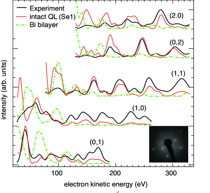
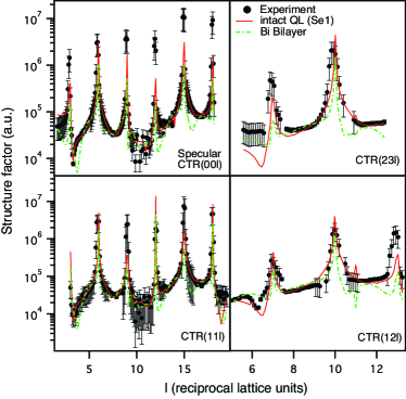
The structure determination was performed by a quantitative comparison between the experimental and theoretical I(V) curves and crystal truncation rod intensities. The agreement between experimental data and model calculations was quantified using the Pendry reliability factor () Pendry (1980) and by for LEED and SXRD, respectively. In the first step of the structure analysis, five bulk truncated trial models were tried: the different possible possible bulk terminations (Se1, Bi1, Se2, Bi2, and Se-Se, see Fig. 1) as well a bismuth bilayer atop of the truncated bulk crystal. The resulting agreement is shown Table 1. After that, an optimisation procedure was used to adjust the structural parameters as well as the inner potential (for LEED) to find the optimum structure, namely the one that leads to the lowest or . For the LEED analysis of the Se1 structure, the surface Debye temperatures of the first four layers were refined, too, but this gave only rise to a very small change of . The final values of and for all structural models are also listed in Table 1. Regarding the Bi bilayer atop model He et al. (2013), all the nine stacking possibilities were tested and the structural parameters of the bilayer were refined. The best values of and are given in Table 1. The final comparison between measured and calculated diffraction data are shown in Figures 2 and 3, both for the best fit obtained with the intact QL (Se1) termination as well as for the best agreement that can be reached with an optimised Bi bilayer termination.
| LEED | SXRD | |||
|---|---|---|---|---|
| Model | Bulk | Optimised | Bulk | Optimised |
| Se1 | 0.74 | 0.25 | 3.15 | 2.44 |
| Bi1 | 0.83 | 0.61 | 9.50 | 4.68 |
| Se2 | 0.91 | 0.70 | 30.32 | 10.20 |
| Bi2 | 0.80 | 0.65 | 30.31 | 7.02 |
| Se-Se | 0.98 | 0.80 | 9.46 | 7.05 |
| Bi atop He et al. (2013) | 1.00 | 0.84 | 11.88 | 6.31 |
For both LEED and SXRD, the termination with an intact QL, i.e. the Se1 model, gives the best agreement between experimental and simulated diffraction data. The detailed structural relaxations for this termination are given in Table 2. The agreement between the two structural techniques is excellent, apart from the third interlayer distance where LEED finds a slightly larger expansion than SXRD, and the fourth interlayer distance where LEED points towards a small contraction of the interlayer spacing whereas SXRD shows an expansion. Both techniques are consistent in finding a small contraction in the first interlayer spacing and a small expansion of the van der Waals gap distance .
| Interlayer Distances | Bulk Value | LEED | SXRD |
|---|---|---|---|
| 1.62 | 1.56 0.03 | 1.51 0.05 | |
| 1.95 | 1.96 0.03 | 1.94 0.06 | |
| 1.95 | 2.01 0.04 | 1.91 0.05 | |
| 1.62 | 1.53 0.05 | 1.72 0.04 | |
| 2.42 | 2.51 0.08 | 2.50 0.06 |
From the results of this structural determination, we can draw the following conclusions: Both techniques unambiguously show that, at room temperature, the Bi2Se3(111) surface is terminated with an intact QL rather than covered by a Bi bilayer. An intact QL termination also suggest that this termination prevails at lower temperature, since less thermal activation energy is available for a major structural rearrangement. The observed termination is at variance with the recent low-energy ion scattering result report in Ref. He et al. (2013) but consistent with other experimental evidence. Notably, the surface electronic structure for a Bi bilayer on Bi2Se3(111) is quite different Miao et al. (2013) from the simple single Dirac cone observed for the surface terminated by a van der Waals gap. While only low-temperature ARPES data for an on-purpose prepared bilayer of Bi on Bi2Se3(111) are available, it is unlikely that a room temperature measurement such as in Ref. Hatch et al. (2011) would miss the electronic structure change and the additional bands caused by the bilayer. Finally, it is interesting to note that a recent room temperature SXRD structural determination of thin Bi2Te3 films on Si has a also shown the films to have a intact QL termination towards vacuum Liu et al. (2013).
The details of the surface relaxations are also interesting. The contraction of the first interlayer spacing is of the order of 5% and such a large contraction is unusual for a closed packed surfaces. On closed-packed simple metal surfaces, small expansions of the first interlayer spacing are more frequently found than contractions Hofmann et al. (1996). On Bi2Te3(111), a small contraction of 1 % was reported Fukui et al. (2012). More importantly, neither LEED nor SXRD find a significant expansion on the first van der Waals gap spacing. Both point towards a small expansion in the order of 4 %, far smaller than the expansions of 20 - 40 % required to explain the observed two-dimensional electronic states in the conduction band as caused by an interlayer expansion Menshchikova et al. (2011); Vergniory et al. (2012). This can be taken as additional evidence that band bending, an not surface relaxation, is the cause for the appearance of new two-dimensional electronic states near the surface of Bi2Se3 Bianchi et al. (2010, 2011); Bahramy et al. (2012); King et al. (2011).
In summary, LEED and the SXRD reveal that the room temperature structure of Bi2Se3(111) is that of a surface terminated by an intact QL, i. e. as expected for a surface cleaved in a van der Waals gap. Both techniques agree on a small expansion of the first van der Waals gap below the surface but the size of the expansion is far smaller than what would be required to bring about a dramatic change of the surface electronic structure.
Acknowledgements.
We gratefully acknowledge financial support by the VILLUM foundation, the Danish National Research Foundation, the Carslberg foundation, CNPq, CAPES, FAPEMIG, and the Laboratório Nacional de Luz Síncrotron (LNLS), as well as travel support from the Diamond Light Source Ltd. under proposal SI7522.References
- Noh et al. (2008) H.-J. Noh, H. Koh, S.-J. Oh, J.-H. Park, H.-D. Kim, J. D. Rameau, T. Valla, T. E. Kidd, P. D. Johnson, Y. Hu, et al., Europhysics Letters 81, 57006 (2008).
- Zhang et al. (2009) H. Zhang, C.-X. Liu, X.-L. Qi, X. Dai, Z. Fang, and S.-C. Zhang, Nature Physics 5, 438 (2009).
- Xia et al. (2009) Y. Xia, D. Qian, D. Hsieh, L. Wray, A. Pal, H. Lin, A. Bansil, D. Grauer, Y. S. Hor, R. J. Cava, et al., Nature Physics 5, 398 (2009).
- Hsieh et al. (2009) D. Hsieh, Y. Xia, D. Qian, L. Wray, J. H. Dil, F. Meier, J. Osterwalder, L. Patthey, J. G. Checkelsky, N. P. Ong, et al., Nature 460, 1101 (2009).
- He et al. (2013) X. He, W. Zhou, Z. Y. Wang, Y. N. Zhang, J. Shi, R. Q. Wu, and J. A. Yarmoff, Phys. Rev. Lett. 110, 156101 (2013).
- Hirahara et al. (2011) T. Hirahara, G. Bihlmayer, Y. Sakamoto, M. Yamada, H. Miyazaki, S.-i. Kimura, S. Blügel, and S. Hasegawa, Phys. Rev. Lett. 107, 166801 (2011).
- Miao et al. (2013) L. Miao, Z. F. Wang, W. Ming, M.-Y. Yao, M. Wang, F. Yang, Y. R. Song, F. Zhu, A. V. Fedorov, Z. Sun, et al., Proceedings of the National Academy of Sciences 110, 2758 (2013).
- Hatch et al. (2011) R. C. Hatch, M. Bianchi, D. Guan, S. Bao, J. Mi, B. B. Iversen, L. Nilsson, L. Hornekær, and Ph. Hofmann, Phys. Rev. B 83, 241303 (2011).
- Bianchi et al. (2010) M. Bianchi, D. Guan, S. Bao, J. Mi, B. B. Iversen, P. D. C. King, and Ph. Hofmann, Nature Communications 1, 128 (2010).
- Bianchi et al. (2011) M. Bianchi, R. C. Hatch, J. Mi, B. B. Iversen, and Ph. Hofmann, Phys. Rev. Lett. 107, 086802 (2011).
- Menshchikova et al. (2011) T. V. Menshchikova, S. V. Eremeev, and E. V. Chulkov, JETP Letters 94, 106 (2011).
- Vergniory et al. (2012) M. Vergniory, T. Menshchikova, S. Eremeev, and E. Chulkov, JETP Letters 95, 213 (2012).
- Hoesch et al. (2009) M. Hoesch, X. Cui, K. Shimada, C. Battaglia, S.-i. Fujimori, and H. Berger, Phys. Rev. B 80, 075423 (2009).
- Bianchi et al. (2012) M. Bianchi, R. C. Hatch, Z. Li, Ph. Hofmann, F. Song, J. Mi, B. B. Iversen, Z. M. Abd El-Fattah, P. Löptien, L. Zhou, et al., ACS Nano 6, 7009 (2012).
- Bahramy et al. (2012) M. S. Bahramy, P. D. C. King, A. de la Torre, J. Chang, M. Shi, L. Patthey, G. Balakrishnan, Ph. Hofmann, R. Arita, N. Nagaosa, et al., Nat Commun 3, 1159 (2012).
- King et al. (2011) P. D. C. King, R. C. Hatch, M. Bianchi, R. Ovsyannikov, C. Lupulescu, G. Landolt, B. Slomski, J. H. Dil, D. Guan, J. L. Mi, et al., Phys. Rev. Lett. 107, 096802 (2011).
- Nakajima (1963) S. Nakajima, J. Phys. Chem. Solids 24, 479 (1963).
- Vlieg (1998) E. Vlieg, J. Appl. Cryst. 31, 198 (1998).
- (19) A. Barbieri and M. A. van Hove, software available at http://www.icts.hkbu.edu.hk/vanhove.
- Van Hove et al. (1986) M. A. Van Hove, W. H. Weinberg, and C. M. Chan, Low energy electron diffraction (Springer-Verlag, Berlin, 1986).
- Rundgren (2003) J. Rundgren, Phys. Rev. B 68, 125405 (2003).
- Nascimento et al. (2007) V. B. Nascimento, R. G. Moore, J. Rundgren, J. Zhang, L. Cai, R. Jin, D. G. Mandrus, and E. W. Plummer, Phys. Rev. B 75, 035408 (2007).
- Pentcheva et al. (2008) R. Pentcheva, W. Moritz, J. Rundgren, S. Frank, D. Schrupp, and M. Scheffler, Surf. Sci. 602, 1299 (2008).
- Nascimento et al. (2009) V. B. Nascimento, J. W. Freeland, R. Saniz, R. G. Moore, D. Mazur, H. Liu, M. H. Pan, J. Rundgren, K. E. Gray, R. A. Rosenberg, et al., Phys. Rev. Lett. 103, 227201 (2009).
- Fukui et al. (2012) N. Fukui, T. Hirahara, T. Shirasawa, T. Takahashi, K. Kobayashi, and S. Hasegawa, Phys. Rev. B 85, 115426 (2012).
- Shoemake et al. (1969) G. E. Shoemake, J. A. Rayne, and R. W. Ure, Phys. Rev. 185, 1046 (1969).
- Schlepütz et al. (2011) C. M. Schlepütz, S. O. Mariager, S. A. Pauli, R. Feidenhans’l, and P. R. Willmott, Journal of Applied Crystallography 44, 73 (2011).
- Vlieg (2000) E. Vlieg, J. Appl. Cryst. 33, 401 (2000).
- Pendry (1980) J. B. Pendry, Journal of Physics C: Solid State Physics 13, 937 (1980).
- Liu et al. (2013) Y. Liu, H.-H. Wang, G. Bian, Z. Zhang, S. S. Lee, P. A. Fenter, J. Z. Tischler, H. Hong, and T.-C. Chiang, Phys. Rev. Lett. 110, 226103 (2013).
- Hofmann et al. (1996) Ph. Hofmann, K. Pohl, R. Stumpf, and E. W. Plummer, Physical Review B 53, 13715 (1996).