Soft-boundary graphene nanoribbon formed by a graphene sheet above a perturbed ground plane: conductivity profile and SPP modal current distribution
Abstract
An infinite sheet of graphene lying above a perturbed ground plane is studied. The perturbation is a two dimensional ridge, and a bias voltage is applied between the graphene and the ground plane, resulting in a graphene nanoribbon-like structure with a soft-boundary (SB) The spatial distribution of the graphene conductivity forming the soft-boundary is studied as a function of the ridge parameters and the bias voltage. The current distribution of the fundamental TM surface plasmon polariton (SPP) is considered. The effect of the ridge parameters and shape of the soft boundary on the current distributions are investigated, and the conditions are studied under which the mode remains confined to the vicinity of the ridge region.
1 Introduction
Graphene is a two-dimensional material having unique electronic, mechanical, and optical properties [1, 2, 3, 4, 5, 6]. A variety of applications have been considered, including optical sensors [7], transparent electrodes, nanoelectromechanical applications (NEMs) [8], and optoelectronic applications [9, 10, 11, 12]. Graphene’s interesting properties are partly because of its conical conduction and valance bands joined by two points at the Fermi level [13]. Graphene, doped with excess carriers, can also guide surface plasmon oscillations at terahertz frequencies, similar to those in noble metals at infrared frequencies [14, 15]. In this regard, graphene is considered a better plasmonic material than nobel metals with greater confinement of the electromagnetic energy and lower loss. Compared to noble-metal plasmons, graphene modes have two major advantages, 1) they are long-lived excitations because of the low loss of graphene, and 2) their frequency can are controlled by electrostatic doping. The tunability of transverse magnetic (TM) surface plasmons is due to the ability to vary the carrier density, which can be easily achieved by gate biasing or chemical doping. Graphene can also support transverse electric (TE) surface plasmons which are loosely confined to its surface; we do not consider them further in this paper. Electron energy-loss spectroscopy (EELS) was first used to prove the existence of the plasmonic effect in graphene experimentally [16, 17]. Later, surface plasmons were excited with optical means and the interaction of optical phenomena with graphene plasmons was studied experimentally [18, 19]. Considering only TM surface plasmons, an infinite suspended sheet of graphene supports one surface mode. However, a graphene strip supports an infinite number of 2D-bulk modes and two almost degenerate symmetrical and anti-symmetrical edge modes. Therefor, graphene strips are of obvious interest for waveguiding and related applications due to the variety of possible modes that may propagate. Also, plasmons in graphene with a magnetic field present have been studied [20, 21] and shown to have interesting properties. For example, a magnetically biased graphene strip supports edge and bulk magnetoplasmons with nonreciprocal properties. Electrically, graphene can be modeled by a surface conductivity which is considered in several works [22, 23, 24, 25, 26, 27, 28, 29, 30]. Here we use the local conductivity resulting from the Kubo formula [31]
| (1) |
where is the charge of an electron, is the reduced Plank’s constant, is the Fermi-Dirac distribution, is the Boltzmann’s constant, is the inhomogeneous chemical potential created by the bias, and 1/s is the phenomenological scattering rate.

The first term in (1) is due to intraband contributions and the second term is due to interband contributions. The sign of is negative and positive for the intraband and interband contributions, respectively. Therefore, depending on the parameters in (1), such as frequency and temperature, one of the two contributions dominates and determines the sign of .
It can be shown that TM surface waves can propagate only if [24, 28]. This phenomena is exploited in [32], where it is suggested that a graphene sheet and an inhomogeneous biasing scheme, such as that resulting from a ground plane ridge (Fig. 1), can be used to electronically form a conductivity profile capable of confining SPP propagation. That is, in [32] the ridge is assumed to achieve a piece-wise constant conductivity profile with in the desired channel region and outside of the channel, , forming, essentially, a hard-boundary (HB) graphene nanoribbon (GNR). In this paper, we investigate this structure (Fig. 1) without the piece-wise constant conductivity assumption - the biased ridge/ground plane results in an electrostatic (bias) charge distribution determined from Laplace’s equation, which, in turn, results in the inhomogeneous chemical potential such that . This geometry allows the ability to tune to be negative in a limited area (in the vicinity of the ridge), forming a channel for SPP guiding, albeit forming a soft boundary. In particular, it is impossible to form the hard boundary case using the ridged ground plane, but one can approximate the HB case with a sufficiently-sharp soft boundary, as shown below.
The time convention is and the temperature in (1) is set to be K, consistent with [32], since at lower temperature the interband contribution can dominate the intraband contribution down to lower frequencies then at room temperature. For example, at and the intraband and interband contributions at K are and while at K they are and .
In the following, properties of the resulting channel are studied as a function of the parameters shown in figure 1. Then, the current distribution of the fundamental mode of the geometry is considered and the conditions are explored under which the mode will remain confined to the vicinity of the step region. One interesting result is that currents can still be concentrated to the vicinity of the ridge even when is negative everywhere. This requires some special conditions which are discussed toward the end of this work.
2 Methodology and formulations
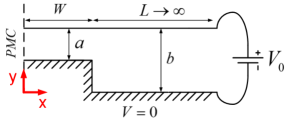
Figure 2 shows the x-y view of the geometry in figure 1. A perfect magnetic conductor sheet (PMC) is placed at since the geometry is symmetrical with respect to . By solving Laplace’s equation and applying the appropriate boundary conditions, it is easy to show that the bias voltage distribution between the graphene and ground plane is
| (2) |
where
| (3) |
In obtaining (2), a zeroth order approximation has been used to assume an x- independent potential in the region above the step (). Otherwise, the problem needs to be solved numerically (e.g., by expanding the potentials as series for both and regions). The zeroth-order solution is a good approximation for and/or in Fig. 1.
Therefore, the electrostatic surface charge density on the graphene sheet is
| (4) |
which can be used to find the chemical potential on the graphene sheet as
| (5) |
where m/s is the Fermi velocity. Eq. (1) then gives the conductivity distribution on the graphene sheet.
In order to find the dynamic modal current distributions on the graphene (eigencurrents of the structure), Ohm’s law can be used in the one dimensional Fourier transform domain as
| (6) |
where the Fourier transform pair is defined as
| (7) |
| (8) |
Green’s theorem relates the current and the electric field as
| (9) |
| (11) |
where is the zero’s order modified Bessel function of the first kind. Since we are considering modes tightly bound to the graphene surface, once the ridged ground plane is used to obtain the electrostatic bias charge density we assume that the ground plane does not interact with the tightly-confined modal fields, which we verified to be true.
In summary, we assume the graphene sheet forms a conductive surface, we find the electrostatic potential distribution via Laplace’s equation, leading to the electrostatic charge distribution and the resulting chemical potential, resulting in the conductivity . Equations (6) and (9) form an integral equation whose null space gives the modes of the structure (i.e. different and their associated currents).
The pulse function collocation method is used to solve the integral equation, with point matching at the center of the pulses. The conductivity distribution based on the electrostatic charge distribution in (6) is assumed to be only slightly perturbed by the modal fields, i.e., where is the static charge density (4) and is the dynamic modal current density (6). To see that this inequality is satisfied, assume a typical frequency of THz and strip width . If the modal current is as large as mA, then the left side of the inequality is C/. Using (4) with typical values and leads to mC/ (consistent with typical doping densities of ), and the inequality is strongly satisified.
3 Results and discussions
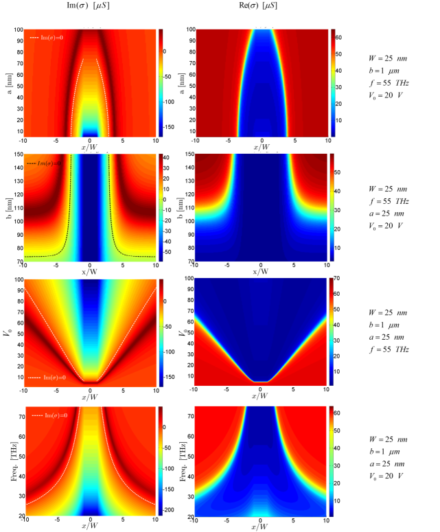
Figure 3 shows the conductivity distribution for the structure of figure 1 as a function of the ridge parameters ( and ), bias voltage, and frequency. The dashed lines in the plots for specify lines where , and so the distance between the dashed lines specifies the effective width of the channel created above the ridge with negative . As can be seen in figure 3, the width of the channel increases by increasing the bias voltage, by decreasing or , or by decreasing frequency (assuming that the other parameters are fixed in each case). The width of the channel is also more sensitive to the applied bias voltage then the other parameters. The parameter along with the bias voltage determines the value of the conductivity in the region. The parameter along with the bias voltage determines the value of the conductivity far away from the ridge However, the softness or the sharpness of the boundary is a function of all the parameters somewhat equally.
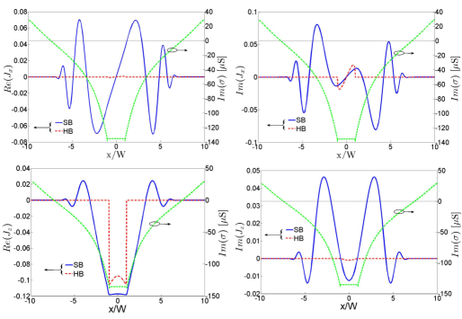
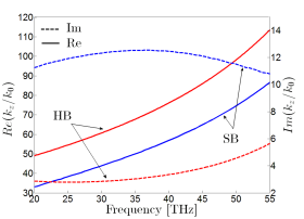
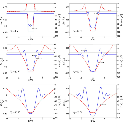
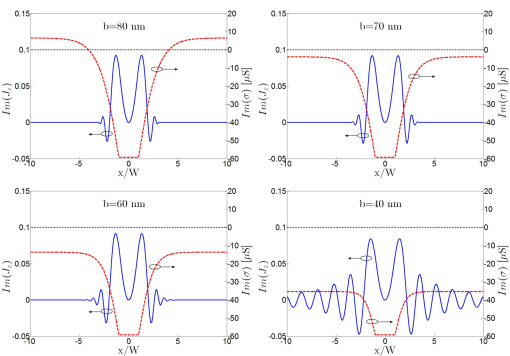
Figure 4 shows the current distribution associated with the fundamental SPP mode of figure 1. The conductivity and the current marked as SB in figure 4 correspond to the geometry in figure 1 for , , and . The current which is noted as the hard boundary current corresponds to a graphene nanoribbon having width of and the same conductivity as the SB case for , and with for . The dispersion curves associated with these currents are shown in figure 5. The currents in figure 4 are normalized so that the 2-norm of the eigencurrent vector (consisting of transverse and longitudinal components) is unity, Nonetheless, only the relative current component values are important for our purposes.
As figure 4 suggests, the current distribution for is similar for both soft and hard boundary cases (although and are much larger in the SB case) and they both vanish as becomes positive. However, the SB current has some oscillations near the two boundaries. These oscillations resemble the field oscillations in the cladding of an optical fiber with graded index cladding [34]. One of the consequences of this current spreading is that the mode becomes more lossy since parts of the current flows in the region with lower conductivity (soft boundaries). As an example, the propagation constant for the SB and HB cases of figure 4 are and , respectively.
Figure 6 shows the effect of the boundary softness on the current distribution () of the fundamental mode, where , , and takes different values. The parameter is set to be so that the conductivity values remains the same for . As figure 6 shows, the boundary becomes softer as increases and the current oscillations increases (both in magnitude and number).
In figures 4 and 6 the currents vanish as becomes positive, which raises the question: is it necessary for to be positive away from the ridge to have a confined mode? To address this question, figure 7 shows and conductivity distributions for different values of ; the other parameters are , , and As figure 7 shows, changes sign for , but it remains negative everywhere for and 40 . The currents remain confined to the vicinity of the ridge region even for values of where remains negative everywhere. However, as decreases the current spreads out further and the mode becomes less confined. As a result, the important factor to achieve good lateral mode confinement is that the ratio of (or the difference between) above and away from the ridge should be large.
4 Conclusion
The conductivity and the current distributions were studied for an infinite graphene sheet over a ridge-perturbed ground plane. It was shown analytically that a channel with soft boundaries will be formed above the ridge to guide SPPs provided that the parameters are adjusted properly. It was also shown that the width of the channel is more sensitive to the bias voltage than the geometric ridge parameters. It was observed that the SPP can be kept confined to the vicinity of the ridge even if the formed channel does not have a finite width (i.e., that is negative everywhere) provided that the channel boundaries have sharp enough slopes. Since the width of the formed channel can be controlled by both frequency and the bias voltage, the spatial location of the current concentration (and its associated field) for a surface mode can be controlled. This can be useful in switching or frequency demultiplexing applications.
References
References
- [1] K. S. Novoselov, A. K. Geim, S. V Morozov, Y. Jiang, D.and Zhang, S. V. Dubonos, I. V. Grigorieva, and A. A. Firsov. Electric field effect in atomically thin carbon films. Science, 306:666–669, 2004.
- [2] Y. Zhang, Y. W. Tan, H. L. Stormer, and P. Kim. Experimental observation of the quantum hall effect and berry’s phase in graphene. Nature, 438:201–204, 2005.
- [3] C. Berger, Z. Song, X. Li, X. Wu, N. Brown, C. Naud, D. Mayou, T. Li, J. Hass, and A. N. Marchenkov. Electronic confinement and coherence in patterned epitaxial graphene. Science, 312:1191–1196, 2006.
- [4] A. K. Geim and K. S. Novoselov. The rise of graphene. Nat. Mater., 6:183–191, 2007.
- [5] R. R. Nair, P. Blake, A. N. Grigorenko, K. S. Novoselov, T. J. Booth, T. Stauber, N. M. R. Peres, and A. K. Geim. Fine structure constant defines visual transparency of graphene. Science, 320:1308, 2008.
- [6] F. Bonaccorso, Z. Sun, T. Hasan, and A. C. Ferrari. Graphene photonics and optoelectronics. Nat. Photon, 4:611–622, 2010.
- [7] F. Schedin, E. Lidorikis, A. Lombardo, V. G. Kravets, A. K. Geim, A. N. Grigorenko, K. S. Novoselov, and A. C. Ferrari. Surface-enhanced raman spectroscopy of graphene. ACS Nano, 4:5617–5626, 2010.
- [8] A. K. Geim. Graphene: Status and prospects. Science, 324:1530–1534, 2009.
- [9] K. F. Mak, M. Y. Sfeir, Y. Wu, C. H. Lui, J. A Misewich, and T. F. Heinz. Measurement of the optical conductivity of graphene. Phys. Rev. Lett., 101:196405, 2008.
- [10] T. Mueller, F. Xia, M. Freitag, J. Tsang, and P. Avouris. Role of contacts in graphene transistors: A scanning photocurrent study. Phys. Rev. B, 79:245430, 2009.
- [11] F. N. Xia, T. Mueller, Y. M. Lin, A. Valdes-Garcia, and P. Avouris. Ultrafast graphene photodetector. Nat. Nanotechnol., 4:839–843, 2009.
- [12] E. J. H. Lee, K. Balasubramanian, R. T. Weitz, M. Burghard, and K. Kern. Contact and edge effects in graphene devices. Nat. Nanotechnol., 3:486–490, 2008.
- [13] A. H. Castro Neto, F. Guinea, N. M. R. Peres, K. S. Novoselov, and A. K. Geim. The electronic properties of graphene. Rev. Mod. Phys., 81:109–162, 2009.
- [14] Johan Christensen, Alejandro Manjavacas, Sukosin Thongrattanasiri, Frank H. L. Koppens, and F. Javier Garcia de Abajo. Graphene plasmon waveguiding and hybridization in individual and paired nanoribbons. ACS Nano, 6:431–440, 2011.
- [15] G. W. Hanson, Ebrahim Forati, Whitney Linz, and A.B. Yakovlev. Excitation of thz surface plasmons on graphene surfaces by an elementary dipole and quantum emitter: Strong electrodynamic effect of dielectric support. Phys. Rev. B, 86:235440 (1–9), 2012.
- [16] Y. Liu, R. F. Willis, K. V. Emtsev, and T. Seyller. Plasmon dispersion and damping in electrically isolated two-dimensional charge sheets. Phys. Rev. B, 78:201403, 2008.
- [17] R. J. Koch, T. Seyller, and J. A. Schaefer. Strong phonon-plasmon coupled modes in the graphene/silicon carbide heterosystem. Phys. Rev. B, 82:201413, 2010.
- [18] L. Ju, B. Geng, J. Horng, C. Girit, M. Martin, Z. Hao, H. A. Bechtel, X. Liang, A. Zettl, Y. R. Shen, and F. Wang. Graphene plasmonics for tunable terahertz metamaterials. Nature Nanotechnol., 6:630 634, 2011.
- [19] H. Yan, X. Li, B. Chandra, G. Tulevski, Y. Wu, M. Freitag, W. Zhu, P. Avouris, and F. Xia. Tunable infrared plasmonic devices using graphene/insulator stacks. Nature Nanotechnol., 7:330 334, 2012.
- [20] R. Roldan, J.-N. Fuchs, and M. O. Goerbig. Collective modes of doped graphene and a standard two-dimensional electron gas in a strong magnetic field: Linear magnetoplasmons versus magnetoexcitons. Phys. Rev. B, 80:085408, 2009.
- [21] A. Ferreira, N. M. R. Peres, and A. H. Castro Neto. Confined magneto-optical waves in graphene. Phys. Rev. B, 85:205426, 2012.
- [22] L. A. Falkovsky and A. A. Varlamov. Space-time dispersion of graphene conductivity. Eur. Phys. J. B, 56:281–284, 2007.
- [23] L. A. Falkovsky and S. S. Pershoguba. Optical far-infrared properties of a graphene monolayer and multilayer. Phys. Rev. B, 76:153410, 2007.
- [24] S. A. Mikhailov and K. Ziegler. New electromagnetic mode in graphene. Phys. Rev. Lett., 99:016803, 2007.
- [25] V. P. Gusynin and S. G. Sharapov. Transport of dirac quasiparticles in graphene: Hall and optical conductivities. Phys. Rev. B, 73:245411, 2006.
- [26] V. P. Gusynin, S. G. Sharapov, and J. P. Carbotte. Unusual microwave response of dirac quasiparticles in graphene. Phys. Rev. Lett., 96:256802, 2006.
- [27] N. M. R. Peres, AH Castro Neto, and F. Guinea. Conductance quantization in mesoscopic graphene. Phys. Rev. B, 73:195411, 2006.
- [28] G. W. Hanson. Dyadic greens functions and guided surface waves for a surface conductivity model of graphene. J. Appl. Phys., 103:064302, 2008.
- [29] G. W. Hanson. Dyadic green’s functions for an anisotropic, non-local model of biased graphene. IEEE Trans. Antennas Propagat., 56:747–757, 2008.
- [30] K. Ziegler. Minimal conductivity of graphene: Nonuniversal values from the kubo formula. Phys. Rev. B, 75:233407, 2007.
- [31] V. P. Gusynin, S. G. Sharapov, and J. P. Carbotte. Magneto-optical conductivity in graphene. J. Phys.: Condens. Matter, 19.2:026222, 2007.
- [32] Ashkan Vakil and Nader Engheta. Transformation optics using graphene. Science, 332.6035:1291–1294, 2011.
- [33] W.C. Chew. Waves and Fields in Inhomogeneous Media. IEEE Press, 1995.
- [34] M. Kong and B. Shi. Field solution and characteristics of cladding modes of optical fibers. Fiber and integrated optics, 25:305–321, 2006.