Optical properties of single ZnTe nanowires grown at low temperature
Abstract
Optically active gold-catalyzed ZnTe nanowires have been grown by molecular beam epitaxy, on a ZnTe(111) buffer layer, at low temperature () under Te rich conditions, and at ultra-low density (from 1 to 5 nanowires per ). The crystalline structure is zinc blende as identified by transmission electron microscopy. All nanowires are tapered and the majority of them are oriented. Low temperature micro-photoluminescence and cathodoluminescence experiments have been performed on single nanowires. We observe a narrow emission line with a blue-shift of 2 or 3 meV with respect to the exciton energy in bulk ZnTe. This shift is attributed to the strain induced by a 5 nm-thick oxide layer covering the nanowires, and this assumption is supported by a quantitative estimation of the strain in the nanowires.
pacs:
78.55.Et, 78.60.Hk, 81.15.Hi, 81.05.DzThere is currently a wide-spread interest for semiconductor nanowires (NWs), driven by their potential to constitute suitable building blocks for future nanoelectronic and nanophotonic devices. Duan01 During the past decade, selenide and telluride II-VI NWs have been extensively investigated for various applications such as nano-pillar solar cells,Fan09 photodetectors Meng09 or single photon sources.Boun12 Among II-VI’s, ZnTe based NWs are particularly promising as offering a large range of potentialities. They can be grown by molecular beam epitaxy (MBE) using gold particles as catalyst. They can be efficiently doped electrically. Liu13 They can also be doped with magnetic impurities, Rada05 ; Wojn12 while the large difference between the temperatures suitable for the growth of GaAs NWs and for the incorporation of Mn as substitutional impurities makes the growth of (Ga,Mn)As NWs challenging.Bouravleuv13 As (Zn,Mn)Te can be doped strongly p-type so that ferromagnetism appears and transport studies are feasible in 2D,Ferrand01 ZnTe-based NWs are attractive for a basic study of spintronics mechanisms in 1D. In addition, CdTe quantum dots can be incorporated and used as a single photon source Wojn11 or as a very sensitive optical probe of the spin properties. Beso04
A good control and the optimization of the growth conditions are prerequisites to improve the electronic and optical properties of the NWs. We present the MBE growth and the structural analysis of ultra-low density ZnTe NWs and we show that their high crystalline quality allows us to observe micro-photoluminescence (PL) and cathodoluminescence (CL) emission from single NWs.
ZnTe NWs were grown by MBE, using gold particles as a catalyst. A thin layer of gold was deposited on a 500 nm-thick ZnTe(111) buffer layer previously grown on a GaAs(111)B substrate. Gold droplets were formed at and the NWs were grown at the same temperature. As we observed that Te-rich conditions result in a larger diffusion length on the (111) ZnTe surface,Rueda13 the present NWs were grown with a Zn:Te flux ratio 1:2.3, for 30 or 60 min. More details are given in Ref. Rueda13, .
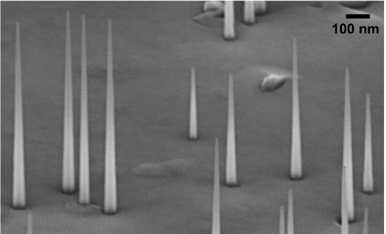
Typical ZnTe NWs have been imaged by scanning electron microscopy (SEM), see Fig. 1. This sample presents an ultra-low-density of NWs, down to 2 NWs per . These NWs grown under Te-rich conditions are tapered, with a thick base (50-70 nm) and a thin tip (15 nm roughly equal to the gold particle diameter) . This cone shape is due to lateral growth induced by the low growth temperature.Rueda13 The NW height distribution is large, from to for a 30 min growth time.
The majority (about two thirds) of the NWs are oriented , and most of the remaining NWs oriented . Transmission Electron Microscopy (TEM) was performed on a Philips CM300 microscope equipped with a CCD camera and operated at 300 kV. Images reveal a zinc-blende crystal structure, see Fig. 2. Some NWs do not present any defect, but many of them show twins, as frequently observed in zinc-blende NWs. We systematically observe an amorphous layer (5 nm thick) all around the NW, which we attribute to oxidation after growth (see Fig. 2b). ZnTe(111) surfaces tend to be rapidly oxidized either by forming \ceTe O_2 or/and ZnO Ebina1978_ZnTeOxide . In the case of ZnTe NWs, the formation of a partially crystallized ZnO shell has been reported,Kirmse08 although the presence of Te-oxide in the outermost part was also suggested by electron energy loss spectroscopy analysis. In our samples, energy dispersive x-ray analysis (EDX) also detects the presence of Zn oxide and of some Te oxide. Rueda13
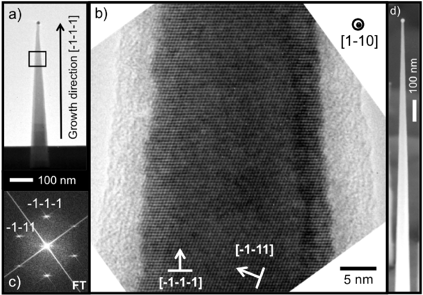
The cone shape of these NWs indicates that, under these growth conditions (low temperature and Te excess), the diffusion length of adatoms on the facets of the NW is not large. Rueda13 This could limit the range of NW length which can be achieved. Nevertheless, NWs grown for a longer time (60 min) exhibit a larger length, as shown in Fig. 2.d. For the same size of the gold droplets, the average diameter at the base of the NWs was increased to , and the length distribution to 0.8-.
The optical properties of single NWs have been characterized by low temperature µPL and CL. ZnTe NWs were first deposited on a patterned silicon substrate by rubbing as-grown samples on the silicon surface. Isolated NWs were identified and precisely located on the substrate using a high-resolution SEM, see Fig. 3.a. Then low temperature (6 K) spectra of these NWS were recorded using a cold-finger cryostat and a confocal µPL set-up. The NWs were excited by W of a cw laser beam focused to on the selected single NW using a microscope objective and a piezoelectric scanner. The light emitted by the NW was collected by the microscope objective and sent to a Jobin-Yvon spectrometer equipped with a CCD camera.
CL images of the same NWs deposited on the silicon substrate were recorded using an FEI Quanta 200 SEM equipped with a CL accessory and a low temperature Gatan stage able to cool down the sample to 6 K. Dona10 The single NW was excited by an electron beam of and a current of typically . In comparison with high resolution field-effect SEM images, the spatial resolution of the CL images is limited by the low spatial resolution of the thermionic SEM. The CL light was collected by a parabolic mirror and sent to an avalanche photodiode synchronized with the electron beam scan.
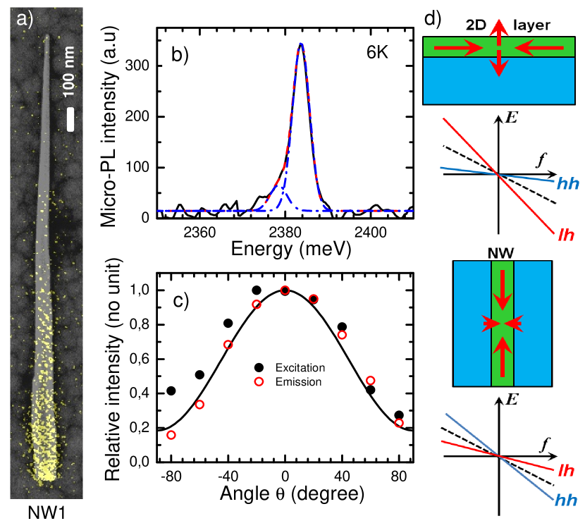
As shown in Fig. 3.b, µPL spectra are dominated by a single emission peak close to the ZnTe exciton band edge. The spectrum has been fitted using two Gaussian lines having a full width at half maximum equal to . The main peak is at , very close to the bulk exciton at : LeSi89 ; Cama02 we will discuss it below as originating from a free or slightly localized exciton. The small satellite peak, observed below the main peak is attributed to bound excitons. Cama02
These results apparently contrast with previous studies performed with ZnTe/(Zn,Mg)Te core-shell NWs, Wojn12 where a band edge emission is observed at . A line at lower energy might be ascribed to trapped excitons or complexes, but the position of the line in the present study, slightly above the exciton in bulk ZnTe, cannot be ascribed to the influence of lateral confinement, which remains negligible for the present range of NW diameters. Indeed such a difference in the exciton energy is expected from the high sensitivity of the band edge emission to the strain induced by the presence of a shell around the NW.
According to Ref. Aifa07, , the stress induced in the core by a lattice mismatched shell covering an infinitely long cylindrical NW is uniform, equal to: Here is the component of the core stress parallel to the NW, and the perpendicular component; is the bulk modulus and is the shear modulus of the core and the shell materials, assumed to have the same isotropic elastic properties; is the lattice mismatch between the core and the shell ( if the shell has a larger lattice parameter); is the core diameter and the external diameter of the core-shell structure. For semiconductor NWs, a more complete calculation,Cibe13 which is beyond the scope of this paper, shows that the previous expressions can be used for oriented semiconductor NWs using the bulk modulus and a shear modulus , where , and are the stiffness coefficients of a cubic semiconductor. This leads to an hydrostatic shift of the band edge emission and a heavy hole-light hole splitting proportional to the lattice mismatch , reduced by the geometrical factor , i.e., the ratio of the shell to the total cross section areas : , and .
For the deformation potentials in ZnTe, we take the values LeSi89 =5.3 eV and =2.5 eV; and for the stiffness coefficients, Berlincourt =73.7 GPa, =42.3 GPa, and =32.1 GPa. Then the excitonic emission of a oriented cubic ZnTe NW is (in meV, with in %) for the heavy hole and for the light hole. The heavy hole is the ground state if , i.e., as noticed in Ref. Wojn12, , if the core is under tensile strain.
For the NWs studied in Ref. Wojn12, , with , , and corresponding to the lattice mismatch between a ZnTe core and a Zn0.8Mg0.2Te shell,Hartmann we obtain for the heavy-hole exciton, in agreement with the observed PL line. One can note that in this core-shell geometry, the position of the heavy-hole emission is more sensitive to the strain than in an epitaxial layer under compressive biaxial strain: the shifts of the heavy-hole state due to the hydrostatic and the shear strain add, while they partially compensate in the epitaxial layer. For the NWs studied in this work, we expect a compressive strain induced by the oxide layer around the NW. For instance, the Zn-Zn distance is 20% smaller in ZnO than in ZnTe. The shell thickness is small, , resulting in a small geometrical factor, less than 0.2. Moreover, the shell is complex, amorphous and probably strongly relaxed. The band edge emission observed at can be interpreted as the influence of a small residual compressive strain on the light hole exciton. Hence, even if the nature of the lines observed in PL here and in Ref. Wojn12, cannot be assessed without a complementary study such as PL excitation or photoconductivity, their position well agrees with the effect expected from the strain induced by the shells.
In Fig. 3.c, we plot the variation of the intensity of the band-edge emission peak when rotating the linear polarization of the laser excitation (solid symbols) or of the detection (open symbols) with respect to the NW axis (determined by SEM, using substrate marks). The maximum of the emission intensity is reached when the polarization is parallel to the NW axis (zero angle). Polarization rates of about 70% are observed for emission and detection, in agreement with the value reported with III-V standing NWs. Zwil09 These effects result from the dielectric screening induced by the characteristic aspect ratio of the NWs. Wang01
For small objects such as the present NWs, the CL excitation efficiency is more than three orders of magnitude lower than the µPL one. The ratio between the electron-hole excitation density in CL experiments and in µPL is given by . Here W/m2 is the mean value of the electrical power density of the CL electron beam when recording a typical image, from which is it generally considered that about one third gives rise to luminescence.Klein68 W/m1 is the laser power density used in the µPL experiment. The excitation in µPL is non-resonant, 160 meV above the ZnTe gap, so that we consider that a good order of magnitude of the absorption by an object of thickness (the NW diameter) is given by , where cm-1 is the value for bulk ZnTe.Langen90 The effect of electrons can be calculated using a Monte-Carlo simulation software (CASINO CASINO ). An incident electron has a very small probability to be scattered inelastically and create an electron-hole pair in the NW; most of its energy is deposited in the substrate where it is scattered many times and propagates randomly. As a result, the creation of electron-hole pairs in the NW is also proportional to D, and much smaller, with an cm-2. This low excitation density prevents any spectral analysis of the CL images for the small NWs studied in this work. Note finally that the CL signal integrated over the NW width corresponds to an energy deposited in the NW proportional to .
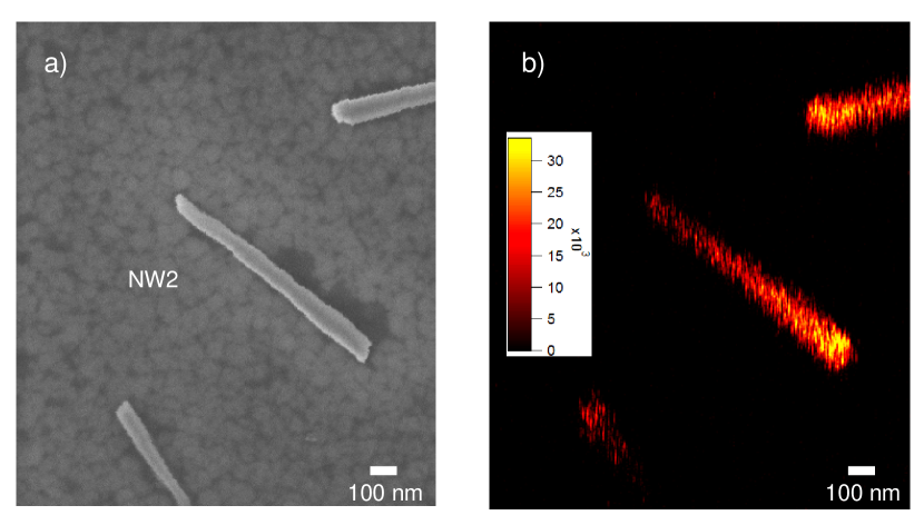
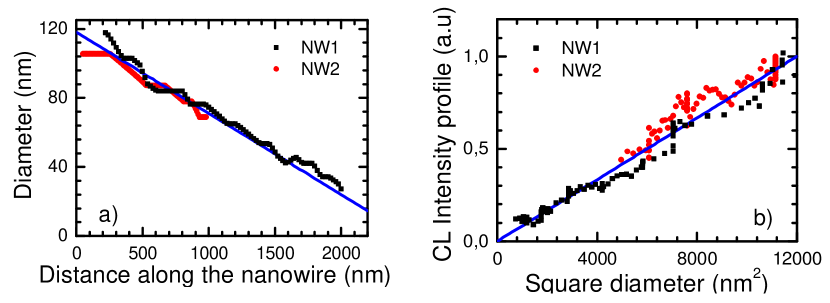
Low temperature, polychromatic CL images were recorded in order to assess the homogeneity of the optical properties. CL emission was systematically observed from the NWs, as shown in Fig. 4.b for the three isolated, broken NWs of Fig. 4.a. For thin cone-shaped NWs like the one labelled in Fig. 3.a, and in Fig 4, the CL intensity decreases from the base to the tip. The local diameter of and , determined from the high resolution SEM images, are shown in Fig. 5.a as a function of the position along the NW. Both NWs display a similar cone shape with the same angle value. Fig. 5.b shows that the CL intensity integrated across the NW diameter at different positions along its axis is proportional to the square of the diameter. This suggests that the radiative efficiency remains constant along the NW, with a CL intensity determined by the excitation density which is proportional to .
To conclude, ultra-low density ZnTe NWs have been grown by MBE at low temperature. These NWs feature a high crystalline quality that is reflected in their optical response. CL of single ZnTe NWs deposited on Si substrates was obtained indicating an homogeneous radiative efficiency along the NWs. Near band edge PL emission was observed from single NWs. A small blue shift (2-3 meV) of the PL energy is attributed to the strain induced by the amorphous oxide layer surrounding the NWs. This assumption is supported by a quantitative calculation of the excitonic shifts induced by strain in core-shell NWs.
Most of this work has been done within the CEA-CNRS joint team “Nanophysique & Semiconducteurs”. We acknowledge the help of the technical teams of Institut Néel, Nanofab (clean room) and Optical Engineering (SEM, S. Pairis), and of J.-P. Poizat. This work is supported by the French National Agency (Magwires, ANR-11-BS10-013).
References
- (1) X. F. Duan, Y. Huang, Y. Cui, J. F. Wang and C. M. Lieber, Nature 409, 66 (2001).
- (2) Z. Fan, D. J. Ruebusch, A. A. Rathore, R. Kapadia, O. Ergen, P. W. Leu, and A. Javey, Nano. Res. 2, 829 (2009).
- (3) Q. F. Meng, C. B. Jiang and S. X. Mao, Appl. Phys. Lett., 94, 043111 (2009).
- (4) S. Bounouar, M. Elouneg-Jamroz, M. den Hertog, C. Morchutt, E. Bellet-Amalric, R. Andre C. Bougerol, Y. Genuist, J.-Ph. Poizat, S. Tatarenko, and K. Kheng, Nano. Lett. 12, 2977 (2012).
- (5) Z. Liu, G. Chen, B. Liang, G. Yu, H. Huang, D. Chen and G. Shen, Opt. Express 21, 7799 (2013).
- (6) P. V. Radovanovic, C. J. Barrelet, S. Gradecak, F. Qian and C. M. Lieber Nano. Lett. 5, 1407 (2005).
- (7) P. Wojnar, E. Janik, L. T. Baczewski, S. Kret, E. Dynowska, T. Wojciechowski, J. Suffczynski, J. Papierska, P. Kossacki, G. Karczewski, J. Kossut, and T. Wojtowicz, Nano. Lett. 12, 3404-3409, (2012).
- (8) A. Bouravleuv, G. Cirlin, V. Sapega, P. Werner, and A. Savin, J. Appl. Phys. 113, 144303 (2013).
- (9) D. Ferrand, J. Cibert, A. Wasiela, C. Bourgognon, S. Tatarenko, G. Fishman, T. Andrearczyk, J. Jaroszynski, S. Kolesnik, T. Dietl, B. Barbara, and D. Dufeu Phys. Rev. B 63, 85201 (2001).
- (10) P. Wojnar, E. Janik, L. T. Baczewski, S. Kret, G. Karczewski, T. Wojtowicz, M. Goryca, T. Kazimierczuk, and P. Kossacki, Appl. Phys. Lett. 99, 113109 (2011).
- (11) L. Besombes, Y. Leger, L. Maingault, D. Ferrand, H. Mariette and J. Cibert, Phys. Rev. Lett. 93, 207403 (2004).
- (12) P. Rueda-Fonseca, E. Bellet-Amalric, P. Stepanov, Y. Genuist, M. Den Hertog, D. Ferrand, K. Kheng, R. André, J. Cibert, and S. Tatarenko, EuroMBE workshop, Levi, Finland (2013)
- (13) A. Ebina, K.Asano, and T. Takahashi, Phys. Rev. B 18, 4341 (1978).
- (14) H. Kirmse, W. Neumann, S. Kret, P. Dluzewski, E. Janik, G. Karczewski, and T. Wojtowicz, Phys. Stat. Sol. (c) 5, 3780 (2008).
- (15) E. Janik, P. Dluzewski, S. Kret, A. Presz, H. Kirmse, W. Neumann, W Zaleszczyk, L.T Baczewski, A. Petroutchik, E. Dynowska, J. Sadowski, W. Caliebe, G. Karczewski, and T. Wojtowicz, Nanotechnology 18, 475606 (2007).
- (16) F. Donatini and Le Si Dang, Nanotechnology 21, 375303 (2010).
- (17) C. A. Klein, J. Appl. Phys. 39, 2029 (1968).
- (18) B. Langen, H. Leiderer, W. Limmer, W. Gebhardt, M. Ruff, and U. Roessler J. Cryst. Growth 101, 718 (1990).
- (19) http://www.gel.usherbrooke.ca/casino/What.html
- (20) Le Si Dang, J. Cibert, Y. Gobil, K. Saminadayar, and S. Tatarenko, Appl. Phys. Lett. 55, 235 (1989).
- (21) J. Camacho, A. Cantarero, I. Hernndez-Caldern and L. Gonzlez, J. of Appl. Phys. 92, 6014 (2002).
- (22) K. E. Aifantis, A. L. Kolesnikova, and E. Romanov, Phil. Magazine 87, 4731 (2007).
- (23) D. Ferrand and J. Cibert, unpublished.
- (24) D. Berlincourt, H. Jaffe, and L. R. Shiozawa, Phys. Rev. 129, 1009 (1963).
- (25) J. M. Hartmann, J. Cibert, F. Kany, H. Mariette, M. Charleux, P. Alleyson, R. Langer, and G. Feuillet J. Appl. Phys. 80, 6257 (1996).
- (26) M. H. M. van Weert, N. Akopian, F. Kelkensberg, U. Perinetti, M. P. van Kouwen, J. Gomez Rivas, M. T. Borgstrom, R. E. Algra, M. A. Verheijen, E. P. A. M. Bakkers, L. P. Kouwenhoven, and V. Zwiller, Small, 5, 21342138, (2009).
- (27) J. Wang, M.S. Gudiksen, X. Duan, Y. Cui, and C.M. Lieber, Science 293, 1455 (2001).