Electron transport across a metal-organic interface
Abstract
We simulate the electron transport across the Au(111)-pentacene interface using non-equilibrium Green’s functions and density-functional theory (NEGF-DFT), and calculate the bias-dependent electron transmission. We find that the electrical contact resistance is dominated by the formation of a Schottky barrier at the interface, and show that the conventional semiconductor transport models across Schottky barriers need to be modified in order to describe the simulation data. We present an extension of the conventional Schottky barrier transport model, which can describe our simulation results and rationalize recent experimental data.
pacs:
73.40.-c, 73.63.-b, 72.10.-d, 72.80.LeI Introduction
Organic materials for electronics is a rapidly growing area, with new commercial organic devices for applications in lighting, displays and photovoltaics being considered. An important problem is the control of charge injection at the metal-organic interface. The charge injection can be associated with a large contact resistance, and is sometimes more dominating for the electrical performance than the transport within the organic semiconductor. The transport across the interface is usually described by the theory of metal-semiconductor contactsIshii et al. (1999); Braun et al. (2009); Kumatani et al. (2013); Liu et al. (2010), where the transport is characterized by an injection barrier that needs to be overcome by thermionic emissionSze (1981). In this paper we show that this theory cannot explain first-principles data of quantum transport across a metal-organic semiconductor interface. Organic semiconductor crystals have much narrower electron bands than ”traditional” inorganic semiconductors, and the theory must be extended to take into account that for certain electron injection energies there may be no available organic crystal bands in the band bending region, and the electron needs to tunnel through this region.
Previous theoretical studies of the metal-organic interface have focused on understanding the properties of a single or few layers of organic molecules on metal surfaces. The focus in this paper is to simulate a true interface between a gold and a pentacene bulk crystal through the use of density-functional theory (DFT) and the non-equilibrium Green’s function (NEGF) method. To our knowledge this is the first study of a single metal-organic interface which does not make use of a slab geometry, but models semi-infinite electrodes by applying open boundary conditions. We show how such simulations can give new insight into the electrostatic properties of the interface, the contact resistance, and electron transport across the interface.
We have chosen the gold-pentacene crystal interface as our model system. Due to its high hole mobility, the pentacene crystal is an important organic electronic material, and the gold-pentacene interface is one of the most well studied systems both theoreticallyPieczyrak et al. (2011); Li et al. (2009); Lee et al. (2007); Lee and Yu (2005); Toyoda et al. (2010); Saranyaa et al. (2012) and experimentally Koch et al. (2007); McDonald et al. (2006); Schroeder et al. (2002); Ihm et al. (2006); France et al. (2003); Käfer et al. (2007); Watkins et al. (2002); Kang and Zhu (2003); Soe et al. (2009); Diao et al. (2007); Liu et al. (2010); Park and Choi (2005), thus there is a large number of experimental and theoretical data for verification of the theoretical simulations.
II Methodology
For all calculations we have used Atomistix ToolKit (ATK) ATK , which is a density-functional theory code that uses numerical localized atom centered basis sets and normconserving pseudopotentials. For the exchange-correlation potential we have used the generalized gradient approximation (GGA) of Wang and PerdewWang and Perdew (1991) (PW91) as suggested by Li et al.Li et al. (2009)
The electronic structure is expanded in basis sets optimized to reproduce hydrogen and carbon dimer total energies following the procedure of Blum et al.Blum et al. (2009) For carbon we use 21 orbitals per atom with , and character and radial ranges up to 3.9 Å, and for hydrogen we use 5 orbitals per atom with and character and ranges up to 4.2 Å. For gold we use a minimal basis set with 9 orbitals per atom and ranges up to 3.6 Å, and add a layer of gold ghost orbitals above the gold surface. With this model we calculate an ionization energy of 6.34 eV (6.589Gruhn et al. (2002)) for pentacene, and a work function of 5.20 eV (5.26Hansson and Flodström (1978)) for the Au(111) surface, where the corresponding experimental values are given in parentheses.
To describe the gold-pentacene interface we correct for basis set superposition errors (BSSE) using the counterpoise correctionLee et al. (2007), and using this computational model with an () k-point grid, we reproduce the geometry, work function change, and adsorption energyStokbro and Smidstrup of pentacene on the Au(111)-( surface obtained with a plane-wave methodLi et al. (2009). In this paper we study pentacene on the Au(111)-( surface. This structure has been observed experimentallyKoch et al. (2007) and the adsorption energy of a pentacene monolayer is higher for this structure compared with the Au(111)-( surfaceStokbro and Smidstrup .
III Results
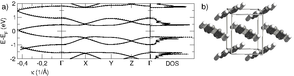
The experimentally observed pentacene crystal geometrySchiefer et al. (2007) is shown in Fig. 1b. To combine the crystal with the Au(111)-( cell, it is necessary to strain the pentacene crystal % in the interface plane. With this constraint on the cell, we then optimize the length of the interface cell in the transport direction and the pentacene coordinates. To investigate the influence of such modifications on the electronic structure we have calculated the complex band structure, band structure and density of states of the pentacene crystal at the experimental lattice constant and compared with the strained crystal. The results are shown in Fig. 1a, where the dotted lines are for the strained case. We see that the electronic structure is almost identical to the unstrained pentacene crystal (solid lines), and thus the straining of the crystal will only have a minor impact on our electron transport calculations.
To set up the geometry of the Au(111)-pentacene interface, we have first relaxed an Au(111)- slab with 2 pentacene layers, until the forces of all pentacene atoms and the first 2 gold layers were below 0.01 eV/Å. We next used the pentacene crystal as a template for extending the slab from 2 to 6 pentacene layers, and relaxed all atoms in layers 2, 3, and 4 until the forces were below 0.02 eV/Å. Finally, we attached semi-infinite electrodes to set up a device configuration as shown in Fig. 2. The BSSE correction cannot be applied in the device configuration, and we can therefore only obtain reliable forces for atoms in pentacene layers 2, 3, and 4. In these layers the forces are below 0.04 eV/Å, confirming that our procedure for generating the geometry using a slab configuration is accurate. In the following we will calculate the properties of this interface.
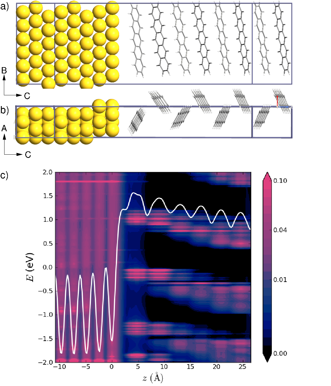
Figure 2c shows the local density of states (LDOS) of the Au(111)-pentacene interface plotted along the transport direction . The 5 gold layers and 6 pentacene layers are visible as positions with large LDOS values. For the pentacene layers we clearly see the molecular levels. We note the shifts in the molecular levels in the direction, corresponding to a band bending in the organic crystal at the interface. The solid white line shows the average electrostatic potential, which exhibits the same band bending behaviour.
Figure 2c also shows how the metallic gold states extend through the adsorbed pentacene molecules into the pentacene crystal. This is seen as an asymmetric shape of the LDOS states, with a long tail at energies above the maximum in the LDOS peak. This is particularly clear for molecules in the 3rd layer above the interface. Thus, the LDOS illustrates the difficulties for the metallic states to propagate through the band bending region into the pentacene electrode.
The band bending is a result of Fermi level pinning of the pentacene highest occupied molecular orbital (HOMO) at the gold-pentacene interface, which shifts the pentacene levels at the interface relative to their positions in the organic crystal electrode. The electronic structure in this (the right) electrode corresponds to an intrinsic pentacene bulk crystal where the Fermi level is in the middle of the band gap. When no bias is applied between the two electrodes, the gold and pentacene Fermi levels are aligned, and the pentacene HOMO band edge in the right electrode is eV below the gold Fermi level. At the interface the HOMO is pinned to the gold Fermi level, thus creating a total band bending of 0.4 eV.
The pinning of the HOMO level arises because the ionization energy of the pentacene crystal is lower than the work function of the gold surface. We calculate a work function of gold of 5.20 eV and an ionization energy of the pentacene crystal of 5.04 eV.
Figure 3b shows the change in the electron density of the gold interface upon adsorption of pentacene. The plot was obtained by subtracting the electron density of the isolated gold and pentacene surfaces from the combined system, and shows the formation of a surface dipole at the interface. Note that this is not a charge transfer from pentacene to gold, since the dipole is located between the top gold layer and the first pentacene layer. The surface dipole arises from the so-called pillow effectKoch et al. (2007), where the pentacene molecule pushes the gold density back.
This surface dipole lowers the workfunction of gold. For a single layer of pentacene on Au(111) we calculate a work function of 4.48 eV, which is in excellent agreement with experimental data (4.52Schroeder et al. (2002) , 4.4Watkins et al. (2002) , 4.6Diao et al. (2007) eV).
We next apply different bias voltages, = -0.4, -0.2, 0.0, 0.2, and 0.4 Volt to the pentacene electrode. The bias will shift the electrochemical potential in the organic electrode by relative to the chemical potential in the metal electrode. Figure 3a shows the electrostatic potential along the -direction for the different bias voltages. The zero-bias potential corresponds to the electrostatic potential of Fig. 2c. A negative bias increases the pentacene electrochemical potential and thereby reduces the band bending, while a positive bias lowers which increases the band bending.
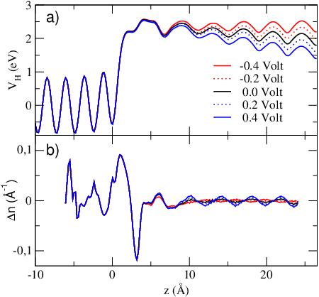
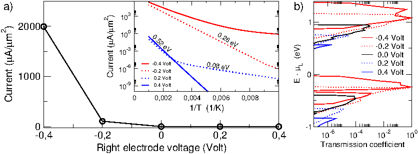
Figure 4a shows the calculated current-voltage characteristics of the interface. The interface shows a strong rectifying behaviour. The inset in the figure also shows the temperature dependence of the current. The temperature dependence shows activated electron transport, meaning that thermionic emission is the dominating current contribution. For each bias the barrier corresponding to the slope of the curve is indicated. In the following we will investigate this in further detail and make a simple model of the transport across the interface.
Figure 4b shows the transmission spectrum as function of the bias voltage applied to the right electrode. The transmission increases exponentially when a negative voltage is applied. At V the maximum transmission is 1, corresponding to a very good coupling between the pentacene crystal and the gold electrode. It follows from the discussion of the band bending above that the system is in flat band condition at this bias voltage, which can also be seen in Fig. 3. For the other computed bias points the bands bend downwards, and a Schottky-type barrier arises at the interface.
In an inorganic semiconductor, a Schottky barrier is reflected by an energy shift of the transmission peaks relative to the metal Fermi level; however, the magnitude of the transmission peaks will not change. For the pentacene crystal, the transmission peaks are both shifted and reduced in magnitude. The reduction is an effect of the band bending of the narrow molecular bands. The band bending is of similar magnitude as the widths of the organic bands, which has the effect that the electron cannot propagate inside a molecular band all the way from the organic crystal to the metal electrode. Outside a molecular band the wavefunction amplitude is exponentially damped with the tunneling distance, thus, for increasing band bending the transmission peak is exponentially lowered.
IV Discussion
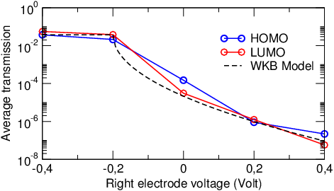
Finally, we present a model that quantifies the reduction of the transmission peaks in the inorganic crystal due to the tunneling through the band bending region. Figure 5 shows the transmission averaged over the HOMO and the LUMO peaks. The curve is flat up to V, and then decreases exponentially. The dashed black line shows a WKB model of the transmission, where the average transmission is given by
| (1) |
In this equation, Å is the distance from the first pentacene layer to the right electrode, and is an effective tunnel barrier, corresponding to vanishing barrier at V and a linearly increasing barrier as a function of .
The total current at bias is given by
| (2) |
where is the transmission coefficient, the Fermi function, the electron temperature, and the Boltzmann constant.
Under forward bias the current can be approximated by
| (3) |
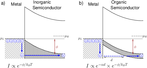
where and is the offset between the semiconductor valence band and the metal chemical potential. For an inorganic semiconductor , but for an organic semiconductor as inferred from Eq. (1).
This qualitative difference in the electron transmission across a metal-semiconductor interface for inorganic and organic systems, respectively, is illustrated in Fig. 6. The model illustrates how the narrow organic crystal bands leads to an additional Schottky barrier contact resistance for a metal-organic interface.
It is interesting to compare this model with the experimental data for transport across the gold-pentacene interface by Liu et al.Liu et al. (2010) They find a large contact resistance and rectification for the gold-pentacene interface, in qualitative agreement with our calculations. (A quantitative comparison is not immediately possible since the effective contact area is unknown in the experiment.) Liu et al. model the data in terms of a traditional Schottky barrier. In order to explain the large contact resistance they suggest that the interface dipole rigidly shifts the bands in the organic semiconductor, which introduces an additional injection barrier. We note, however, that their model assumes a shift of the Fermi level in the organic crystal relative to its HOMO and LUMO bands upon forming the interface with gold, thus, the interface dipole should change the organic crystal from p to n type, which we find unphysical.
Liu et al. also assume band bending at the interface, however, in their case the band bending has no direct electrical effect on the contact resistance. Our model suggests that the band bending will indeed affect the injection probability, thus leading to an alternative model for the large contact resistance which does not require the introduction of an additional injection barrier.
Furthermore, Liu et al. noticed that the metal-organic contact resistance can be reduced by incorporating an inorganic semiconductor buffer layer between the metal and the organic crystalKumatani et al. (2013); Liu et al. (2010). They suggest that the effect of the inorganic semiconductor is to remove the interface dipole and thereby the additional injection barrier. We propose an alternative explanation for this effect. The buffer layer will unpin the HOMO band at the interface, making the organic crystal bands more flat, which increases the electron propagation probability in the band bending region. Thus, unlike models proposed previouslyKumatani et al. (2013); Liu et al. (2010), we suggest that the buffer layers will not change the Schottky barrier, but rather increases the injection probability due to flatter inorganic bands which provides more efficient propagation through the band bending region.
V Summary
In summary, we have studied bias-induced electron transport across the Au(111)-pentacene interface. The study shows that there is a good chemical contact between the gold and the pentacene crystals, and the electrical resistance is dominated by a Schottky barrier within the organic crystal. The transport across the Schottky barrier is thermally activated, however transport is reduced compared to an inorganic semiconductor, since the electron needs to tunnel through part of the band bending region, as illustrated in Fig. 6. Our calculation is a simplification compared to an experimental situation; in particular, the length of the band bending region is orders of magnitude shorter than it is experimentally. However, the calculations suggest an overlooked effect, namely that propagation through the band bending region can be damped due to the narrow bands in the organic semiconductor. We have illustrated how such a model can rationalize recent experimental data for the contact resistance of the gold-pentacene interface and explain the effect of an inorganic buffer layer on the contact resistance.
Acknowledgements.
We acknowledge Alexander Bratkovski for discussions on the metal-organic interface and Anders Blom for proof-reading the manuscript.References
- Ishii et al. (1999) H. Ishii, K. Sugiyama, E. Ito, and K. Seki, Adv. Mater., 11, 605 (1999).
- Braun et al. (2009) S. Braun, W. R. Salaneck, and M. Fahlman, Adv. Mater., 21, 1450 (2009).
- Kumatani et al. (2013) A. Kumatani, P. Dermawan, T. Minari, and K. Tsukagoshi, Scientific Reports, 3, 1026 (2013).
- Liu et al. (2010) Z. Liu, M. Kobayashi, B. C. Paul, Z. Bao, and Y. Nishi, Phys. Rev. B, 82, 035311 (2010).
- Sze (1981) S. M. Sze, Physics of Semiconductor Devices (Wiley, New York, 1981).
- Pieczyrak et al. (2011) B. Pieczyrak, E. Abad, F. Flores, and J. Ortega, J. Chem. Phys., 135, 084702 (2011).
- Li et al. (2009) H. Li, Y. Duan, V. Coropceanu, and J.-L. Bredas, Organic Electronics, 10, 1571 (2009).
- Lee et al. (2007) K. Lee, J. Yu, and Y. Morikawa, Phys. Rev. B, 75, 045402 (2007).
- Lee and Yu (2005) K. Lee and J. Yu, Surf. Sci., 589, 8 (2005).
- Toyoda et al. (2010) K. Toyoda, I. Hamada, K. Lee, S. Yanagisawa, and Y. Morikawa, J. Chem. Phys., 132, 134703 (2010).
- Saranyaa et al. (2012) G. Saranyaa, S. N. V. Natarajanb, P. Kolandaivela, and K. Senthilkumara, J. Mol. Graph. and Mod., 38, 334 (2012).
- Koch et al. (2007) N. Koch, A. Kahn, J. Ghijsen, J. Pireaus, J. Schwartz, R. L. Johnson, and A. Elschner, Appl. Phys. Lett., 82, 70 (2007a).
- McDonald et al. (2006) O. McDonald, A. A. Cafolla, D. Carty, G. Sheerin, and G. Hughes, Surf. Sci., 600, 3217 (2006).
- Schroeder et al. (2002) P. Schroeder, C. B. France, J. B. Park, and B. A. Parkinson, J. Appl. Phys., 91, 3010 (2002).
- Ihm et al. (2006) K. Ihm, B. Kim, T.-H. Kang, K. Kim, M. H. Joo, T. H. Kim, S. S. Yoon, and S. Chung, Appl. Phys. Lett, 89, 033504 (2006).
- France et al. (2003) C. B. France, P. Schroeder, J. B. Forsythe, and B. A. Parkinson, Langmuir, 19, 1274 (2003).
- Käfer et al. (2007) D. Käfer, L. Ruppel, and G. Witte, Phys. Rev. B, 75, 085309 (2007).
- Watkins et al. (2002) N. J. Watkins, L. Yan, and Y. Gao, Appl. Phys. Lett., 80, 4384 (2002).
- Kang and Zhu (2003) J. H. Kang and X.-Y. Zhu, Appl. Phys. Lett, 82, 3248 (2003).
- Soe et al. (2009) W.-H. Soe, C. Manzano, A. DeSarkar, N. Chandrasekhar, and C. Joachim, Phys. Rev. Lett., 102, 176102 (2009).
- Diao et al. (2007) L. Diao, C. D. Frisbie, D. D. Schroepfer, and P. P. Ruden, J. Appl. Phys., 101, 014510 (2007).
- Park and Choi (2005) J. Park and J. S. Choi, Synthetic Metals, 155, 657 (2005).
- (23) The calculations where performed with Atomistix ToolKit, version ATK-12.8, QuantumWise A/S (2012). http://quantumwise.com/documents/manuals.
- Wang and Perdew (1991) Y. Wang and J. P. Perdew, Phys. Rev. B, 43, 8911 (1991).
- Blum et al. (2009) V. Blum, R. Gehrke, F. Hanke, P. Havu, X. Ren, K. Reuter, and M. Scheffler, Computer Phys. Comm., 180, 2175 (2009).
- Gruhn et al. (2002) N. E. Gruhn, D. A. da Silva Filho, T. G. Bill, M. Malagoli, V. Coropceanu, A. Kahn, and J.-L. Brédas, J. Am Chem. Soc., 124, 7918 (2002).
- Hansson and Flodström (1978) G. V. Hansson and S. A. Flodström, Phys. Rev. B, 18, 1572 (1978).
- (28) K. Stokbro and S. Smidstrup, In preparation.
- Schiefer et al. (2007) S. Schiefer, M. Huth, A. Dobrinevski, and B. Nickel, J. A. Chem. Soc., 129, 10316 (2007).
- Koch et al. (2007) N. Koch, A. Volmer, S. Duhm, Y. Sakamoto, and T. Suzuki, Adv. Mater., 19, 112 (2007b).