Ferromagnetism and infrared electrodynamics of Ga1-xMnxAs
Abstract
We report on the magnetic and the electronic properties of the prototype dilute magnetic semiconductor Ga1-xMnxAs using infrared (IR) spectroscopy. Trends in the ferromagnetic transition temperature with respect to the IR spectral weight are examined using a sum-rule analysis of IR conductivity spectra. We find non-monotonic behavior of trends in with the spectral weight to effective Mn ratio, which suggest a strong double-exchange component to the FM mechanism, and highlights the important role of impurity states and localization at the Fermi level. Spectroscopic features of the IR conductivity are tracked as they evolve with temperature, doping, annealing, As-antisite compensation, and are found only to be consistent with an Mn-induced IB scenario. Furthermore, our detailed exploration of these spectral features demonstrates that seemingly conflicting trends reported in the literature regarding a broad mid-IR resonance with respect to carrier density in Ga1-xMnxAs are in fact not contradictory. Our study thus provides a consistent experimental picture of the magnetic and electronic properties of Ga1-xMnxAs.
I Introduction
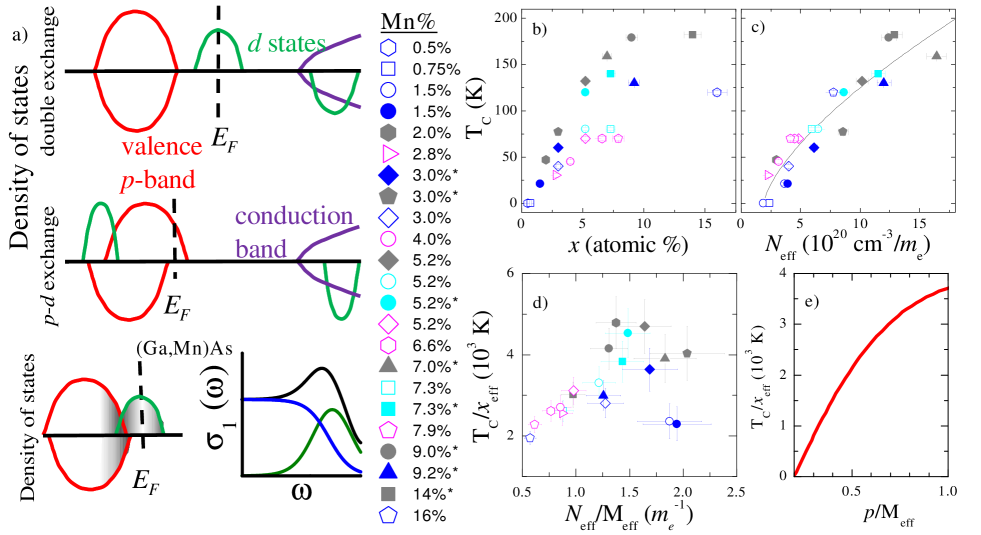
Much of the interest in the ferromagnetic semiconductor Ga1-xMnxAs stems from the rich physics of metallicity ferromagnetism induced in a semiconducting host through doping with magnetic impurities. There is a general consensus that itinerant holes, introduced by the Mn doping, mediate the ferromagnetic interaction between the magnetic moments of the Mn ions Jungwirth et al. (2006); Burch et al. (2008); Sato et al. (2010). Thus all proposed ferromagnetic (FM) mechanisms of Ga1-xMnxAs are intimately tied to the dynamics of the charge carriers. This interplay between the electronic structure and magnetism necessitates studies that can form a comprehensive description of both the observed electronic magnetic properties in a consistent manner. This need is amplified by a long standing controversy regarding the location of Fermi level () in the band structure of FM Ga1-xMnxAs (See reviews by Dietl Dietl (2010), and or Samarth Samarth (2012), for instance). This controversy centers on the character of the states at , as we describe below.
In one scenario, Zener’s double exchange, of which the electronic structure is diagramed in the top panel of Fig. 1a, resides in the partially occupied majority band of Mn impurity states. In this picture, electronic conduction via hopping within the impurity band (IB) mediates the magnetic exchange, with an energy gain controlled by the magnitude of the hopping matrix element for ferromagnetically coupled Mn impurities Anderson (1963); Sheu et al. (2007); Sato et al. (2010). Because this interaction relies on itinerant carriers, there is no energy gain for ferromagnetism if the IB is completely filled or completely empty.
In the alternative Zener’s - exchange scenario (middle panel of Fig. 1a), resides in the exchange split valence band of the host. In this picture hybridization of the impurity wavefunctions with the wavefunctions of the neighboring elements produce level repulsion of the like spins states. Thus the majority spin band is shifted to higher energies, and the minority band is shifted to lower energies. This scenario results in a relatively weak, yet very long ranged interaction that is due to the extended nature of the states of the host valence band (VB) Dietl et al. (2000); Jungwirth et al. (2006).
Double exchange and - exchange are not necessarily mutually exclusive scenarios for the true nature of the interatomic exchange interaction. Rather, double exchange and - exchange may both contribute to the resultant FM ground state of Ga1-xMnxAs. In terms of the magnetic interactions, the IB double exchange and the VB - exchange scenarios are merely the strong-coupling narrow-band limit, and the weak-coupling extended state limit of each other, respectively. Other magnetic exchange interactions may also play a secondary role as well, but these are beyond the scope of this paper (see reviews of Ref. Jungwirth et al. (2006) and Ref. Sato et al. (2010) for a complete profile of magnetic interactions). The crucial point is that the nature of the interaction depends heavily on details of the electronic structure and degree of localization of the mediating holes.
In this work, we experimentally address both the magnetic and the electronic properties of the prototype dilute magnetic semiconductor Ga1-xMnxAs using infrared (IR) spectroscopy. We first examine the relationship between the infrared spectral weight, which is proportional to the carrier density (Eq. 1), and the ferromagnetic transition temperature . This relationship is determined through a sum-rule analysis of our data and additional IR data available in the literature (Refs. Singley et al. (2002); Burch et al. (2006); Jungwirth et al. (2010)) (Sec. II). Our analysis shows the position and degree of localization at plays a key role in controlling (Fig. 1d and discussion in Sec. II). In Sec. IV, we perform a detailed examination of the spectral features observed in the IR data of our Ga1-xMnxAs films, and show that these features are also consistent only with a Mn-induced IB scenario, and that resides in this region. In this latter section, we discuss a connection between the previous experimental findings of Refs. Burch et al. (2006) and Jungwirth et al. (2010), which reported seemingly conflicting trends in the peak frequency of a broad mid-IR resonance with respect to carrier density. By examining trends in with respect to temperature, As:Ga growth ratio, Mn dopant concentration, in both as-grown and annealed samples, our data show that the results of these earlier experiments are in fact not contradictory at all. Moreover, the data is consistent with excitations to Mn-induced impurity states.
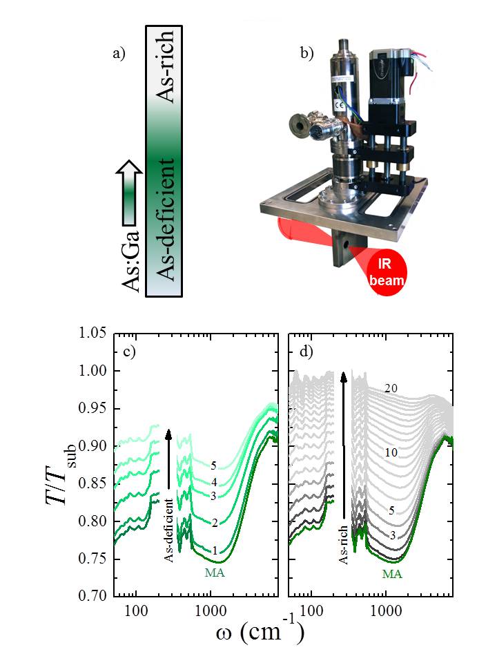
The samples interrogated in our experiments are grown using a “non-rotated” molecular beam epitaxy (MBE) technique. The non-rotated technique aims to reduce or eliminate As antisite (AsGa) compensation through spatial control of the As-flux during growth (Sec. III). Incorporation of compensating defects is the primary limiting factor in minimizing disorder and maximizing in Ga1-xMnxAs. The most prevalent compensating defects are Mn-interstitials (Mni), and As-antisites (AsGa), both of which are double donors Erwin and Petukhov (2002); Missous (1994). These defects are an unintentional result of the low growth temperatures necessary to achieve Mn concentrations sufficient for ferromagnetism and to suppress the formation of secondary phases (e.g. MnAs) Ohno et al. (1996).
Post-growth annealing at relatively low temperatures has been shown to reduce Mni because of their high diffusivity, therefore increasing the hole density Edmonds et al. (2004); Ku et al. (2003). The AsGa defects cannot be removed via annealing at temperatures below 500 . Such high annealing temperatures are impractical, however, because at these temperatures Mn also precipitates out to form MnAs nanoparticles Boeck et al. (1996). The necessity for high temperature annealing to reduce As has been circumvented by a “non-rotated” growth technique with spatial control of the As-flux (Sec. III), which results in a film with a corresponding AsGa gradient Myers et al. (2006). Investigating films grown by this technique, the authors of Ref. Myers et al. (2006) have shown that this precise control of the As-flux leads to the systematic reduction (or elimination) of AsGa along the gradient.
The gradient composition of these samples results in a location along the film where AsGa defects have been minimized or eliminated (see Fig. 2). Thus by experimentally probing this optimized location in a film, we obtain data representative of a relatively “clean” sample. Data from the optimized location in our films are reported, for instance, in our analysis of ferromagnetism in Sec. II. Samples grown using the non-rotated technique can provide additional pertinent information through investigation of systematic changes to the IR conductivity spectra () of Ga1-xMnxAs films along the As:Ga gradient. Tuning the material properties in this manner, and tracking the evolution of the spectroscopic features across the AsGa gradient, yields a detailed picture of the electrodynamics of Ga1-xMnxAs. Therefore our infrared study, combining an infrared spectral weight analysis of ferromagnetism and the systematic study of the infrared spectral features, serves as a unique endeavor to use a single experimental technique to address both the electronic and magnetic properties of this prototype FM semiconductor.
To further establish that the electrodynamics of FM Ga1-xMnxAs is distinct from genuine metallic behavior due to extended states in the host VB, we also examine an =0.009 Ga1-xBexAs sample grown using the same non-rotated technique. This is an ideal system to compare and contrast with the electrodynamics of Ga1-xMnxAs, as substitutional Be also forms a single acceptor state in GaAs, however, without the accompanying magnetic moment. The Ga0.991Be0.009As sample displays conventional metallicity with spectroscopic features consistent with transport in the host VB, in contrast to that of Ga1-xMnxAs.
The paper is organized as follows. First, we present our analysis of the relationship between the IR spectral weight and in Sec. II. Following that, we provide details of our samples and experimental methods in Sec. III. Sec. IV covers the IR conductivity spectra of our -doped GaAs films, Ga1-xMnxAs and Ga1-xBexAs. This latter sections examines the dependence of the spectra on the As:Ga growth ratio in both Ga1-xMnxAs and Ga1-xBexAs, and on the doping dependence in Ga1-xMnxAs. Discussion of the trends of is also found in Sec. IV. Finally, concluding statements are found in Sec. V.
II An infrared perspective on trends in
In Fig. 1b we plot as a function of dopant concentration of all the Ga1-xMnxAs samples in our analysis. The samples include as-grown films investigated by Singley Singley et al. (2002), as-grown and annealed films of Burch Burch et al. (2006), annealed films of Jungwirth Jungwirth et al. (2010), and the non-rotated as-grown and annealed samples of this work (see Table 1). For the later samples presented in Fig. 1, only the optimized location along the As:Ga gradient is reported in the figure (method for determination of this location is found Sec. IV.1). In these works, the total Mn concentration was determined by electron microprobe analysis (Refs. Singley et al. (2002); Burch et al. (2006)), measuring the ratio of beam equivalent pressures of Mn and Ga sources before each growth (and cross checked on several samples using secondary ion mass spectroscopy) (Ref. Jungwirth et al. (2010)), and growth rate calibrations of MnAs and GaAs reflection high-energy electron diffraction (RHEED) oscillations (this work). The totality of the data in Fig. 1b show no clear systematic trend across the doping profile, and non-reproducible for samples of the same nominal dopant concentration. These observations highlight the difficult nature of predicting based on Mn-concentration alone in this defect prone material.
The relationship between carrier density and , as opposed to and , can provide a more insightful picture into the nature of magnetism in this carrier mediated ferromagnet. IR experiments serve as a contactless method sensitive to the carrier density through the sum-rule given by
| (1) |
The “spectral weight” is proportional to the effective number of charges contributing to electromagnetic absorption at frequencies below . Therefore Eq. 1 establishes the relationship between the spectral weight and the charge density . When Eq. 1 is applied to a feature originating from an interband process, is the reduced mass of the bands involved Dressel and Grüner (2002). When Eq. 1 is applied to a spectral feature arising from an intraband process, is the effective mass of the relevant band. If Eq. 1 is integrated over multiple features arising from distinct processes, will be a “mixture” of the effective masses of each of the excitation processes contributing to the spectrum below .
In Fig. 1c we plot as a function of in the Ga1-xMnxAs samples. We use =6450 cm-1 as the integration cut-off in order to rule out any significant contribution from excitations into the GaAs conduction band. Moreover, this cut-off is well established in these materials and facilitates direct comparison with other studies in the literatureSinova et al. (2002); Burch et al. (2006); Chapler et al. (2011). As can be seen in the figure, while the data do not perfectly collapse onto a singlular trend line, there is an overall trend indicating that increasing increases . The trend in Fig. 1b is indicated by a power law fit (black line) of all the data points, which finds an exponent of 0.67.
Remarkably, the overall trend in Fig. 1c is evident despite the fact that there was no clear trend in versus (Fig. 1b), and despite the fact that the samples in Fig. 1 span a wide variety of Mn doping levels and growth procedures, including different thicknesses, rotated and non-rotated growths, and as-grown and annealed samples (Table 1). The data of Fig. 1b seemingly confirms earlier results of Ref. Ku et al. (2003), which also found an empirical relationship between and in Ga1-xMnxAs, apparently independent of other physical parameters (though scaled as rather than as found here). These earlier results, however, relied on a deconvolution of coupled optical phonon-plasmon modes in Raman spectra. Our result is achieved in a more straightforward manner, as a simple integration of the intragap spectra weight from our IR conductivity. The overall trend in Fig. 1c suggests a strong relationship between and , which is encouraging given that ferromagnetism in Ga1-xMnxAs is widely agreed upon to be carrier mediated. Another encouraging aspect of Fig. 1c is that up to the largest measured spectral weight ( cm), there are no signs that the trend of increasing is saturating.
One obvious detail missing in any analysis of as a function of only, such as that described above for the data of Fig. 1c, is the concentration of Mn moments, which of course are necessary for ferromagnetism. Thus we are interested in estimating the effective Mn concentration of our samples. Out of the total Mn concentration , the Mn will reside either in substitutional positions or interstitial positions, therefore , where is the concentration of MnGa and that of Mni. Both theory and experiments suggest that Mni–MnGa pairs couple antiferromagnetically Blinowski and Kacman (2003); Mašek and Máca (2004); Edmonds et al. (2004); Bouzerar et al. (2005); Takeda et al. (2008); Zhu et al. (2007), therefore the effective Mn concentration contributing to ferromagnetic order is then . Mni are also considered to be double donors Erwin and Petukhov (2002); Missous (1994), compensating the intentional hole doping of MnGa. Through this latter fact, and by invoking the relationship between the carrier density and the spectral weight established in Eq. 1, we can write that , where is the GaAs lattice constant (for simplicity we have assumed the concentration of AsGa is zero). Putting these relations together, we arrive at our estimate of effective Mn concentration .
For in our equation of , we choose to be in the range of the effective VB mass, placing it from 0.3–0.4 . This choice was guided by IR experiments on (Ga,Mn)As-based electric field effect devices Chapler et al. (2012). These latter experiments found, noting that is dominated by the VB mass the integration limit in the sum-rule (Eq. 1) is on the order of several thousand wavenumbers in (Ga,Mn)As, that Mn dopoing does not lead to substantial renormalization of the GaAs host VB. This result on field effect devices is in accord with the analysis of resonant tunneling spectroscopy experiments in (Ga,Mn)As layers as well Ohya et al. (2011a). It is worth noting that the maximum such that for all the samples in Fig. 1 is 0.8 . Using this maximum value of does not change the qualitative behavior of the data in Fig. 1e, which we discuss in the following paragraphs.
Having obtained an estimate of , we plot versus /Meff, where Meff is the density of effective Mn moments (M) in Fig. 1d. The value of /Meff gives an approximation of the relative degree of compensation of each film. For /M1.25 , these data show a monotonic increase in for increasing /Meff. This general trend is expected in both a - exchange scenario Jungwirth et al. (2005), as well a double-exchange scenario Sato et al. (2010) for Ga1-xMnxAs. For /M1.25 , the data seem to be maximized in a range of roughly 1.3 /M1.6 . We note the film with the highest (182 K) falls within this latter range, while the film with the second highest (179 K) falls within the former range. Continuing to higher values of /Meff, the data then show either a plateaued or decreasing trend, which is not easily discerned given the error bars. However, the =0.015 samples show a significant overall decrease in , displaying a suppression of over 50%, while having among the largest values of /Meff.
The theoretical curve of versus /Meff calculated in Ref. Jungwirth et al. (2005) is displayed in Fig. 1e. This curve is based on an electronic structure, calculated using a microscopic tight-binding approximation, in which the valence and impurity bands of Ga1-xMnxAs have completely merged. The ferromagnetic properties are thus calculated according to a semiphenomenological - exchange mean-field approximation. The key theoretical prediction of Ref. Jungwirth et al. (2005), is a systematic, monotonically increasing trend in , with a corollary that the highest will occur for films with close to zero compensation. Furthermore, to the best of our knowledge, all VB - exchange descriptions predict a monotonic increase of with both and .
According to our IR spectral weight analysis, the key prediction made in the - exchange framework (monotonic increase of ) is not in agreement with the data. Non-monotonic trends of have also been reported in Ref. Dobrowolska et al. (2012) using a simultaneous combination of channeling Rutherford backscattering (c-RBS) and channeling particle-induced X-ray emission (c-PIXE) Dobrowolska, M., Liu, X., Furdyna, J. K., Berciu, M., Yu, K. M., Walukiewicz (2012). In contrast, high-field Hall measurements of the carrier density do not show the non-monotonic behavior seen in Fig. 1d Jungwirth et al. (2005). The experimental data of Refs. Dobrowolska et al. (2012) and Jungwirth et al. (2005) have both been disputed Edmonds, K. W., Gallagher, B.L., Wang, M., Rushforth, A. W. Makarovsky, O. Patane, A. Campion, P., Foxon. C. T., Novak, V., Jungwirth (2012); Dobrowolska, M., Liu, X., Furdyna, J. K., Berciu, M., Yu, K. M., Walukiewicz (2012). With this noted disagreement in the literature, we emphasize that our experiments are done using a technique entirely different from any of those above. Furthermore, our IR method is a contactless probe, and the sum-rule analysis is based on model-independent arguments that are rooted in the causality of the electromagnetic response Basov et al. (2011). We reiterate that the highest films (182 K and 179 K) displayed in Fig. 1 (filled gray square and circle, respectively) have spectral weight that is well below that expected for the uncompensated case, which is contradictory to the predictions of the - exchange mean-field approximation. Therefore, we argue that the ferromagnetic properties of Ga1-xMnxAs require description beyond Zener’s - exchange model.
To our knowledge, there is no microscopic theory that has presented a quantitative description of the non-monotonic behavior of Fig. 1d. It was argued in Ref. Dobrowolska et al. (2012) that is controlled by the location of in a Mn-induced IB. From the basis of tight-binding Anderson calculations, however, IB models used to describe earlier experiments Burch et al. (2006); Stone et al. (2008); Ando et al. (2008); Tang and Flatté (2008) fail to demonstrate how the IB could remain sufficiently narrow as to avoid overlap with the VB at the doping levels necessary to initiate FM Mašek et al. (2010). A strictly detached IB, however, is not theoretically necessary for the qualitative behavior seen in Fig. 1d. First principle investigations of the electronic structure and magnetism find Ga1-xMnxAs to be an intermediate case, with contributions to ferromagnetism coming from both --like and double exchange-like mechanisms. The calculated DOS of this later study finds significant merging of the IB and VB, yet still with a large amplitude of states at , a corresponding suppression of as a function of increased hole concentration Sato and Dederics (2003). These same techniques when applied to other dilute magnetic semiconductors show the dome-like behavior of typical of a double exchange FM mechanism becomes further pronounced in cases where the separation of the IB and VB are more distinct, e.g. Ga1-xMnxN.
The non-monotonic nature of the data of Fig. 1d shows that the FM mechanism of Ga1-xMnxAs has a strong double-exchange component. This fact highlights the important role played by impurity states and localization at . A schematic representation of the DOS consistent with our data is shown in the bottom panel of Fig. 1a. Although this schematic lacks subtleties that may vary with parameters such as the Mn concentration and compensation in real materials, a generic optical conductivity lineshape (bottom right panel of Fig. 1a) has been observed in all FM Ga1-xMnxAs samples of the studies represented in Fig. 1. This latter fact implies spectroscopic features and carrier dynamics in FM Ga1-xMnxAs films reported in the literature originate from the same basic physical picture, despite variations in the growth and film preparation procedures across these works. Furthermore, detailed spectroscopic probes of the IMT in GaMnAs reveal that the generic picture of the DOS in bottom panel of Fig. 1a holds over a wide range of Mn concentrations, persisting over an order of magnitude of Mn doping beyond the onset of conduction in FM Ga1-xMnxAs Chapler et al. (2011). In Sec. IV, we expand upon the earlier IR data and further demonstrate that the generic spectral features oberved in Ga1-xMnxAs persist over a wide parameter space, and are consistent with an IB scenario.
| Reference | nominal doping (%) | thickness (nm) | TC (K) |
|---|---|---|---|
| Ref. Singley et al. (2002) | 2.8 | 500 | 30 |
| 4.0 | 500 | 45 | |
| 5.2 | 500 | 70 | |
| 6.6 | 500 | 70 | |
| 7.9 | 500 | 70 | |
| Ref. Burch et al. (2006) | 5.2 | 40 | 80 |
| 5.2* | 40 | 120 | |
| 7.3 | 40 | 80 | |
| 7.3* | 40 | 140 | |
| Ref. Jungwirth et al. (2010) | 2.0* | 20 | 47 |
| 3.0* | 20 | 77 | |
| 5.2* | 20 | 132 | |
| 7.0* | 20 | 159 | |
| 9.0* | 20 | 179 | |
| 14* | 20 | 182 | |
| This work | 0.5 | 200 | 4 |
| 0.75 | 200 | 4 | |
| 1.5 | 200 | 21 | |
| 1.5* | 200 | 21 | |
| 3.0 | 200 | 42 | |
| 3.0* | 200 | 60 | |
| 9.2* | 100 | 130 | |
| 16 | 100 | 120 |
III Samples and experimental methods
III.1 Sample growth and characteristics
All films in this study were prepared via MBE, on semi-insulating (001) GaAs substrates. The films were prepared using the non-rotated, low-temperature growth techniques reported in Refs.Myers et al. (2006); Mack et al. (2008). Since this study involved several doping regimes, details of the growth vary between samples. Specific details on the film preparation of all samples can be found in Table 2. In the Ga1-xMnxAs samples, the Mn dopant concentration was determined by growth rate calibrations of MnAs and GaAs RHEED oscillations. For the Ga0.991Be0.009As sample, the Be concentration was determined from room temperature Hall-effect data.
The non-rotated technique utilizes a geometry in which the MBE system provides a continuous variation in the As:Ga ratio in one direction along the wafer. This yields precise control over the density of AsGa, while holding Mn (or Be) flux approximately constant Myers et al. (2006). Local transport studies along the As:Ga gradient demonstrate that increasing the AsGa density reduces the hole density , mobility and dc conductivity in Ga1-xMnxAs Myers et al. (2006). Additionally, AsGa also affects , magnetization, and magnetic hysteresis curves in FM samples Myers et al. (2006); Mack et al. (2008). These studies show that the location of minimum AsGa density, defined by the location of maximum found along the As:Ga gradient, also corresponds to the region where all of the above properties are optimized. We note, detailed studies of Ref. Myers et al. (2006) have concluded full dopant incorporation is not achieved in the As-deficient regions. In the “optimized” and As-rich regime, however, the data indicate relatively constant Mn concentration (within 0.1% variation) along the As:Ga gradient Myers et al. (2006). In the heavily alloyed samples (=0.092* and 0.16 Mn (* indicates the sample was annealed)), this latter statement is only true for a small region near the optimal location Mack et al. (2008).
Ga1-xMnxAs samples of x=0.005, 0.0075 were found to be paramagnetic (PM) at all locations along the films. The other more heavily doped Ga1-xMnxAs films were found to be FM, with in the region of minimized compensating defects (referred to as MA, with this naming convention explained in Sec. III.2 below) listed in Table 2. The =0.015*, 0.03*, and 0.092* Ga1-xMnxAs samples were also subjected to low-temperature annealing. The =0.015 and 0.015* Ga1-xMnxAs film are the same sample pre- and post-annealing; the same is true for the =0.03 and 0.03* Ga1-xMnxAs film. In the =0.015* and 0.03* samples, after annealing was determined by the temperature of maximum low-frequency resistivity (=1/(40 cm-1)) Chapler et al. (2011)(see Fig. 5i). For all other samples, including =0.015 and =0.03 before annealing, was measured by SQUID magnetometry.
| dopant | % | thickness (nm) | growth () | annealing () |
|---|---|---|---|---|
| Mn | 0.5 | 200 | 250 | - |
| 0.75 | 200 | 250 | - | |
| 1.5 | 200 | 250 | - | |
| 1.5* | 200 | 250 | 220 | |
| 3.0 | 200 | 220 | - | |
| 3.0* | 200 | 220 | 200 | |
| 9.2* | 100 | 200 | 180 | |
| 16 | 100 | 150 | - | |
| Be | 0.9 | 100 | 250 | - |
III.2 Experimental methods
In order to characterize the effects of the As:Ga gradient on the optical properties, we developed a broad-band (far-IR to near-ultraviolet) microscope compatible with low-temperature (20 K) operation (Fig. 2b). Our experimental set-up incorporates a 4x beam condenser and linear translation stage in a Fourier transform IR spectrometer to obtain frequency dependent transmission spectra. The spatial resolution of the apparatus is below 1 mm, which is appropriate for the series of films investigated here. This assertion was validated through direct mid-IR transmission microscopy experiments, with the IR-beam diameter focused to less than 100 m at the sample, taking measurements in 1 mm increments along the As:Ga gradient. The micro-transmission data was supplemented with room temperature micro-ellipsometry measurements for several films (=0.005, 0.0075, 0.015, 0.03, 0.16 Mn and =0.009 Be). The ellipsometry data span a frequency range of 6,000 cm 40,000 cm-1, with spatial resolution 150 m.
Characteristic transmission data along the As:Ga gradient are displayed in Figs. 2c and d. The figures show room temperature transmission through the x=0.005 Ga1-xMnxAs sample, normalized to that of the GaAs substrate. We identify the location of maximum , as the position corresponding the maximum absorption along the sample, and thus refer to this location as MA. A more rigorous and quantitative determination of the location of maximum is completed via optical sum rules (Eq. 1), as detailed later in the manuscript (Sec. IV.1). With this definition of the MA point, the spectra can be divided into two regimes: As-rich, and As-deficient. Spectra in the As-deficient regime show a rapid increase in overall transmission as the IR probe moves deeper into the deficient regime. Detailed studies reported in Ref. Myers et al. (2006) have concluded full dopant incorporation is not achieved in the As-deficient regions. A reduction in dopant concentration is consistent with the decreased absorption observed. Thus, the IR studies in this work focus on the As-rich and MA positions of the samples. In these latter locations, a systematic increase in the overall transmission is observed as the IR beam is moved from MA deeper into the As-rich region. The increase of transmission in the As-rich regime is consistent with reduction in due to AsGa compensation.
Spectroscopic data at frequencies beyond the fundamental GaAs band gap were obtained via ellipsometry measurements. Ellipsometry measures the ratio of the complex reflectivity coefficient () of - and -polarized light. The experimental observables are the ellipsometric angles and according to,
| (2) |
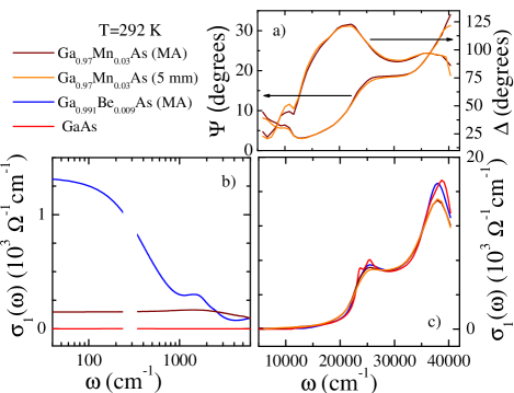
where the subscripts and denote the incident polarization. Fig. 3a shows representative data of our micro-ellipsometry experiments for the =0.03 Ga1-xMnxAs film at the MA position.
To develop a quantitative understanding of the optical data, it is instructive to express the our observables in terms of the complex IR conductivity spectrum )=)+i. We extract the complex conductivity spectrum from our optical data via multi-oscillator modeling. For this model, we use only Kramers-Kronig (KK) consistent oscillators and perform a simultaneous fitting of both the transmission and ellipsometric data. In this way, we construct a KK consistent model of ) over the entire experimental range. Modeling the data over such a large experimental frequency range assures a high degree of confidence in the uniqueness and accuracy of each experimental fit Burch et al. (2004); Kuzmenko (2005). We focus on the real part of the conductivity spectrum, , describing the dissipative processes in the system. Fig. 3b and c display representative plots illustrating extracted by the simultaneous fitting of the room temperature transmission spectrum and ellipsometric data as described above. The data are displayed for the Ga0.97Mn0.03As and Ga0.991Be0.009As samples at MA, both in the intragap region (Fig. 3b), as well as frequencies extending above the fundamental GaAs band gap (Fig. 3c). Further discussion of the spectroscopic features in the intragap regime are found in Sec. IV.
IV Intragap response of -doped Galium Arsenide
IV.1 Carrier density gradient
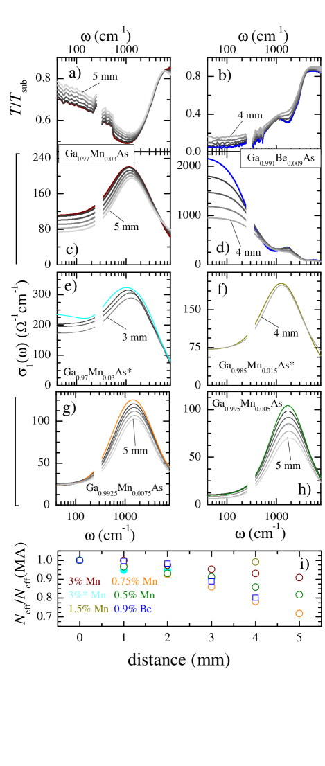
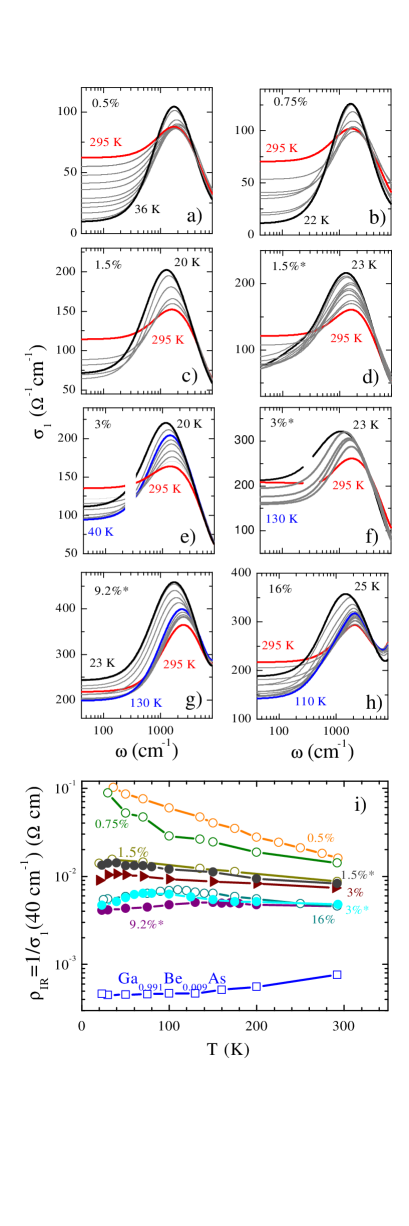
Figs. 4a–d show representative transmission spectra and corresponding for the Ga0.97Mn0.03As and Ga0.991Be0.009As samples. These panels highlight the equivalence of the location along the As:Ga gradient of maximum absorption in the transmission spectra, to that of the maximum in overall . Therefore the MA location can be determined by the position along the As:Ga gradient that displays the maximum spectral weight (Eq. 1). Figs. 4e–h show the intragap data of the other gradient samples measured in this study. Data along the As:Ga gradient of the heavily alloyed samples (=0.09 and 0.16 Ga1-xMnxAs) are not reported because it has been determined that quality surfaces and interfaces are only found in a narrow region near MA Mack et al. (2008). The effect of the As:Ga gradient in terms of the spatial location is quantified in Fig. 4i by the spectral weight , normalized to at MA for each sample (absolute scale for can be read off of Fig. 6c) . Fig. 4i demonstrates suppression of as As content increases past the optimal concentration to be a generic result for the -doped GaAs samples of this study.
Figs. 4a–h demonstrate that the qualitative features of the spectra, although different for Be and Mn-doped samples, are not radically modified by additional AsGa compensation. Ga1-xMnxAs spectra, both at MA and several mm into the As-rich regime, reveal a lineshape consisting of a broad mid-IR resonance and relatively flat conductivity in the far IR. In the Ga1-xBexAs data of in Fig. 4, the spectra at MA and in the As-rich region are dominated by a pronounced low-frequency response. This latter peak can be modeled semi-classically as a Drude peak, given by:
| (3) |
The Drude peak is characteristic of a free carrier response in a metal or degenerate semiconductor, with the amplitude equal to the dc conductivity and the width of the peak quantifying the free carrier scattering rate . As can be seen in the figure, the increase of AsGa in the As-rich region of Ga1-xBexAs suppresses the Drude conductivity and broadens the Drude width. A narrow mid-IR resonance is also suppressed and broadened in the As-rich regions.
IV.2 Doping dependence
The temperature dependence of for all the Ga1-xMnxAs samples in this study at MA are shown in Fig. 5. We observe a qualitatively similar lineshape at all Mn-dopings (see Fig. 1a). The far-IR conductivity, attributed to the itinerant carrier response, is nearly completely suppressed at the lowest temperatures in the PM samples (1%). This vanishing conductivity supports the notion that these samples reside on the insulating side of the Ga1-xMnxAs insulator-to-metal transition (IMT). In these insulating samples, the observed broad mid-IR resonance in the vicinity of Mn-acceptor binding energy has a natural assignment of VB to IB transitions.
The persistence of the far-IR conductivity down to the lowest temperatures in Ga1-xMnxAs samples of 0.0075 reveals films in this dopant regime to be beyond the onset of conduction. However, the onset of conduction in Ga1-xMnxAs remains distinct from genuine metallicity, as can be seen in Fig 5i. In this panel, we plot the temperature dependence of the “infrared resistivity” (=1/(40 cm-1)). The data in the dilute Mn-doped samples (=0.005, 0.0075) show the systematic increase in expected in the case of thermally activated transport. The insulating behavior of these samples down to the lowest temperatures measured establishes the Ga1-xMnxAs films in this doping regime as below the onset of conduction.
The onset of conduction is marked by the finite in the limit of , 0, exhibited by the Ga1-xMnxAs films of 0.0075. Nevertheless, the of the films in this latter dopant regime still display signs of activated transport above . The onset of ferromagnetism radically alters the temperature dependence of and , as below the activated character is reversed. An anomalous increase of the low energy spectral weight with the development of magnetization has also been demonstrated in earlier work on Ga1-xMnxAs Hirakawa et al. (2002); Singley et al. (2002); Chapler et al. (2011), In1-xMnxAs Hirakawa (2001), as well as a canonical double-exchange material La1-xSrxMnO3 Okimoto et al. (1995); Basov et al. (2011). This “mixed” behavior of insulating and metallic trends underscores the unconventional nature of conduction in Mn-doped GaAs beyond the IMT boundary, and serves as a signature of the deep bond between magnetism and the carrier dynamics. Moreover, it establishes the distinction between the onset of conduction and genuine metallicity, the latter of which we now describe below for Ga0.991Be0.009As.
The room temperature spectrum of Ga0.991Be0.009As (blue curve in Fig. 3c) reveals a pronounced Drude peak, and a narrow mid-IR resonance. Upon cooling to 25 K, the Drude peak sharpens and increases in amplitude, typical of genuinely metallic behavior, as does the mid-IR resonance (compare blue curves of Figs. 3b and 4d). The temperature dependence of for this film reveals a metallic trend throughout the entire measured temperature range (Fig 5c). The pronounced Drude peak and metallic temperature dependence establish the genuine metallicity of this film, in contrast with the mixed behavior of Ga1-xMnxAs beyond the onset of conduction. Furthermore, much weaker far-IR spectral weight is found in Mn-doped samples than that of the Be-doped film Chapler et al. (2011).
The carrier density can be readily measured by the Hall effect in the non-magnetic Ga0.991Be0.009As system. From this fact, and coupled with the prominant Drude peak the effective carrier mass can be determined from Eq. 1. This effective mass and was found to be 0.29 at MA for the Ga0.991Be0.009As sample. This value of the carrier mass is supported by the mass extracted from mobility data of -type GaAs doped with nonmagnetic (Zn, C, or Be) acceptors Alberi et al. (2008). Moreover, is in good agreement with the two-band transport mass of light and heavy holes in the GaAs VB of 0.38 Wiley and DiDomenico Jr. (1970). The combination of the light effective carrier mass and metallic temperature dependence of the Drude peak are strong evidence that the IR spectra of the Ga0.991Be0.009As film are representative of the IR response of carriers that reside in extended states of the GaAs host VB.
Decoupling the delocalized Drude-like contributions to the spectra from interband transition contributions limit analysis similar to that above for estimating carrier masses in Ga1-xMnxAs. However, reasonable estimates reveal the effective mass of carriers in Ga1-xMnxAs to be significantly larger than that of the metallic Be-doped sample. The large mass of charge carriers in Ga1-xMnxAs are apparent from the much weaker far-IR spectral weight in Ga1-xMnxAs samples with similar doping to that of the Be-doped film. We further note that the weak far-IR spectral weight of Ga1-xMnxAs samples extends to films with over an order of magnitude higher dopant concentration than the Ga0.991Be0.009As film. More detailed quantitative analysis of Ga1-xMnxAs effective masses in IR data can be found in Ref. Singley et al. (2003); Burch et al. (2006). The relatively large carrier mass is indicative of transport within a narrow band of impurity character. Moreover, the weak far-IR conductivity and coexistence of insulating and metallic trends in the temperature dependence establish that descriptions of electronic conduction in Ga1-xMnxAs require an emphasis on localization. These latter characteristics are distinct from extended states in the VB, and are in line with proposed theories of IR conductivity of Ga1-xMnxAs Moca et al. (2009); Bouzerar and Bouzerar (2011).
IV.3 Mid-IR peak
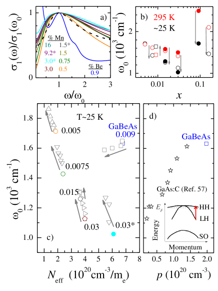
In the discussion above, we demonstrated the notable differences in the far-IR behavior of the spectrum of Ga0.991Be0.009As to that of Ga1-xMnxAs. Thus it is interesting to note there is a mid-IR resonance in Ga0.991Be0.009As with center frequency similar to that of the broad resonance observed in the Ga1-xMnxAs spectra. We argue, however, these features stem from different origins. To highlight the difference between the mid-IR feature in Ga0.991Be0.009As and that of Ga1-xMnxAs, we plot “scaled” conductivity spectra (of the MA location) in Fig. 6a. The figure shows normalized along the axis by the value of the conductivity at the peak frequency () of the broad mid-IR resonance in the Ga1-xMnxAs, and the narrow mid-IR resonance in Ga0.991Be0.009As film, respectively. Along the axis, the spectra are normalized by of each film.
The data in Fig. 5 demonstrate that all the Mn-doped samples (both in the insulating regime and those past the onset of conductivity) show very broad, structureless resonances at mid-IR frequencies. Furthermore, upon scaling of these data (Fig. 6a), the Mn-doped samples reveal a nearly identical lineshape, barring small non-monotonic differences in the width of the mid-IR resonance. The similar lineshape suggests a similar origin of the mid-IR resonance in both insulating and conducting samples (VB to IB optical excitations).
The persistence of the mid-IR resonance in Ga1-xMnxAs samples on the insulating side of the IMT, where an IB is expected for Ga1-xMnxAs and non-controversial Moriya and Munekata (2003); Jungwirth et al. (2007), to samples well above the onset of conductivity, is key evidence that impurity states maintain a prominent role in FM Ga1-xMnxAs. We add to this evidence by calculating the lineshape for VB to IB transitions in Ga1-xMnxAs according to the quantum defect method for band-to-acceptor transitions Bebb (1967) (black dashed line in Fig. 6a). This model was first applied to absorption in semiconductors by Bebb Bebb (1969), and later used to model absorption in magnetic semiconductors such as Cd1-xMnxTe Huber et al. (1987) and Ga1-xMnxAs Kojima et al. (2007). The details of our calculation can be found in Ref. Chapler et al. (2011). Evident in Fig. 6a is that the lineshape calculated by the quantum defect method is in good agreement with the lineshape of the mid-IR resonance observed in the Ga1-xMnxAs samples. More complex calculations of VB to IB transitions in Ga1-xMnxAs have also been shown to capture key aspects of the experimentally observed mid-IR resonance Refs. Moca et al. (2009); Bouzerar and Bouzerar (2011). Thus the agreement of theoretical calculations and the experimental reality support the assignment of the mid-IR resonance of Ga1-xMnxAs to VB to IB excitations.
In contrast to the broad resonance observed in the Ga1-xMnxAs films, Fig. 6a shows the mid-IR resonance observed in Ga0.991Be0.009As is much narrower, and has a two-peak structure. The second peak appears as a shoulder on the right hand side of the main peak, seen near =1.5 in Fig. 6a. The frequency position of the two-peak structure is an order of magnitude higher than the Be acceptor binding energy Nagai and Nagasaka (2006). However, this structure is near the energy expected for intra-VB transitions, in accord with located deep within the VB. The main peak is thus attributed light-hole band (LH) to heavy-hole band (HH) excitations Songprakob et al. (2002), while the shoulder is due to excitations from the split-off band (SO)Braunstein and Kane (1962) (see Fig. 6d).
The peak frequency of the broad mid-IR resonance in Ga1-xMnxAs, and narrow mid-IR resonance in Ga1-xBexAs, are plotted in Fig. 6 as a function of doping (Fig. 6b) (at MA location only) and (Fig. 6c) (gradient data included). Earlier IR studies of Ga1-xMnxAs revealed a systematic red-shift of as a function of effective carriers Singley et al. (2002); Burch et al. (2006). However, other more recent experiments have reported to blue-shift with increased Mn-doping Jungwirth et al. (2010). We note, data reported in Ref. Jungwirth et al. (2010) were taken at room-temperature, adding some ambiguity to a direct comparison to the 7 K data of Ref. Burch et al. (2006). The difficulty in comparing room temperature and low-temperature data is highlighted in Fig. 6b. The figure shows that when Ga1-xMnxAs samples are cooled from room temperature to low temperature (25 K), has a pronounced red-shift. This latter trend holds true for all the Ga1-xMnxAs samples except the lowest doped, insulating paramagnetic =0.005 sample, which shows virtually no change in upon cooling. The exact opposite trend is seen in Ga1-xBexAs, where a small blue-shifts of is observed upon cooling from room to low-temperature.
In our Ga1-xMnxAs samples, considering first only the MA location, the data do not show a singular red or blue shift trend of over the entire doping range measured. Starting with the dilutely Mn-doped samples, the data in Fig. 6b show appears to red-shift as the doping is increased, both at room and low-temperature. However, there is a large deviation of the red-shift trend when the doping is extended to Ga0.908Mn0.092As* and Ga0.84Mn0.16As. Frequency shifts of between Ga1-xMnxAs samples in an IB scenario are not dependent just on the nominal doping, but the values of , and / as well Moca et al. (2009); Bouzerar and Bouzerar (2011). These latter facts, coupled with the systematic temperature dependence of , may indicate why trends in versus are non-universal, and why relative red or blue shifts may be found without these results being contradictory. We note that by changing while holding constant, may be tuned without otherwise altering the electronic structure (at least to lowest order approximation). Thus we point out, there are two techniques for changing while holding constant from our data: via annealing and via As:Ga gradient. The effects of annealing and of the As:Ga gradient on are discussed in the following paragraphs.
We examine the effect of annealing Ga1-xMnxAs on , focusing on the MA location. The =0.015 sample data show very small change in after annealing (7% increase). This small change in is consistent with the assertion of a low degree of compensation in samples in doping regimes below a few atomic percent. Additionally, after annealing the =0.015 sample shows no significant change in . However, in the =0.03 Mn-doped sample was significantly enhanced after annealing (54% increase). If we compare only the room-temperature spectra of this latter film, in the =0.03 Mn-doped sample exhibits a blue-shift after annealing. This blue-shift is consistent with findings on room-temperature spectra of samples pre- and post-annealing in Ref. Jungwirth et al. (2010). However, if instead only the low-temperature data of this film is compared, the data of the =0.03 Mn-doped sample red-shifts after annealing. These low-temperature results are consistent with the 7 K data in Ref. Burch et al. (2006). Thus the trends in annealing induced shifts of in the =0.03 Ga1-xMnxAs sample are opposite when room-temperature data is compared as to when low-temperature data is compared. This latter fact underscores the difficulty in comparing trends in taken at room temperature to that of low temperatures. Furthermore, it emphasizes that the results of Refs. Burch et al. (2006) and Jungwirth et al. (2010) are not contradictory.
Turning to Fig. 6c, in each Ga1-xMnxAs sample where is tuned by AsGa compensation due to non-rotated growth, a systematic redshift of is observed as is increased. Again, the exact opposite trend is observed in Ga1-xBexAs, where blue shifts as is increased. The blue-shift trend in Ga1-xBexAs is consistent with that of GaAs:C, another -doped GaAs material determined to be metallic, with conduction occurring the VB of the host Songprakob et al. (2002) (see Fig. 6c). Unfortunately, similar gradient data is not available on the heavily alloyed Mn-doped samples due to the nature of their growth (Sec. III).
The observed red-shift of in Ga1-xMnxAs samples upon annealing and AsGa reduction is all in accord with detailed theoretical calculations of of Ga1-xMnxAs near the onset of conduction in an “IB scenario” Moca et al. (2009); Bouzerar and Bouzerar (2011). We emphasize that the opposite trend (blue-shift) with respect to carrier density was observed in the “VB metals” Ga1-xBexAs and GaAs:C, which is consistent with expectations for -doped GaAs with within the VB Burch et al. (2006). Although it has been shown that theoretically the screening of disorder could result in redshift of as and are increased in a VB scenario Jungwirth et al. (2007), experimentally, the trends in observed are inconsistent with those observed for VB metals. We cannot fully account for the change in trend of in heavily alloyed Mn-doped samples, therefore we only speculate that more detailed calculations of the electronic structure of the VB and IB in heavily alloyed samples may be needed. A final note in this regard is that the low-temperature data show is never at significantly higher energy than that of the dilutely Mn-doped =0.005 sample. This latter fact, in addition to the near identical lineshape, further suggests that the mid-IR resonance of the heavily alloyed samples is of the same nature of that of the lower doped Ga1-xMnxAs films.
V Conclusion and outlook
The totality of our data demonstrate neither the electronic nor magnetic properties of Ga1-xMnxAs are in complete accord with expectations of a - exchange picture. Instead, the data are suggestive that a Mn-induced IB plays an important role in determining the electronic and magnetic properties. Throughout the text we have provided arguments and references to relevant theory that supports an IB description for our data. Furthermore, the conclusion of the presence of a Mn-induced IB is supported by numerous previous studies of the electronic structure in FM Ga1-xMnxAs Okabayashi et al. (2001); Kojima et al. (2007); Ando et al. (2008); Mayer et al. (2010); Burch et al. (2008, 2006); Ohya et al. (2010, 2011a); Chapler et al. (2011, 2012).
Nonetheless, despite the experimental and theoretical support for an IB picture Ga1-xMnxAs mentioned above, the experimental reality of the precise degree of separation between, and “mixing” of, impurity states and valence states remains unresolved. Analysis of resonant tunneling experiments has supported a strictly detached IB with remarkably little exchange splitting of the VB Ohya et al. (2010, 2011a). The interpretation of these tunneling data, however, has not been universally accepted (see Ref. Dietl and Sztenkiel (2011) for alternative interpretation, and Ref. Ohya et al. (2011b) for a response.) Additionally, it is difficult to reconcile a completely detached IB with the fact that there seems to be no cases where reduction of Mni by annealing (or reduction of AsGa by non-rotated growth) results in decreased or conductivity. Decreases in these observables are also conspicuously absent when holes are added by electric field-effect in (Ga,Mn)As-based devices Sawicki et al. (2009). These facts suggest that there is significant overlap of impurity states and valence states. Some overlap of these states is also supported by spectroscopic scanning tunneling microscopy experiments, which do not find features consistent with a weakly disorder VB or distinct IB picture, but instead highlight the importance of compensation and disorder in Ga1-xMnxAs Richardella et al. (2010).
We reiterate that the results of first principle investigations show that some overlap of valence and impurity states is not in conflict with our results or conclusions. For instance, the first-principle investigations conclude there is a significant double-exchange contribution, in addition to - exchange, to the FM state in Ga1-xMnxAs for theoretically uncompensated samples Sato et al. (2010). The spectroscopic data we report here, and in particular the far-IR response, as well as the non-monotonic trends of of Fig. 1d, point towards an emphasis on localization. Thus it seems a general description of the properties of Ga1-xMnxAs requires not just a quantitative picture of the DOS, but also a mobility landscape that quantitatively describes the degree of localization of states in the vicinity of . The details of these landscapes will likely be dependent on , the concentration and type of compensation, other sources of disorder, and include possible electron-electron interactions Richardella et al. (2010).
As stated in the introduction, both double exchange and - exchange may contribute to the resultant FM ground state of Ga1-xMnxAs. Understanding how these mechanisms compete and or cooperate as the DOS, localization of states, and general character of the states near evolve as relevant parameters of Ga1-xMnxAs are tuned should be vital to a thorough description of this material. Moreover, such an understanding has implications for the broader class of dilute magnetic semiconductors, potentially providing insight into driving future spin-related technology. In any case, our experiments demonstrate that localization, and the role of impurity states cannot be neglected in describing the properties of Ga1-xMnxAs samples across a wide range of doping and growth conditions. This includes samples doped below the onset of FM, to those with very high (in the context of Ga1-xMnxAs), as well as samples doped below the IMT, to those far beyond the onset of conduction.
Acknowledgements.
Work at UCSD is supported by the Office of Naval Research. Work at UCSB is supported by the Office of Naval Research and the National Science Foundation. Parts of this work were performed at the Center for Integrated Nanotechnologies, a U.S. Department of Energy, Office of Basic Energy Sciences user facility.References
- Jungwirth et al. (2006) T. Jungwirth, J. Mašek, J. Kučera, and a. H. MacDonald, Reviews of Modern Physics 78, 809 (2006), ISSN 0034-6861, URL http://link.aps.org/doi/10.1103/RevModPhys.78.809.
- Burch et al. (2008) K. S. Burch, D. D. Awschalom, and D. N. Basov, J. Magn. Magn. Mater. 320, 3207 (2008), ISSN 03048853, URL http://apps.isiknowledge.com/full_record.do?product=UA&sear%%****␣gradient_23_arxiv.tex␣Line␣350␣****ch_mode=GeneralSearch&qid=3&SID=3CBnhmAMGPE1DF4mm17&page=1&doc=4&colname%=WOS.
- Sato et al. (2010) K. Sato, J. Kudrnovský, P. H. Dederichs, O. Eriksson, I. Turek, B. Sanyal, G. Bouzerar, H. Katayama-Yoshida, V. A. Dinh, T. Fukushima, et al., Rev. Mod. Phys. 82, 1633 (2010), ISSN 0034-6861, URL http://link.aps.org/doi/10.1103/RevModPhys.82.1633.
- Dietl (2010) T. Dietl, Nat. Mater. 9, 965 (2010), ISSN 1476-1122, URL http://www.nature.com/doifinder/10.1038/nmat2898.
- Samarth (2012) N. Samarth, Nat. Mater. 11, 360 (2012), ISSN 1476-1122, URL http://www.nature.com/doifinder/10.1038/nmat3317.
- Anderson (1963) P. W. Anderson, Solid State Physics 14, 99 (1963), ISSN 0036-8075.
- Sheu et al. (2007) B. L. Sheu, R. C. Myers, J.-M. Tang, N. Samarth, D. D. Awschalom, P. Schiffer, and M. E. Flatte , Phys. Rev. Lett. 99, 227205 (2007), ISSN 0031-9007, URL http://link.aps.org/doi/10.1103/PhysRevLett.99.227205.
- Dietl et al. (2000) T. Dietl, H. Ohno, F. Marsukura, J. Cibert, and D. Ferrand, Science 287, 1019 (2000), ISSN 00368075, URL http://www.sciencemag.org/cgi/doi/10.1126/science.287.5455.10%19.
- Singley et al. (2002) E. J. Singley, R. K. Kawakami, D. D. Awschalom, and D. N. Basov, Phys. Rev. Lett. 89, 097203 (2002), ISSN 0031-9007, URL http://link.aps.org/doi/10.1103/PhysRevLett.89.097203.
- Burch et al. (2006) K. S. Burch, D. B. Shrekenhamer, E. J. Singley, J. Stephens, B. L. Sheu, R. K. Kawakami, P. Schiffer, N. Samarth, D. D. Awschalom, and D. N. Basov, Phys. Rev. Lett. 97, 087208 (2006), ISSN 0031-9007, URL http://link.aps.org/doi/10.1103/PhysRevLett.97.087208.
- Jungwirth et al. (2010) T. Jungwirth, P. Horodyská, N. Tesarová, P. Němec, J. Šubrt, P. Malý, P. Kužel, C. Kadlec, J. Mašek, I. Němec, et al., Phys. Rev. Lett. 105, 227201 (2010), ISSN 0031-9007, URL http://link.aps.org/doi/10.1103/PhysRevLett.105.227201.
- Jungwirth et al. (2005) T. Jungwirth, K. Wang, and K. Edmonds, Physical Review B 72, 165204 (2005), URL http://prb.aps.org/abstract/PRB/v72/i16/e165204.
- Erwin and Petukhov (2002) S. C. Erwin and A. G. Petukhov, Phys. Rev. Lett. 89, 227201 (2002), ISSN 0031-9007, URL http://link.aps.org/doi/10.1103/PhysRevLett.89.227201.
- Missous (1994) M. Missous, J. Appl. Phys. 75, 3396 (1994).
- Ohno et al. (1996) H. Ohno, a. Shen, F. Matsukura, a. Oiwa, a. Endo, S. Katsumoto, and Y. Iye, Appl. Phys. Lett. 69, 363 (1996), ISSN 00036951, URL http://link.aip.org/link/APPLAB/v69/i3/p363/s1&Agg=doi.
- Edmonds et al. (2004) K. Edmonds, P. Boguslawski, K. Wang, R. Campion, S. Novikov, N. Farley, B. Gallagher, C. Foxon, M. Sawicki, T. Dietl, et al., Physical Review Letters 92, 037201 (2004), ISSN 0031-9007, URL http://link.aps.org/doi/10.1103/PhysRevLett.92.037201.
- Ku et al. (2003) K. C. Ku, S. J. Potashnik, R. F. Wang, S. H. Chun, P. Schiffer, N. Samarth, M. J. Seong, a. Mascarenhas, E. Johnston-Halperin, R. C. Myers, et al., Applied Physics Letters 82, 2302 (2003), ISSN 00036951, URL http://link.aip.org/link/APPLAB/v82/i14/p2302/s1&Agg=doi.
- Boeck et al. (1996) J. D. Boeck, R. Oesterholt, and A. V. Esch, Applied physics 68, 2744 (1996), URL http://ieeexplore.ieee.org/xpls/abs_all.jsp?arnumber=4888072%.
- Myers et al. (2006) R. C. Myers, B. L. Sheu, A. W. Jackson, A. C. Gossard, P. Schiffer, N. Samarth, and D. D. Awschalom, Phys. Rev. B 74, 155203 (2006), ISSN 1098-0121, URL http://link.aps.org/doi/10.1103/PhysRevB.74.155203.
- Dressel and Grüner (2002) M. Dressel and G. Grüner, Electrodynamics of solids (Cambridge University Press, Cambridge, MA, 2002).
- Sinova et al. (2002) J. Sinova, T. Jungwirth, S.-R. Yang, J. Kučera, and A. H. MacDonald, Phys. Rev. B 66, 041202 (2002), ISSN 0163-1829, URL http://link.aps.org/doi/10.1103/PhysRevB.66.041202.
- Chapler et al. (2011) B. C. Chapler, R. C. Myers, S. Mack, A. Frenzel, B. C. Pursley, K. S. Burch, E. J. Singley, a. M. Dattelbaum, N. Samarth, D. D. Awschalom, et al., Phys. Rev. B 84, 081203 (2011), ISSN 1098-0121, URL http://link.aps.org/doi/10.1103/PhysRevB.84.081203.
- Blinowski and Kacman (2003) J. Blinowski and P. Kacman, Physical Review B 67, 120204(R) (2003), ISSN 0163-1829, URL http://link.aps.org/doi/10.1103/PhysRevB.67.121204.
- Mašek and Máca (2004) J. Mašek and F. Máca, Physical Review B 69, 165212 (2004), ISSN 1098-0121, URL http://link.aps.org/doi/10.1103/PhysRevB.69.165212.
- Bouzerar et al. (2005) G. Bouzerar, T. Ziman, and J. Kudrnovský, Physical Review B 72, 125207 (2005), ISSN 1098-0121, URL http://link.aps.org/doi/10.1103/PhysRevB.72.125207.
- Takeda et al. (2008) Y. Takeda, M. Kobayashi, T. Okane, T. Ohkochi, J. Okamoto, Y. Saitoh, K. Kobayashi, H. Yamagami, A. Fujimori, A. Tanaka, et al., Physical Review Letters 100, 247202 (2008), ISSN 0031-9007, URL http://link.aps.org/doi/10.1103/PhysRevLett.100.247202.
- Zhu et al. (2007) M. Zhu, X. Li, G. Xiang, and N. Samarth, Physical Review B 76, 201201 (2007), ISSN 1098-0121, URL http://link.aps.org/doi/10.1103/PhysRevB.76.201201.
- Chapler et al. (2012) B. Chapler, S. Mack, L. Ju, T. Elson, B. Boudouris, E. Namdas, J. Yuen, A. Heeger, N. Samarth, M. Di Ventra, et al., Physical Review B 86, 165302 (2012), ISSN 1098-0121, URL http://link.aps.org/doi/10.1103/PhysRevB.86.165302.
- Ohya et al. (2011a) S. Ohya, K. Takata, and M. Tanaka, Nature Physics 7, 342 (2011a), ISSN 1745-2473, URL http://www.nature.com/doifinder/10.1038/nphys1905.
- Dobrowolska et al. (2012) M. Dobrowolska, K. Tivakornsasithorn, X. Liu, J. K. Furdyna, M. Berciu, K. M. Yu, and W. Walukiewicz, Nature materials 11, 444 (2012), ISSN 1476-1122, URL http://www.ncbi.nlm.nih.gov/pubmed/22344325.
- Dobrowolska, M., Liu, X., Furdyna, J. K., Berciu, M., Yu, K. M., Walukiewicz (2012) W. Dobrowolska, M., Liu, X., Furdyna, J. K., Berciu, M., Yu, K. M., Walukiewicz, Arxiv preprint pp. 1–8 (2012), eprint 1004.4446.
- Edmonds, K. W., Gallagher, B.L., Wang, M., Rushforth, A. W. Makarovsky, O. Patane, A. Campion, P., Foxon. C. T., Novak, V., Jungwirth (2012) T. Edmonds, K. W., Gallagher, B.L., Wang, M., Rushforth, A. W. Makarovsky, O. Patane, A. Campion, P., Foxon. C. T., Novak, V., Jungwirth, Arxiv preprint pp. 1–6 (2012), eprint 1211.3860v1.
- Basov et al. (2011) D. Basov, R. Averitt, D. van der Marel, M. Dressel, and K. Haule, Rev. Mod. Phys. 83, 471 (2011), ISSN 0034-6861, URL http://link.aps.org/doi/10.1103/RevModPhys.83.471.
- Stone et al. (2008) P. Stone, K. Alberi, S. Tardif, J. Beeman, K. Yu, W. Walukiewicz, and O. Dubon, Physical Review Letters 101, 087203 (2008), ISSN 0031-9007, URL http://link.aps.org/doi/10.1103/PhysRevLett.101.087203.
- Ando et al. (2008) K. Ando, H. Saito, K. C. Agarwal, M. C. Debnath, and V. Zayets, Phys. Rev. Lett. 100, 067204 (2008), ISSN 0031-9007, URL http://link.aps.org/doi/10.1103/PhysRevLett.100.067204.
- Tang and Flatté (2008) J.-M. Tang and M. Flatté, Phys. Rev. Lett. 101, 157203 (2008), ISSN 0031-9007, URL http://link.aps.org/doi/10.1103/PhysRevLett.101.157203.
- Mašek et al. (2010) J. Mašek, F. Máca, J. Kudrnovský, O. Makarovsky, L. Eaves, R. Campion, K. Edmonds, A. Rushforth, C. Foxon, B. Gallagher, et al., Physical Review Letters 105, 227202 (2010), ISSN 0031-9007, URL http://link.aps.org/doi/10.1103/PhysRevLett.105.227202.
- Sato and Dederics (2003) K. Sato and P. H. Dederics, Europhys. Lettl 61, 403 (2003), URL http://iopscience.iop.org/0295-5075/61/3/403.
- Mack et al. (2008) S. Mack, R. C. Myers, J. T. Heron, A. C. Gossard, and D. D. Awschalom, Appl. Phys. Lett. 92, 192502 (2008), ISSN 00036951, URL http://link.aip.org/link/APPLAB/v92/i19/p192502/s1&Agg=doi.
- Burch et al. (2004) K. S. Burch, J. Stephens, R. K. Kawakami, D. D. Awschalom, and D. N. Basov, Phys. Rev. B 70, 205208 (2004), ISSN 1098-0121, URL http://link.aps.org/doi/10.1103/PhysRevB.70.205208.
- Kuzmenko (2005) A. B. Kuzmenko, Review of Scientific Instruments 76, 083108 (2005), ISSN 00346748, URL http://link.aip.org/link/RSINAK/v76/i8/p083108/s1&Agg=doi.
- Hirakawa et al. (2002) K. Hirakawa, S. Katsumoto, T. Hayashi, Y. Hashimoto, and Y. Iye, Physical Review B 65, 4 (2002), ISSN 0163-1829, URL http://link.aps.org/doi/10.1103/PhysRevB.65.193312.
- Hirakawa (2001) K. Hirakawa, Physica E: Low-dimensional Systems and Nanostructures 10, 215 (2001), ISSN 13869477, URL http://linkinghub.elsevier.com/retrieve/pii/S1386947701000856%.
- Okimoto et al. (1995) Y. Okimoto, T. Katsufuji, T. Ishikawa, A. Urushibara, T. Arima, and Y. Tokura, Phys. Rev. Lett. 75, 109 (1995), URL http://link.aps.org/doi/10.1103/PhysRevLett.75.109.
- Alberi et al. (2008) K. Alberi, K. Yu, P. Stone, O. Dubon, W. Walukiewicz, T. Wojtowicz, X. Liu, and J. Furdyna, Phys. Rev. B 78, 075201 (2008), ISSN 1098-0121, URL http://link.aps.org/doi/10.1103/PhysRevB.78.075201.
- Wiley and DiDomenico Jr. (1970) J. Wiley and M. DiDomenico Jr., Physical Review B 2, 427 (1970), URL http://prb.aps.org/abstract/PRB/v2/i2/p427_1.
- Singley et al. (2003) E. J. Singley, K. S. Burch, R. K. Kawakami, J. Stephens, D. D. Awschalom, and D. N. Basov, Phys. Rev. B 68, 165204 (2003), ISSN 0163-1829, URL http://link.aps.org/doi/10.1103/PhysRevB.68.165204.
- Moca et al. (2009) C. P. Moca, G. Zaránd, and M. Berciu, Phys. Rev. B 80, 165202 (2009), ISSN 1098-0121, URL http://link.aps.org/doi/10.1103/PhysRevB.80.165202.
- Bouzerar and Bouzerar (2011) G. Bouzerar and R. Bouzerar, New Journal of Physics 13, 023002 (2011), ISSN 1367-2630, URL http://stacks.iop.org/1367-2630/13/i=2/a=023002?key=crossref.%09b5e489bdaa7e56e9a3a11495d1bf37.
- Songprakob et al. (2002) W. Songprakob, R. Zallen, D. V. Tsu, and W. K. Liu, J. Appl. Phys. 91, 171 (2002), ISSN 00218979, URL http://link.aip.org/link/JAPIAU/v91/i1/p171/s1&Agg=doi.
- Moriya and Munekata (2003) R. Moriya and H. Munekata, J. Appl. Phys. 93, 4603 (2003), ISSN 00218979, URL http://link.aip.org/link/JAPIAU/v93/i8/p4603/s1&Agg=doi.
- Jungwirth et al. (2007) T. Jungwirth, J. Sinova, A. H. MacDonald, B. L. Gallagher, V. Novák, K. W. Edmonds, A. W. Rushforth, R. P. Campion, C. T. Foxon, L. Eaves, et al., Phys. Rev. B 76, 125206 (2007), ISSN 1098-0121, URL http://link.aps.org/doi/10.1103/PhysRevB.76.125206.
- Bebb (1967) H. Bebb, Journal of Physics and Chemistry of Solids 28, 2087 (1967), URL http://linkinghub.elsevier.com/retrieve/pii/0022369767901849.
- Bebb (1969) H. Bebb, Physical Review 185, 1116 (1969), ISSN 0031-899X, URL http://link.aps.org/doi/10.1103/PhysRev.185.1116.
- Huber et al. (1987) C. Huber, J. Perez, and T. Huber, Physical Review B 36, 5933 (1987), ISSN 1550-235X, URL http://link.aps.org/doi/10.1103/PhysRevB.36.5933.
- Kojima et al. (2007) E. Kojima, J. Héroux, R. Shimano, Y. Hashimoto, S. Katsumoto, Y. Iye, and M. Kuwata-Gonokami, Phys. Rev. B 76, 195323 (2007), ISSN 1098-0121, URL http://link.aps.org/doi/10.1103/PhysRevB.76.195323.
- Nagai and Nagasaka (2006) Y. Nagai and K. Nagasaka, Infrared Phys. Techno 48, 1 (2006).
- Braunstein and Kane (1962) R. Braunstein and E. O. Kane, J. Phys. Chem. Solids 23, 1423 (1962), URL http://linkinghub.elsevier.com/retrieve/pii/0022369762901956.
- Okabayashi et al. (2001) J. Okabayashi, A. Kimura, O. Rader, T. Mizokawa, A. Fujimori, T. Hayashi, and M. Tanaka, Phys. Rev. B 64, 125304 (2001), ISSN 0163-1829, URL http://link.aps.org/doi/10.1103/PhysRevB.64.125304.
- Mayer et al. (2010) M. A. Mayer, P. R. Stone, N. Miller, H. M. Smith, O. D. Dubon, E. E. Haller, K. M. Yu, W. Walukiewicz, X. Liu, and J. K. Furdyna, Phys. Rev. B 81, 045205 (2010), ISSN 1098-0121, URL http://link.aps.org/doi/10.1103/PhysRevB.81.045205.
- Ohya et al. (2010) S. Ohya, I. Muneta, P. N. Hai, and M. Tanaka, Phys. Rev. Lett. 104, 167204 (2010), ISSN 0031-9007, URL http://link.aps.org/doi/10.1103/PhysRevLett.104.167204.
- Dietl and Sztenkiel (2011) T. Dietl and D. Sztenkiel, Arxiv preprint (2011), eprint 1102.3267v2.
- Ohya et al. (2011b) S. Ohya, K. Takata, I. Muneta, P. N. Hai, and M. Tanaka, Arxiv preprint (2011b), eprint 1102.4459.
- Sawicki et al. (2009) M. Sawicki, D. Chiba, A. Korbecka, Y. Nishitani, J. a. Majewski, F. Matsukura, T. Dietl, and H. Ohno, Nat. Phys. 6, 22 (2009), ISSN 1745-2473, URL http://www.nature.com/doifinder/10.1038/nphys1455.
- Richardella et al. (2010) A. Richardella, P. Roushan, S. Mack, B. Zhou, D. a. Huse, D. D. Awschalom, and A. Yazdani, Science (New York, N.Y.) 327, 665 (2010), ISSN 1095-9203, URL http://www.ncbi.nlm.nih.gov/pubmed/20133566.