In-plane electronic confinement in superconducting LaAlO3/SrTiO3 nanostructures
Abstract
We describe the transport properties of mesoscopic devices based on the two dimensional electron gas (2DEG) present at the LaAlO3/SrTiO3 interface. Bridges with lateral dimensions down to 500 nm were realized using electron beam lithography. Their detailed characterization shows that processing and confinement do not alter the transport parameters of the 2DEG. The devices exhibit superconducting behavior tunable by electric field effect. In the normal state, we measured universal conductance fluctuations, signature of phase-coherent transport in small structures. The achievement of reliable lateral confinement of the 2DEG opens the way to the realization of quantum electronic devices at the LaAlO3/SrTiO3 interface.
Since its discovery,ohtomo_wang_Nature04 the two
dimensional electron gas present at the interface between the two
insulators LaAlO3 and SrTiO3 (LAO/STO) has been the subject of intense
study.
This large effort has brought to light a variety of
physical phenomena exhibited at this interface, making it one
of the most fascinating systems in the field of oxide electronics.mannhart ; zubko
The 2DEG
undergoes a superconducting transition with a maximum critical temperature of
300 mK, reyren_science07 which can be gate tuned,
allowing the superconducting
state to be switched on and off.caviglia_nature08 ; bell_PRL09
Magnetotransport measurements have shown that, concomitantly with the
superconducting state, a large Rashba spin-orbit interaction sets
in.caviglia_prlso ; benshalom_so
The out-of-plane confinement of the electron gas, estimated to be
on the scale of a few nanometres,basletic_nature08 ; reyren_APL09 gives rise
to two-dimensional electronic states, as recently observed via angle-dependent
Shubnikov-de Haas
oscillations. caviglia_SdH ; benshalom
The physical parameters obtained from the electronic band structure
and the transport analyses are radically different from those of the 2DEGs found in classical
semiconductor
heterostructures, making this oxide interface particularly interesting for the
study of mesoscopic effects.gariglio_nano ; mannhart
For instance, the Fermi and the Rashba
spin-splitting energies are comparable (10 meV). Additionally, in the
presence of a magnetic field, the large effective mass makes the Zeeman energy
larger than the Landau level splitting, a situation markedly different from the
one found in III - V heterostructures.
The breaking of inversion symmetry could also be at the origin of a
mixing of a singlet and triplet superconducting pairing state, which can be
investigated using tunnel junctions in spectroscopy experiments.kaur ; liu
The realization of nanostructures is fundamental in order to explore these unconventional regimes. Two nanofabrication techniques have been applied up to now to this system.
In the first one, the voltage-biased metallic tip of an atomic force microscope is
scanned over the
surface of a 3 unit cell (u.c.) thick LAO film, locally inducing a conducting
channel at the interface. Metallic lines as narrow as a few nanometres
have been created and
measured.levy_1 ; levy_2 ; xie The second approach relies on the use of
electron beam lithography,mannhart_APL06 which allows greater flexibility for the
realization of devices with complex geometries and longer lifetime. However, the evolution of the transport parameters with the bridge size and the possible effects of the
fabrication process on the 2DEG’s normal and superconducting properties need to be fully addressed in order to exploit the full potential of LAO/STO for nano-electronics.
In this letter, we describe a systematic study of the transport properties of
LAO/STO-based nanostructures realized by electron beam
lithography. We show that the mobility and carrier density
of bridges with lateral dimensions down to 500 nm are unaffected by the
fabrication process and are comparable with those of large area devices. At
low temperature, these bridges exhibit superconducting behavior with a critical current
that can be modulated using the field effect.
For magnetic fields large enough to suppress superconductivity, magnetoresistance measurements display
universal conductance fluctuations (UCF).
As UCF stem from phase-coherent
transport,caviglia_nature08 ; caviglia_prlso ; dagan_PRB10
their observation indicates that the devices fabricated with the
technique described in this paper allow the mesoscopic transport
regime to be accessed.
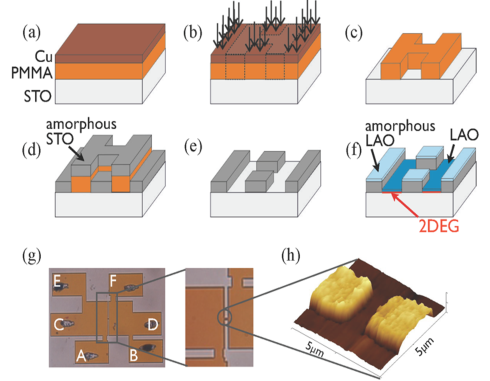
The steps for the fabrication of nanoscale bridges are illustrated in Figure 1. The process avoids an ion milling step, which could damage the STO crystal with, for instance, the creation of oxygen vacancies. henrich A template with the desired pattern is realized on the substrates by depositing an amorphous STO layer before the epitaxial growth of the LAO thin film. To this purpose, we pattern a resist mask on the bare STO substrate (Figures 1(a), (b) and (c)) using an electron beam lithography procedure optimized for insulating materials. Specifically, prior to exposure, we cover the PMMA resist with a thin film of copper (7 nm, see Figure 1(a))PMMA . This metallic film acts as a charge dispersion layer, reducing accumulation of surface charges on the STO insulating substrate. It has a minimal influence on the pattern resolution, while increases slightly the exposure dose required for PMMA.Cu_overlayer After exposure, the copper layer is removed by wet etching using a solution of FeCl in water, then the PMMA is developed using a diluted methyl isobutyl ketone (MIBK) solution, revealing the pattern. After development, we deposit a thin layer (15 nm) of amorphous STO (Figure 1(d)), before removing the resist with a lift-off procedure. Thus we obtain a template substrate with the desired pattern made of an amorphous STO layer (Figure 1(e)).banerjee Finally, an epitaxial 10 u.c.-thick LAO film is deposited using pulsed laser deposition (Figure 1(f)).cancellieri The film is grown at 800∘C in 10-4 mbar of oxygen. The KrF excimer laser fluency is 0.6 J/cm2 with a repetition rate of 1 Hz. Immediately after deposition, the sample is annealed in oxygen: we fill the deposition chamber with 200 mbar of oxygen and keep the sample temperature at 520∘C for 1 hour. The sample is then slowly cooled down to room temperature in the same oxygen atmosphere.aSTO The growth process is monitored in situ using reflection high energy electron diffraction (RHEED), which shows, for all the samples, a layer-by-layer growth mode. An atomic force microscope image of an 800 nm-wide and 2 m-long bridge realized with this technique is shown in Fig. 1(h).
We have fabricated several tens of bridges of different width, with good reproducibility of the transport parameters. Using the layout shown in Fig. 1(g), we are able to measure the properties of both the bridges and of the larger area adjoining each of them, using a four-point DC technique. We inject current through contacts C-D and measure the voltage drop between A and F to probe the bridges, and between B and F (or A and E) to probe the larger areas.
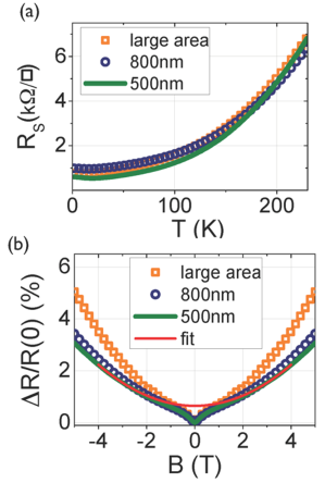
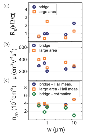
Figure 2(a) shows the metallic behavior of two devices, 500 nm (green line) and 800 nm (blue circles) wide, both 2 m-long, and of a large area of dimensions 300 m300 m (orange squares). Figure 3(a) summarizes the sheet resistance values measured at 1.5 K for devices of different size realized on the same chip and for the large areas adjoining each of them. Figure 2(b) displays the magnetoresistance of the same devices, measured at 1.5 K. Fitting the quadratic behavior of the magnetoresistance with the relation pearson ; kuchar (see for example the fit referring to the 500 nm bridge in Figure 2(b)), we estimate the mobility of the charge carriers for channels of different width as well as for the large areas. These data are plotted in Figure 3(b). From these measurements, we can also estimate the number of carriers in the bridge ( is the electron charge). As shown in Figure 3(c), (green diamonds), a typical value for LAO/STO interfaces. The analysis of the Hall data measured directly across the bridge and in the large areas yields comparable carrier densities, as can be observed in the same Figure. We observe that the values shown in Figure 3 change by a factor of 3 for channel widths spanning almost two orders of magnitude from 500 nm to 10 m,afm as well as for the large areas of different devices. Fluctuations of this amplitude in the sheet resistance and mobility are fully compatible with variations observed from sample to sample, as reported in the literature by different groups for the same growth conditions. These results allow us to affirm that processing and confinement down to the sub-micron scale do not alter the carrier population and the transport properties, which appear to be homogeneous in the different areas of the sample.
When cooled to millikevin temperatures, these devices exhibit superconducting behavior. We measured voltage vs. current () characteristics at T=40 mK in a dilution refrigerator equipped with copper powder filters, using a four terminal configuration. Figure 4(a) and (b) show plots of the 500 nm and 800 nm wide devices revealing a superconducting state for these LAO/STO structures in the sub-micron range. The critical current densities are 150 and 430 A/cm for the 500 nm, 800 nm bridges respectively. These values are in line with a previous workreyren_science07 where large-scale devices were measured. Their scatter is of the same order of that observed in transport parameters in the normal state (see Figure 3). The critical current can be tuned applying a gate voltage. Figure 4 shows the modulation of the characteristics for the 500 nm and 800 nm devices obtained in a back-gate configuration.caviglia_nature08 We observe that a complete suppression of the critical current occurs for Vg=-100 V for the 500 nm device (panel (a)). For the 800 nm device, the zero resistance state is lost only below Vg=-160 V (panel b).
In the normal state, the confinement of the 2DEG allows us to access the mesoscopic transport regime which, for phase coherent transport, manifests itself with the appearance of universal conductance fluctuations.lee_stone_PRB87 ; beenakker_review UCF stem from quantum interference of phase-coherent electron waves scattered by impurities in a sample with dimensions comparable to the phase coherence length . For the amplitude of such fluctuations is expected to have the universal value . Estimations of in LAO/STO interfaces yield values in the range of 100-200 nm at 1.5 K. caviglia_prlso ; dagan_PRB10 ; dikin_PRL11 Therefore our small bridges are expected to display UCF at low temperatures, albeit with a reduced amplitude since their dimensions are still larger than .
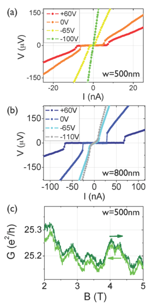
Figure 4(c) shows a magnetoconductance trace of the 500 nm wide device measured at 40 mK. The aperiodic fluctuations which can be seen have all the fingerprints of UCF. The two traces shown in the plot refer to the two sweep directions of the magnetic field, demonstrating the reproducibility of the fluctuation pattern. The phase-coherence length can be calculated from the typical average magnetic field spacing of the fluctuations via the equation:lee_stone_PRB87 ; beenakker_review , where is the quantum of flux and is a constant of the order of unity.DBc This estimation leads to 110 nm. If we now consider the amplitude of the fluctuations, we observe that it is reduced with respect to the universal value. For the curve shown in Figure 4(c) it amounts to about 8 of . A reduction in the amplitude is indeed expected when the mesoscopic channel has dimensions larger than . In this case, the channel may be subdivided into coherent areas of dimensions ; the conductance fluctuations of each of these areas will be of order and all the areas in the channel will add incoherently, leading to classical self-averaging. The resulting conductance fluctuations will be reduced by a factor proportional to , with and the width and length of the bridge respectively.lee_stone_PRB87 Considering our geometry, our results are in good numerical agreement with this argument.
In summary, we reported a detailed study of nanodevices based on the 2DEG at the LAO/STO interface.
Mesoscopic bridges with widths down
to 500 nm were realized using electron beam lithography.
Possible damage to the STO substrate, such as oxygen losses,
were avoided by resorting to an amorphous STO template.
The detailed transport characterization reveals that processing
and confinement down to the sub-micron scale do not alter substantially the
carrier profile and that the samples are homogeneous down to the scale of our
smallest bridges. The confinement of the 2DEG in the in-plane direction results in universal
conductance fluctuations that were observed in magnetotransport at low
temperatures. The devices show superconducting behavior, with a critical
current tunable using field effect. The observation of a zero-resistance state in LAO/STO
nanodevices opens exciting perspectives for the study of quasi-one dimensional
superconductivity and for the realization of devices such as tunable Josephson
junctions.
We thank P.Zubko for careful reading of the manuscript and M. Lopes and S. C. Müller for their technical
assistance. This work was supported
by the Swiss National Science Foundation through the National Center of
Competence in Research, Materials
with Novel Electronic Properties, MaNEP, division II, and the European Union
through the project OxIDes.
References
- (1) A. Ohtomo and H. Y. Hwang, Nature (London) 427, 423 (2004).
- (2) J. Mannhart and D. G. Schlom, Science 327, 1607 (2010).
- (3) P. Zubko, S. Gariglio, M. Gabay, P. Ghosez, and J.-M. Triscone, Ann. Rev. Cond. Matter Phys. 2, 141 (2011).
- (4) N. Reyren, S. Thiel, A. D. Caviglia, L. Fitting Kourkoutis, G. Hammerl, C. Richter, C. W. Schneider, T. Kopp, A.-S. Ruetschi, D. Jaccard, M. Gabay, D. A. Muller, J.-M. Triscone, and J. Mannhart, Science 317, 1196 (2007).
- (5) A. D. Caviglia, S. Gariglio, N. Reyren, D. Jaccard, T. Schneider, M. Gabay, S. Thiel, G. Hammerl, J. Mannhart, and J.-M. Triscone, Nature 456, 624 (2008).
- (6) C. Bell, S. Harashima, Y. Kozuka, M. Kim, B. G. Kim, Y. Hikita, and H. Y. Hwang, Phys. Rev. Lett. 103, 226802 (2009).
- (7) A. D. Caviglia, M. Gabay, S. Gariglio, N. Reyren, C. Cancellieri, and J. M. Triscone, Phys. Rev. Lett. 104, 126803 (2010).
- (8) M. Ben Shalom, M. Sachs, D. Rakhmilevitch, A. Palevski, and Y. Dagan, Phys. Rev. Lett. 104, 126802 (2010).
- (9) M. Basletic, J. Maurice, C. Carrtro, G. Herranz, O. Copie, M. Bibes, E. Jacquet, K. Bouzehouane, S. Fusil, and A. Barthlmy, Nature Mater. 7, 621 (2008).
- (10) N. Reyren, S. Gariglio, A. D. Caviglia, D. Jaccard, T. Schneider, and J.-M. Triscone, Appl. Phys. Lett. 94, 112506 (2009).
- (11) A. D. Caviglia, S. Gariglio, C. Cancellieri, B. Sacp, A. Fte, N. Reyren, M. Gabay, A. F. Morpurgo, and J. M. Triscone, Phys. Rev. Lett. 105, 236802 (2010).
- (12) M. Ben Shalom, A. Ron, A. Palevski, and Y. Dagan, Phys. Rev. Lett. 105, 206401 (2010)
- (13) S. Gariglio, M. Gabay, and J.-M. Triscone, Nature Nano. 5, 13 (2010).
- (14) R. P. Kaur, D. F. Agterberg, and M. Sigrist, Phys. Rev. Lett. 94, 137002 (2005).
- (15) B. Liu and X. Hu, Phys. Rev. B 81, 144504 (2010).
- (16) C. Cen, S. Thiel, G. Hammerl, C. W. Schneider, K. E. Andersen, C. S. Hellberg, J. Mannhart, and J. Levy, Nat. Mat. 7, 298 (2008).
- (17) C. Cen, S. Thiel, J. Mannhart, and J. Levy, Science 323, 1026 (2009).
- (18) Y. Xie, C. Bell, T. Yajima, Y. Hikita, and H. Y. Hwang, Nano Lett. 10, 2588 (2010).
- (19) C. W. Schneider, S. Thiel, G. Hammerl, C. Richter, and J. Mannhart, Appl. Phys. Lett. 89, 12210 (2006).
- (20) D. Rakhmilevitch, M. Ben Shalom, M. Eshkol, A. Tsukernik, A. Palevski, and Y. Dagan, Phys. Rev. B 82, 235119 (2010).
- (21) V.E. Henrich, G. Dresselhaus, and H.J. Zeiger, Phys. Rev. B 17, 4908 (1978).
- (22) We used two layers of PMMA, with 495 K and 950 K molecular weight, both with a 3 solid content in anisole, for a total thickness of 300nm. The double layer was used in order to facilitate the subsequent lift-off step.
- (23) C. B. Samantaray and J. T. Hastings, J. Vac. Sci. Technol. B 26, 2300 (2008)
- (24) A similar template approach has been reported recently by N. Banerjee, M. Huijben, G. Koster, and G. Rijnders, Appl. Phys. Lett. 100, 041601 (2012).
- (25) C. Cancellieri, N. Reyren, S. Gariglio, A. D. Caviglia, A. Fte, and J.-M. Triscone, Europhys. Lett. 91, 17004 (2010).
- (26) At the end of our fabrication process, the interface between the STO substrate and the amorphous STO layer is observed to be insulating.
- (27) G. Pearson and H. Suhl, Phys. Rev. 83, 768 (1951).
- (28) F. Kuchar and P. Frankus, Phys. Rev. B 16, 874 (1977).
- (29) The lateral dimension of each bridge is confirmed using AFM topography.
- (30) P. A. Lee, A. Stone, and H. Fukuyama, Phys. Rev. B 35, 1039 (1987).
- (31) C. W. J. Beenakker and H. van Houten, Solid State Physics 44, 1 (1991).
- (32) D. A. Dikin, M. Mehta, C. W. Bark, C. M. Folkman, C. B. Eom, and V. Chandrasekhar, Phys. Rev. Lett. 107, 056802 (2011).
- (33) An exact estimation of the correlation field is given by the full width at half maximum of the magneto conductance autocorrelation function, which fully captures the characteristic length scales of a mesoscopic system.