Multiple time scale blinking in InAs quantum dot single-photon sources
Abstract
We use photon correlation measurements to study blinking in single, epitaxially-grown self-assembled InAs quantum dots situated in circular Bragg grating and microdisk cavities. The normalized second-order correlation function is studied across eleven orders of magnitude in time, and shows signatures of blinking over timescales ranging from tens of nanoseconds to tens of milliseconds. The data is fit to a multi-level system rate equation model that includes multiple non-radiating (dark) states, from which radiative quantum yields significantly less than 1 are obtained. This behavior is observed even in situations for which a direct histogramming analysis of the emission time-trace data produces inconclusive results.
pacs:
78.55.Cr,81.07.Ta,85.35.Be,78.67.HcSingle-photon sources based on single epitaxially-grown quantum dots (QDs) are promising devices for photonic quantum information scienceMichler (2003); O’Brien et al. (2009). As single-photon source brightness is crucial in many applications, III-V compound nanostructures like InAs QDs in GaAs are of particular interest, both due to their short radiative lifetimes (typically nsDalgarno et al. (2008)) and the availability of mature device fabrication technology for creating scalable nanophotonic structures which can modify the QD radiative properties in desirable ways. In particular, structures can be created to further increase the QD radiative rateGérard and Gayral (1999) and funnel a large fraction of the emitted photons into a desired collection channelBarnes et al. (2002).
The overall brightness of the source is, however, also influenced by the radiative efficiency of the QD, which can deviate from unity for a variety of reasons, including coupling of the radiative transition to non-fluorescing states. Such fluorescence intermittency, also called blinking, is an apparently ubiquitous phenomenon in solid-state quantum emittersNirmal et al. (1996); Kuno et al. (2000); Stefani et al. (2009); Frantsuzov et al. (2008), being particularly pronounced in single nanocrystal QDs and organic molecules. In contrast, blinking in epitaxially-grown III-V QDs has not received as much attention, largely due to the fact that such QDs, grown in ultra-high-vacuum environments and embedded tens of nanometers below exposed surfaces, typically do not express pronounced fluorescence intermittency Lounis and Orrit (2005); Michler (2009). Obvious blinking (at the ms to s time scales) has only been observed in InGaAs QDs grown close to crystal defectsWang et al. (2005) and in some InP QDsPistol et al. (1999); Sugisaki et al. (2001). Sub-microsecond blinking dynamics in InAs QDs have also been studiedSantori et al. (2004).
Here, we study blinking in InAs/GaAs QDs embedded in photonic nanostructures that enable high collection efficiencies (10 )Davanço et al. (2011); Ates et al. (2012). As these devices do not exhibit pronounced fluorescence variations, we use photon correlation measurementsLippitz et al. (2005) as a more informative approach to investigate blinking over time scales ranging from tens of nanoseconds to hundreds of milliseconds. The data is fit with a multi-level rate equation model for the QD that yields estimates for the transition rates and occupancies of the QD states, enabling an overall estimate of the QD radiative efficiency. Notably, we find quantum yields significantly less than 1 even in QDs which show no blinking in histogramming analysis. This information is valuable in quantifying the extraction efficiency of QD emission, and in understanding the ultimate brightness achievable for QD single-photon sources. We anticipate that the importance of this topic is likely to grow as epitaxially-grown QDs are incorporated within photonic nanostructures with critical dimensions of tens of nanometers, at which point surfaces play an important roleWang et al. (2004).
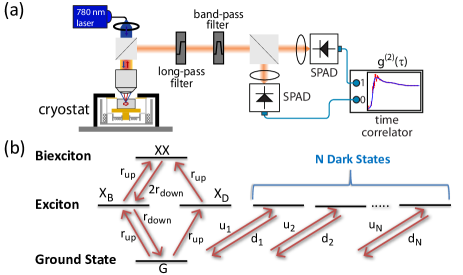
Our samples consist of InAs QDs embedded in the center of a 190 nm thick GaAs layer. The collection efficiency of emitted photons is enhanced through the use of a circular grating microcavityDavanço et al. (2011); Ates et al. (2012) or fiber-coupled microdisk cavity geometryAtes et al. (2013), as detailed in the Supplementary Materialref . The devices are cooled to 10 K in a liquid helium flow cryostat and excited by a 780 nm (above the GaAs bandgap) continuous wave laser. The collected emission is spectrally filtered (bandwidth nm eV) to select a single state of a single QD (typically the bi-exciton or neutral exciton state), split on a 50/50 beamsplitter, and sent to a pair of silicon single-photon counting avalanche diodes (SPADs) (see Fig. 1(a)). The SPAD outputs are directed to a time-correlator that records photon arrival times for each channel with a resolution of 4 ps. Data is typically recorded over a period of 1 h. Results from three different devices (labeled 1,2,3) are described below.
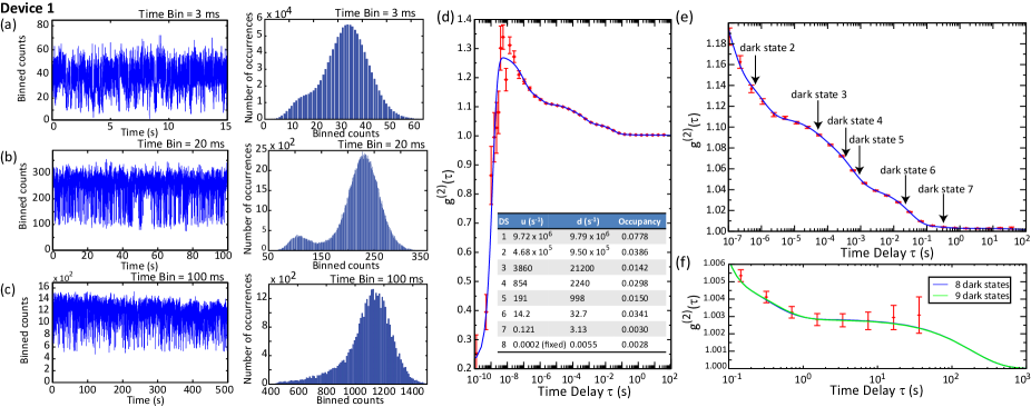
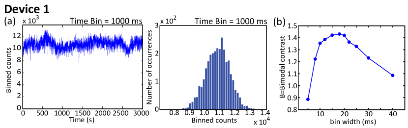
Figure 2(a) shows a portion of the fluorescence time trace recorded from device 1, where detection events are binned into 3 ms bins. The time trace data clearly shows a fluctuating fluorescence intensity, more often exhibiting high than low levels. This is further seen in the histogram of detection events per bin shown next to the time trace, which exhibits a bimodal behavior biased towards the higher count rates. Figures 2(b) and 2(c) show the corresponding time trace and histogram data for 20 ms and 100 ms time bins. At the 20 ms bin width, a bimodal distribution in the histogram is more clearly seen. At 100 ms, it becomes less visible, as is the contrast between high and low intensities in the time trace. When the bin width is increased to 1000 ms, obvious signs of blinking are no longer observable in either the time trace or histogram dataref .
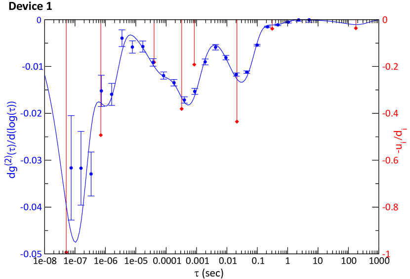
The sensitivity of time trace and histogram data to the choice of bin width is well-knownLippitz et al. (2005); Verberk and Orrit (2003); Crouch et al. (2010), and can limit the ability to achieve a complete picture of the system dynamics. In particular, the minimum reliable bin size is limited by the available photon flux and the shot noise, while too large bin sizes average out fluctuations occurring at shorter time scales. Histogram analysis of the high or low fluorescence level time interval distributions is furthermore influenced by the selection of a threshold intensity level. In contrast, intensity autocorrelation analysis does not require such potentially arbitrary input parameters. In Fig. 2(d), we plot the intensity autocorrelation function for device 1 over a time range exceeding eleven orders of magnitude (error bars are due to fluctuations in the detected photon count rates, and represent one standard deviationref ). This data, calculated using an efficient approachref similar to that described in ref. Laurence et al., 2006, indicates that the photon antibunching at =0, expected for a single-photon emitter, is followed by photon bunching that peaks in the 10 ns region before slowly decaying, with only occurring for s (see zoomed-in data in Fig. 2(e)). The decay in is punctuated by a series of inflection points (’shoulders’) in which the concavity of the curve changes. Such features have been observed in fluorescence autocorrelation curves of single aromatic molecules in polymeric hostsZumbusch et al. (1993); Fleury et al. (1993). Photon bunching in these systems arises from shelving of the molecule into dark triplet states, resulting in bursts of emitted photons followed by dark intervals at characteristic rates. Similar behavior can also originate from interactions between the molecule and neighboring two-level systems (TLS) in the host polymer. Switching between the states of the TLS leads to sudden jumps in emission frequency, and correspondingly, emission intensity. Multiple shoulders in the autocorrelation have been associated with coupling to a number of TLSs with varying switching rates.
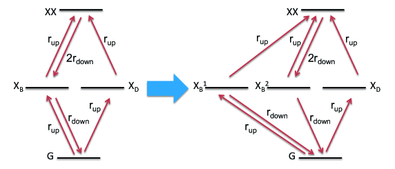
We interpret our data similarly, taking the radiative QD transition to be coupled to multiple non-radiative, or dark, statesref , as depicted in Fig. 1(b). This phenomenological model is motivated by potential physical mechanisms present in self-assembled InAs/GaAs QDs. For example, lattice defects in the vicinity of the QD can act as carrier traps, and charge tunneling events between the QD and such traps lead to fluorescence intermittencyWang et al. (2005); Pistol et al. (1999). Perturbation of the electron and hole wavefunction overlap by the local electric field of trapped charges has also been postulated as a cause of blinkingSugisaki et al. (2001). Another possibility is that tunneling of carriers into nearby traps causes spectral shifts of the QD emission out of the nm filter bandwidth, leading to an effective blinking behavior. Such shifts would however be larger than the spectral diffusion measurements recently reportedBerthelot et al. (2006); Abbarchi et al. (2012); Vamivakas et al. (2011); Houel et al. (2012). We did not observe such spectral diffusion in spectroscopy with a 0.035 nm resolution.
In these scenarios, interactions with surrounding traps drive the QD into high or low emission states with well-defined rates, consistent with the model of Fig. 1(b). Here, each dark state is populated at a rate and de-populated at a rate . We solve the rate equations to compute using the appropriate transition for each device: The XX XB transition for devices 1 and 2, and the XB G transition for device 3. All parameters are varied in the fit except for the radiative decay rate, , which is determined from independent measurementsref . A first estimate of the number of dark states used in the model is the number of shoulders in the measured data. Ultimately, the number of dark states is determined by the parameter minimized in the fit, as defined inref .
Fits to device 1 data are shown as blue solid lines in Figs. 2(d)-(e), along with extracted occupancy and population and de-population rates, and , of each dark state. The short ( ns) time behavior of depends primarily on the excitation rate , the decay rate , the SPAD timing jitter, and the background signal, if presentref . The behavior at longer times depends primarily on and . Accurate fits require a minimum number of dark states (8 for this device), below which the behavior of , quantified by the fit , is not well reproduced. Larger has negligible impact on the fit (Fig. 2(f)), and the total dark state occupancy changes by . The radiative quantum yield (radiative efficiency) is estimated by subtracting this total dark state occupancy from unity. We note that as the rates coupling states G, XB, XD, and XX are more than an order of magnitude faster than rates to the dark states, the quality of the fits and the resulting quantum yield does not depend on whether the dark states are coupled to G (Fig. 1) or XB. Similarly, replacing the dark states with partially emissive gray statesSpinicelli et al. (2009), modeled with a branching ratio between dark and bright transitions, does not significantly affect the fits or computed quantum yieldref .
In all, the data and rate equation analysis uncover qualitatively new information about blinking in this device in comparison to the time trace and histogram data. First, we see that blinking occurs across a wide variety of time scales. While blinking at sub-microsecond time scales has been reported in epitaxially grown InAs QDs previouslySantori et al. (2004); Volz et al. (2012), our measurements show that these systems can exhibit blinking out to hundreds of milliseconds. One physical picture qualitatively consistent with this observation would be that blinking is caused by the tunneling of carriers between the QD and several adjacent traps of varying separation from the QD. For example, Sercel and colleagues have considered electron relaxation from a QD through a deep level trap Sercel (1995); Schroeter et al. (1996), and calculated that tunneling rates can vary by several orders of magnitude over a few tens of nanometers of QD-trap separation (see Supplementary Material for a plot of these tunneling rates). Such deep level traps may arise during the QD growth process itself Sercel (1995); Lin et al. (2005); Asano et al. (2010) may physically correspond to impurities, such as vacancies, antisites, and interstitials, produced during growth and post-growth fabrication processes. We point out that a rapid thermal annealing step was used to blue-shift the QD emission in our wafers ref ; Lin et al. (2006), prior to device fabrication.
The estimated total dark state occupancy is , so the radiative transition is still dominantly preferred over excitation into the dark states, with a radiative quantum yield of . Finally, we note that the rates and for populating/de-populating dark state can at least be qualitatively linked to the location of prominent features in the data. For example, in a system consisting of a single dark state that is populated and de-populated at rates and , the slope of plotted vs. is maximimal at Lippitz et al. (2005). In a system comprised of multiple dark states, if excitation and decay rates are sufficiently different, the values still approximately point to slope maxima. Figure 2(e) identifies these points, which qualitatively match the experimentally observed maximum slope points. Quantitative details are given inref .
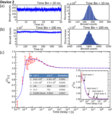
Repeating this analysis for device 2 yields the results in Fig. 3. Here, neither time trace nor histogram data show clear evidence of blinking. In contrast, in Fig. 3(c) again evidences bunching at the ten nanosecond time scale, followed by a series of shoulders, before reaching a value of unity. The data is fit to a rate equation model with five dark states, and again shows close correspondence (inset to Fig. 3(c)). Contrasting with device 1, blinking at longer times (e.g., s) is significantly less pronounced, and the estimated total dark state occupancy is .
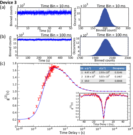
Finally, we present data from device 3 in Fig. 4. Similar to device 2, the time trace and histogram data show little evidence of blinking. The data does reveal significant blinking over sub-microsecond time scales, but at longer times blinking is minimal and the system can be well fit to a model with (with final state occupancy ). Interestingly, the total dark state occupancy is , significantly greater than observed in either device 1 or 2. Thus, despite qualitative similarity with the time trace and histogram data of device 2, the dynamics of the QD are in fact qualitatively different, as revealed by the photon correlation measurements. This qualitative difference is perhaps unsurprising given its entirely different device history (different wafer growth; no rapid thermal annealing ref . Also, as the pronounced bunching persists out to s time scales, an accurate estimate of , needed for assessing the purity of the single-photon source, requires acquisition and analysis of data out to many orders of magnitude longer times than the characteristic time scale of the antibunching dip.
Correlation functions can reveal the kinetics of the blinking signal over a large time range, however only in a time-averaged senseLippitz et al. (2005). Information about instantaneous intensity fluctuations, such as probability distributions for bright and dark intervals, can be obtained from photon-counting histograms, as commonly done in the blinking literatureLippitz et al. (2005); Stefani et al. (2009); Crouch et al. (2010). Applied to epitaxially-grown QDs, this type of analysis has revealed exponential blinking time distributionsPistol et al. (1999); Sugisaki et al. (2001); Wang et al. (2005), suggesting modification of the QD fluorescence by one or a few neighboring centers, as discussed (nanocrystal QDs have in contrast been shown to display power-law distributionsCrouch et al. (2010)). We have applied this technique to the QD in Device 1. Although our measured data does not strictly follow the stringent criteria suggested inCrouch et al. (2010) for reliable parameter extraction, we see strong indications of exponential probability distributionsref .
In summary, photon correlation measurements taken over eleven orders of magnitude in time are used to study blinking in epitaxially-grown, self-assembled InAs QDs housed in photonic nanocavities. The measurements are fitted to a rate equation model consisting of a radiative transition coupled to a number of dark states. The model reproduces the observed behavior, allowing us to quantify the multiple blinking time scales present and estimate the QD radiative efficiency, which ranges between 53 and 85. We anticipate that this approach will be valuable in studying the behavior of InAs QDs in proximity ( nm) to etched surfaces and/or metals in nanophotonic/nanoplasmonic geometries. Indeed, the blinking observed here may stem from traps produced in the fabrication of the nanostructures used to enhance QD emission collection. Measuring photon correlations across this broad range of time scales both before and after nanofabrication may help elucidate the origin of blinking in these systems.
C.S.H. acknowledges the CNST Visiting Fellow program and support from the Office of Naval Research through the Naval Research Laboratory’s Basic Research Program. M.D. and S.A. acknowledge support under the Cooperative Research Agreement between the University of Maryland and NIST-CNST, Award 70NANB10H193.
References
- Michler (2003) P. Michler, ed., Single Quantum Dots (Springer Verlag, Berlin, 2003).
- O’Brien et al. (2009) J. L. O’Brien, A. Furusawa, and J. Vučković, Nature Photonics 3, 687 (2009).
- Dalgarno et al. (2008) P. A. Dalgarno, J. M. Smith, J. McFarlane, B. D. Gerardot, K. Karrai, A. Badolato, P. M. Petroff, and R. J. Warburton, Phys. Rev. B 77, 245311 (2008).
- Gérard and Gayral (1999) J.-M. Gérard and B. Gayral, J. Lightwave Tech. 17, 2089 (1999).
- Barnes et al. (2002) W. L. Barnes, G. Bjrk, J. Gérard, P. Jonsson, J. A. E. Wasey, P. T. Worthing, and V. Zwiller, Eur. Phys. J. D 18, 197 (2002).
- Nirmal et al. (1996) M. Nirmal, B. O. Dabbousi, M. G. Bawendi, J. J. Macklin, J. K. Trautman, T. D. Harris, and L. E. Brus, Nature 383, 802 (1996).
- Kuno et al. (2000) M. Kuno, D. P. Fromm, H. F. Hamann, A. Gallagher, and D. J. Nesbitt, J. Chem. Phys. 112, 3117 (2000).
- Stefani et al. (2009) F. D. Stefani, J. P. Hoogenboom, and E. Barkai, Physics Today 62, 34 (2009).
- Frantsuzov et al. (2008) P. Frantsuzov, M. Kuno, B. Janko, and R. A. Marcus, Nature Physics 4, 519 (2008).
- Lounis and Orrit (2005) B. Lounis and M. Orrit, Reports on Progress in Physics 68, 1129 (2005).
- Michler (2009) P. Michler, ed., Single Semiconductor Quantum Dots (Springer Verlag, Berlin, 2009).
- Wang et al. (2005) X. Y. Wang, W. Q. Ma, J. Y. Zhang, G. J. Salamo, M. Xiao, and C. K. Shih, Nano Letters 5, 1873 (2005).
- Pistol et al. (1999) M.-E. Pistol, P. Castrillo, D. Hessman, J. A. Prieto, and L. Samuelson, Phys. Rev. B 59, 10725 (1999).
- Sugisaki et al. (2001) M. Sugisaki, H.-W. Ren, K. Nishi, and Y. Masumoto, Phys. Rev. Lett. 86, 4883 (2001).
- Santori et al. (2004) C. Santori, D. Fattal, J. Vuckovic, G. S. Solomon, E. Waks, and Y. Yamamoto, Phys. Rev. B 69, 205324 (2004).
- Davanço et al. (2011) M. Davanço, M. T. Rakher, D. Schuh, A. Badolato, and K. Srinivasan, Appl. Phys. Lett. 99, 041102 (2011).
- Ates et al. (2012) S. Ates, L. Sapienza, M. Davanço, A. Badolato, and K. Srinivasan, IEEE J. Sel. Top. Quan. Elec. 18, 1711 (2012).
- Lippitz et al. (2005) M. Lippitz, F. Kulzer, and M. Orrit, ChemPhysChem 6, 770 (2005).
- Wang et al. (2004) C. F. Wang, A. Badolato, I. Wilson-Rae, P. M. Petroff, E. Hu, J. Urayama, and A. Imamoglu, Appl. Phys. Lett. 85, 3423 (2004).
- Ates et al. (2013) S. Ates, I. Agha, A. Gulinatti, I. Rech, A. Badolato, and K. Srinivasan, Scientific Reports 3, 1397 (2013).
- (21) See supplementary material for details regarding the device fabrication, fluorescence spectra, calculation of from the measured time tagged data, the rate equation model used to fit the experimental data, labeling of the dark states, and on/off time distribution data.
- Verberk and Orrit (2003) R. Verberk and M. Orrit, J. Chem. Phys. 119, 2214 (2003).
- Crouch et al. (2010) C. H. Crouch, O. Sauter, X. Wu, R. Purcell, C. Querner, M. Drndic, and M. Pelton, Nano Letters 10, 1692 (2010).
- Laurence et al. (2006) T. A. Laurence, S. Fore, and T. Huser, Opt. Lett. 31, 829 (2006).
- Zumbusch et al. (1993) A. Zumbusch, L. Fleury, R. Brown, J. Bernard, and M. Orrit, Phys. Rev. Lett. 70, 3584 (1993).
- Fleury et al. (1993) L. Fleury, A. Zumbusch, M. Orrit, R. Brown, and J. Bernard, Journal of Luminescence 56, 15 (1993).
- Berthelot et al. (2006) A. Berthelot, I. Favero, G. Cassabois, C. Voisin, C. Delalande, P. Roussignol, R. Ferreira, and J. M. Gérard, Nature Physics 2, 759 (2006).
- Abbarchi et al. (2012) M. Abbarchi, T. Kuroda, T. Mano, M. Gurioli, and K. Sakoda, Phys. Rev. B 86, 115330 (2012).
- Vamivakas et al. (2011) A. N. Vamivakas, Y. Zhao, S. Fält, A. Badolato, J. M. Taylor, and M. Atatüre, Phys. Rev. Lett. 107, 166802 (2011).
- Houel et al. (2012) J. Houel, A. V. Kuhlmann, L. Greuter, F. Xue, M. Poggio, R. J. Warburton, B. D. Gerardot, P. A. Dalgarno, A. Badolato, P. M. Petroff, A. Ludwig, D. Reuter, and A. D. Wieck, Phys. Rev. Lett. 108, 107401 (2012).
- Spinicelli et al. (2009) P. Spinicelli, S. Buil, X. Quélin, B. Mahler, B. Dubertret, and J.-P. Hermier, Phys. Rev. Lett. 102, 136801 (2009).
- Volz et al. (2012) T. Volz, A. Reinhard, M. Winger, A. Badolato, K. J. Hennessy, E. L. Hu, and A. Imamoğlu, Nature Photonics 6, 607 (2012).
- Sercel (1995) P. C. Sercel, Phys. Rev. B 51, 14532 (1995).
- Schroeter et al. (1996) D. F. Schroeter, D. J. Griffiths, and P. C. Sercel, Phys. Rev. B 54, 1486 (1996).
- Lin et al. (2005) S. W. Lin, C. Balocco, M. Missous, A. R. Peaker, and A. M. Song, Phys. Rev. B 72, 165302 (2005).
- Asano et al. (2010) T. Asano, Z. Fang, and A. Madhukar, J. Appl. Phys. 107, 073111 (2010).
- Lin et al. (2006) S. W. Lin, A. M. Song, N. Rigopolis, B. Hamilton, A. R. Peaker, and M. Missous, J. Appl. Phys. 100, 043703 (2006).
Supplementary Material for
Multiple time scale blinking in InAs quantum dot single-photon sources
Marcelo Davanço C. Stephen Hellberg Serkan Ates Antonio Badolato Kartik Srinivasan
I Supplemental Information
II Device Details
Devices based on two different quantum dot (QD) wafers are studied in this work. Devices 1 and 2 come from wafer A, which is made of an epistructure consisting of a 190 nm thick GaAs waveguide layer on top of a 1 m thick, Al0.6Ga0.4As sacrificial layer. The as-grown emission wavelength of the QD s-shell is near 1100 nm, so the samples are blue-shifted to a wavelength near 940 nm using a rapid thermal annealing process Malik et al. (1997) performed at 830∘C, so that the QD emission can be detected using efficient Si single-photon avalanche diodes (SPADs). Circular grating microcavities Davanço et al. (2011); Ates et al. (2012) are fabricated in order to increase the fraction of QD emission collected by the 0.42 numerical aperture (NA) lens used in the confocal microscope setup.
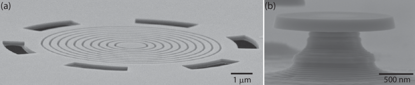
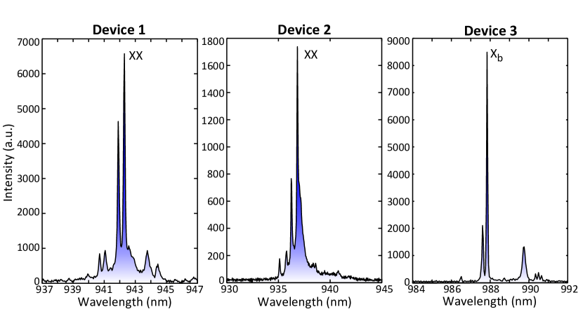
Device 3 comes from wafer B, which is made of a similar epistructure as wafer A, but has an as-grown QD s-shell emission wavelength near 980 nm, so that no rapid thermal annealing process is performed on this wafer (in comparison to Devices 1 and 2, we note that the lack of a rapid thermal annealing step may have a significant effect on the behavior of deep level traps in the material Lin et al. (2006)). Microdisk cavities are fabricated to increase the collection efficiency of emitted photons, with a fiber taper waveguide interface used to extract photons from the microdisk optical mode Ates et al. (2013). Scanning electron microscope images of the fabricated devices are shown in Fig. S1. Figure S2 shows the fluorescence spectrum of each device, under the non-resonant 780 nm cw excitation conditions used in the photon counting measurements presented in the main text.
Devices 1 and 2 were previously studied under pulsed (80 MHz rep rate), 820 nm non-resonant excitation in Ref. Ates et al. (2012), where the performance of the devices as triggered single-photon sources was assessed. There, a photon collection efficiency of 9.5 and 5.6 into the NA=0.42 lens was estimated for the two devices, respectively, under the assumption of unity radiative quantum yield. As the radiative quantum yields we estimate in the main text of the current work are less than unity (78 and 86 ), this indicates that the collection efficiencies determined in the prior work were likely underestimated (by approximately 28 and 16 , respectively). This correction is tentatively presented, however, both because the data for the two works were acquired on different occasions, and more importantly, because the excitation conditions differ (different wavelength and pulsed vs. cw pumping). Finally, we note that while Device 3 comes from the same chip as the fiber-coupled microdisk single-photon source studied in Ref. Ates et al. (2013), it is not precisely the same device, and had an estimated collection efficiency that was about an order of magnitude lower (on the order of 1 into one channel of the optical fiber).
III Experimental details
The devices were cooled to 10 K in a liquid helium flow cryostat and excited, non-resonantly, by a 780 nm (above the GaAs bandgap) continuous wave laser. Devices 1 and 2 were excited with a free-space beam though a NA 0.42 objective. Photoluminescence (PL) emitted by QDs contained in the circular grating microcavities was collected through the same objective and focused into a single-mode optical fiber, to be routed towards detection Ates et al. (2012). Quantum dots in Device 3 were optically excited with a fiber taper waveguide (FTW) evanescently coupled to the hosting microdisk, and the emitted PL was collected with the same optical fiber Ates et al. (2013). In both situations, the collected PL was spectrally filtered to select only a single state of a single QD (the bi-exciton or neutral exciton state - see Fig. S2). For devices 1 and 2, a monochromator was used as a filter, with a bandwidth of pm. In the case of Device 3, two cascaded holographic gratings were used, providing an overall bandwidth of pm. The filtered PL was split on a 50/50 beamsplitter and sent to a pair of silicon single-photon counting avalanche diodes (SPADs). The SPAD outputs were directed to a time-correlator that recorded photon arrival times for each channel with a resolution of 4 ps. The SPAD timing jitter was ps.
IV Histogram data
The measured data consisted of a series of time tags corresponding to single-photon detection events. To produce the time-domain blinking trajectories shown in the main text, detection events in the raw time-tag data were placed into a sequence of bins of duration . Histograms for number of detection events per bin were generated from the blinking trajectories. The number of histogram bins was selected through the Freedman-Diaconis method Freedman and Diaconis (1981).
In Fig. 2 in the main text, we show time trajectory and histogram data for Device 1 using time bin widths of 3 ms, 20 ms, and 100 ms. This represents essentially the full range of bin widths over which appreciable blinking can be directly observed in trajectory and histogram data. For example, a bin width of 1000 ms shows little variation in the collected emission intensity in the time trajectory, and the histogram data does not show evidence of a bimodal distribution (Fig. S3(a)).
For time bin widths over which a bimodal distribution is visible, we define a contrast parameter , where and are the intensities of the two maxima and is the minimum intensity between the two peaks. In Fig. S3(b), we plot as a function of time bin width for Device 1. We see that there is a relatively small range of time bin widths over which a bimodal distribution is evident, with the contrast optimized at ms, for which data was plotted in the main text in Fig. 2(b).
V Calculation of from time-tagged data
The experimental setup yields two streams of data corresponding to photon arrival events on SPADs 1 and 2, collected over a period of 1 h. These two data streams were used to calculate the second-order correlation function
| (S1) |
where and are the photon fluxes in SPADs 1 and 2. To calculate , we use an efficient approach similar to that in Ref. Laurence et al., 2006. We initially specify non-overlapping time windows , with , which are used to bin detection events in the SPAD 1 stream. The arrival times of all the photons in each of the M time windows is initially stored. When the time is shifted to the next arrival time in the SPAD 2 stream, photon numbers in all time windows in the SPAD 1 stream are updated, shifting on average 1 photon from window to window . Thus the overall computation scales as for photons and time windows instead of the cost of a direct computation of .
To determine the uncertainty of the calculated due to signal fluctuations caused by varying experimental conditions, the original data is divided into bins, to which the procedure above is applied. The covariance matrix
| (S2) |
is then calculated, where is the measured value of the th time window of in the th statistical bin, and is the mean over the statistical bins (we drop the (2) superscript in for clarity). The error bars shown in the plots in the main text are the standard deviations of the individual observations: .
VI Rate equation model and fits
The dynamics of the quantum dots are modeled by the transitions shown
schematically in Fig. 1b of the main text. The states are defined as:
Ground state
Bright exciton
Dark exciton
Bi-exciton
The -th dark state
The populations evolve according to the rate equations:
| (S3) | |||||
where and are the up-transition and down-transition rates between the ground state G and the th dark state. The state in the model corresponds to an electron-hole pair with parallel spins. This state, normally called the dark exciton, is approximately degenerate with the bright exciton state , however is not optically active. The additional dark states can either be non-emissive or may emit outside the filtered detection window, as detailed in the experimental setup description.
By monitoring the power dependence of the luminescence, we determined that the XX XB transition was being measured in Devices 1 and 2, while the XB G transition was measured in Device 3. For Devices 1 and 2, the correlation function is the probability that two photons from the XX XB transition are emitted a time interval apart. To compute , we integrate the rate equations (S3) setting the initial conditions to be with all other populations zero; corresponds to the probability that the system will return to state XB through the XX XB transition Carmichael and Walls (1976). To compute this probability, we split the state XB into two states in the rate equations as shown in Fig. S4. X can only be reached via the XX XB transition. All other transitions to state XB are directed to X. All transitions away from state XB are included for both X and X. Initially we set with all other populations zero. Then .
For Device 3, is the probability that two photons from the XB G transition are emitted a time interval apart. Similarly to the case above, we split state G into two states: G2 which can only be reached via the XB G2 transition, and G1, which is reached by all other transitions to G, namely the recoveries from the dark states in Fig. 1(b). Setting with all other populations zero, .
We find the short-time behavior of can be used to determine the ratio but not the individual values of and . We therefore determine the values of using independent decay-rate measurements. The values of and for the three devices are given in Table 1.
| Device | ||
|---|---|---|
| 1 | ||
| 2 | ||
| 3 |
The remaining parameters were determined by a fit of computed from the rate equations. For uncorrelated output, the covariance matrix is diagonal. With correlations, is defined as:
| (S4) |
where is the fitting function determined by solving the rate equations (S3) Hellberg and Manousakis (2000).
The fits found a background signal of 9 % for Device 3; zero background was found for Devices 1 and 2 Molski et al. (2000). A timing jitter of 450 ps was used for all devices.
VII Coupling of the dark states to the radiative transition
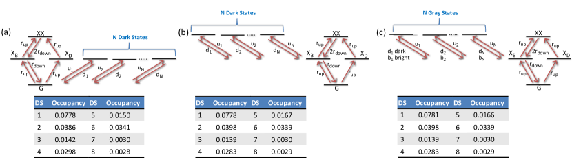
The model employed throughout this paper has the dark states coupled to the ground state G of the radiative transition (Fig. 1(b) in the main text). One might instead envision scenarios in which the dark states are coupled to other states within the radiative transition. We find that the fits are relatively insensitive to which specific state within the radiative transition they are coupled to. Physically, this is because the rates coupling the states G, XB, XD, and XX are more than an order of magnitude faster than rates to the dark states.
As an example, we compare the dark state occupancies determined based on fits to the model presented in the main text (and re-displayed in Fig. S5(a)) with occupancies based on fits to a model in which the dark states are coupled to state XB (Fig. S5(b)). Optimizing the fits based on the parameter, we find that the individual dark state occupancies and the total occupancy of the dark states (and hence, the radiative efficiency of the quantum dot) are only slightly different in the two cases.
We also considered the possibility of partially emissive ’gray’ states instead of dark states Spinicelli et al. (2009). In this model, dark state decays radiatively with rate (into the same spectral channel as the QD excitonic transition) and non-radiatively with rate , as shown schematically in Fig. S5(c). We set the radiative fraction of each dark state to be equal, so . Even with a radiative fraction as large as , the quality of the fit and the occupancies of each dark (shown in Fig. S5(c)) are nearly identical to the case with non-emitting dark states, again a consequence of the vast difference in the rates that couple the excitonic transition relative to the rates that couple to the dark states.
VIII Labeling of dark states
In the main text, we have labeled dark states in the data according to times , under the assumption that these times correspond to points of maximal slope. This assignment is expected to be only approximate, since it essentially assumes that the different dark states have no influence on each other. We compare the labeled in the above manner with the exact values at which shows maximal slope in Fig. S6, and the expected approximate correspondence is observed. In addition, for each dark state we also show the ratio , which is directly related to the occupancy of that state. This provides a graphical representation of which dark states most influence the radiative efficiency of the quantum dot.
IX Tunneling to traps
Recent studies have suggested that deep traps form close to InAs/GaAs QDs during growth Lin et al. (2005); Asano et al. (2010). For example, Asano and colleagues have studied trap densities in different regions of QD-containing material and have found their density to increase in the presence of the QDs Asano et al. (2010). Tunneling of carriers to these traps could cause the observed blinking.
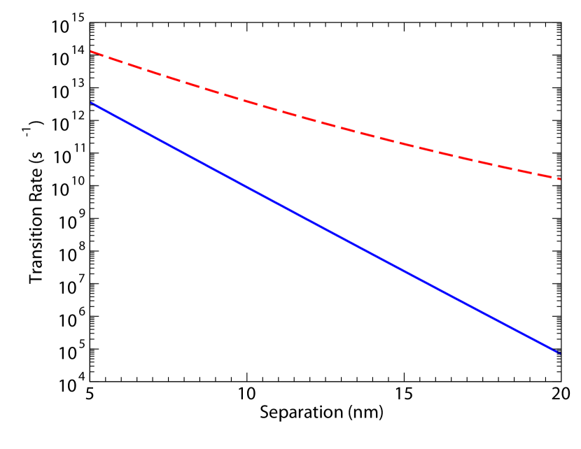
As a plausibility check, we consider the work of Schroeter et al., who computed the tunneling of electrons in a spherical 5 nm radius In0.5Ga0.5As dot to a trap in the GaAs matrix, finding transition rates that vary enormously as the separation between the QD and trap is changed from 10 nm to 20 nm (see Fig. 3 in Ref. Schroeter et al., 1996).
Using the parameters in Ref. Schroeter et al., 1996, the energy level of the trap, which is modeled as a delta function potential, lies between the ground and first excited levels of the QD. We computed the electron transition rates from the first excited state of the QD (labeled ) to the trap (labeled ), and from the trap to the ground state of the QD (labeled . The results as a function of the separation between the QD and the trap are shown in Fig. S7. The transition rate varies from s-1 to s-1 for dot-trap separations of 5 nm to 20 nm, while the rate varies from over s-1 to less than s-1. The strong variation in tunneling rates over this distance range is consistent with the wide range of transition rates produced in the rate equation model fits to the data from the main text.
Stark shifts of the QD energy levels, created when carriers populate nearby traps, could be another physical mechanism involved. One resulting phenomenon would be spectral diffusion, that is, a fluctuation in the QD emission frequency. For such spectral diffusion to result in an intensity fluctuation (blinking), its magnitude would need to be on the order of the optical filter bandwidth we use (250 eV) when spectrally isolating the QD emission. Recently, Houel and colleauges Houel et al. (2012) have experimentally and theoretically studied spectral diffusion in InAs/GaAs QDs, and predict a Stark shift of 20 eV when a single carrier (hole) is situated within a couple of nm of the QD. Presumably multiple defect states would need to be simultaneously filled to reach shifts large enough to move the QD emission frequency outside of our filter window. In such a scenario, a wide range of timescales for spectral diffusion could lead to the observed results. For example, Abbarchi et al. have recently studied spectral diffusion in GaAs QDs through a correlation function approach, and fit their data to a function whose long-time scale behavior (i.e., at times much greater than the QD radiative lifetime) is given by a standard diffusion expression, meant to represent the displacement of a charge carrier near the QD Abbarchi et al. (2012). Plotted on a logarithmic time scale, this function shows a shoulder reminiscent of those seen in Figs. 2-4 in the main text. One could then envision a model consisting of multiple charge carriers, each causing Stark shifts to the QD emission energy and exhibiting diffusive motion with a different characteristic timescale, as producing qualitatively similar curves as the data we have measured in Figs. 2-4 in the main text. On the other hand, the precise time-dependent behavior of the diffusive motion does not agree with our data (diffusive motion has wider tails), and the requirement of multiple diffusive timescales disagrees with the observation made in Ref. Abbarchi et al., 2012, where a single diffusion time constant was used to model data from multiple quantum dots, and from this it was inferred that the behavior of the carrier diffusion was independent of the specific local environment.
Finally, we note that strong perturbation of the electron and hole wavefunctions due to the nearby charges has also been considered as a mechanism for blinking, by Sugisaki and colleagues Sugisaki et al. (2001), and if incorporated alongside a model for trap filling dynamics, might provide an alternative explanation for what we have observed.
X Blinking probability distributions
As pointed out in Lippitz et al. (2005), correlation functions can reveal the kinetics of the blinking signal over a large time range, however, they only provide averaged information about the distributions of bright and dark time intervals. Alternatively, probability distributions for the instantaneous intensity fluctuations can in principle be obtained from photon-counting histograms, providing complementary information for the characterization of single emitters. This technique is commonly done in the blinking literature Lippitz et al. (2005); Stefani et al. (2009); Crouch et al. (2010), and has been applied towards epitaxially-grown quantum dots Pistol et al. (1999); Sugisaki et al. (2001); Wang et al. (2005). In the latter case, exponential blinking time distributions have been reported, which suggests coupling of the quantum dots to neighboring two-level systems Fleury et al. (1993). Such behavior contrasts with that of nanocrystal quantum dots, which are known to display power-law type distributions Crouch et al. (2010).
In what follows, we attempt to extract the probability distributions of blinking intervals for a single quantum dot in one of our fabricated devices. The results of Ref. Crouch et al. (2010) suggest that reliable recovery of blinking probability distribution functions require that intensity histograms display clear bimodal distributions, with two non-overlapping peaks corresponding to dark and bright emitter states, and time trajectories with several thousands of blinking events; these criteria must furthermore be met for bin sizes varying over at least a decade. Only one of our measured devices (Device 1) produced histograms with clear bimodal distributions, as shown in Fig. S8(a)-(c), for bin widths varying over almost a decade (from 5 ms up to 40 ms).
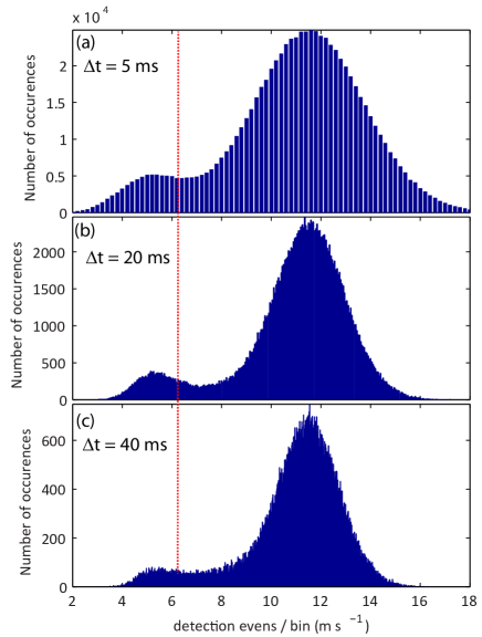
Although it is clear that there is some overlap between the bright and dark histogram peaks, we proceed to analyze the probability distributions of the ’on’ and ’off’ time intervals of this device. We start by defining an emission rate threshold for the binned data, below which the dot was considered to be in a dark or ’off’ state, and, above it, in a bright or ’on’ state it. Histograms of the durations of ’off’ and ’on’ state intervals were produced, and fitted on a log scale to a linear polynomial using a least-squares routine. Before fitting, the statistical weighting scheme of refs. Crouch et al. (2010); Kuno et al. (2001) was applied to the raw data, which produced the following probability distributions:
| (S5) |
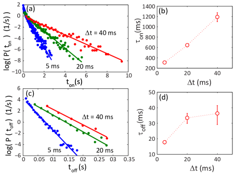
Here, is the number of ’off’ or ’on’ events of duration , is the total number of events in the time series, and is the average time interval between next neighbor events. This weighting is done to provide better statistical estimates for the probability distributions at long times, where the data is noisy and very sparse due to the finite duration of the measurement. Figures S9(a) and (b) respectively show ’on’ and ’off’ state time interval distributions for 5 ms, 20 ms and 40 ms, for an intensity threshold indicated by a red dashed line in Figs. S8(a)-(c). Here, is equidistant, in standard deviations, from the ’on’ and ’off’ intensities Lippitz et al. (2005):
| (S6) |
The closeness of the fits to the experimental data suggest that the ’on’ and ’off’ time probability distributions are single exponential, however it is evident that the characteristic times differ by a significant amount for different values. To understand how much data processing influences the results, Figs. S10(a) and (b) show the range of characteristic times ( and ) obtained, as a function of , for bin widths between 5 ms and 40 ms. The thick lines in the figures correspond to averages over all , at each . The mean characteristic time for the ’on’ state is seen to vary widely, from close to 1330 ms for at the low intensity peak, to near 100 ms for at the high intensity peak, and a similar behavior is observed for the ’off’ times. Primarily, this large variation has to do with the quality of the fits, which we evaluate through the 95 confidence intervals. For the single exponential functions , we plot, in Figs. S10(c), the figure of merit
| (S7) |
averaged over all bin widths .
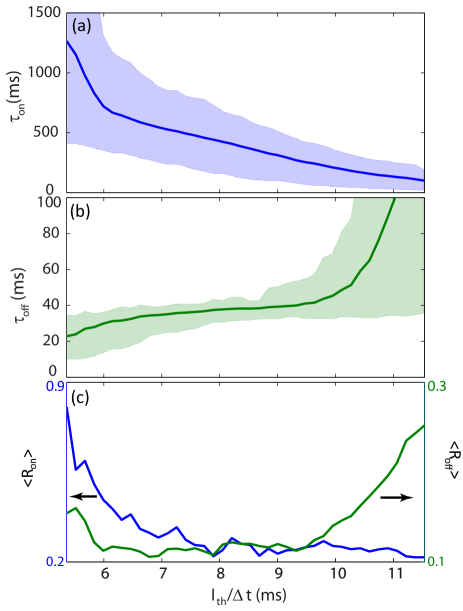
In eq.(S7), and are the 95 fit confidence intervals. Evidently, the overall fit quality for ’on’ and ’off’ times decreases significantly as approaches and respectively, and reaches a baseline as moves towards the opposite extremes. Due to the overlap between the bright and dark peaks in the histograms of Figs. S8(a)-(c), ’on’ and ’off’ times are related through , and so we may establish that reliable characteristic times can be found only within intervals for which are simultaneously minimized. Within the interval 7 ms ms-1, ranges between 25 ms and 50 ms, and between 100 ms and 850 ms.
In summary, our analysis of the blinking trajectories shows that, within valid threshold and bin size ranges, ’on’ and ’off’ time distributions can be reasonably well-fit to single exponentials, as observed in other self-assembled quantum dots; it is clear that the probability distributions do not follow power laws as is the case for colloidal dots. On the other hand, the uncertainties for the characteristic times are very wide, as extracted values vary significantly with the choice of intensity threshold. This limitation is strongly related to the poor resolution of the ’on’ and ’off’ peaks, which is indeed maximized over only a small range - at most a decade - of bin widths. An additional issue for the ’off’ times distribution is that the bin sizes over which peak resolution is clear are comparable to the ’off’ time characteristic times, while, ideally, for good resolution of blinking events. As noted in Crouch et al. (2010), it is apparent that blinking trajectory analysis requires a very stringent set of conditions for the data, so that reliable information may be extracted regarding the on/off time distributions. This contrasts with the correlation analysis performed in the main text, which is known to produce reliable quantitative information when directly applied to raw data Lippitz et al. (2005) - albeit not directly providing information about the blinking interval distributions.
References
- Malik et al. (1997) S. Malik, C. Roberts, R. Murray, and M. Pate, Appl. Phys. Lett. 71, 1987 (1997).
- Davanço et al. (2011) M. Davanço, M. T. Rakher, D. Schuh, A. Badolato, and K. Srinivasan, Appl. Phys. Lett. 99, 041102 (2011).
- Ates et al. (2012) S. Ates, L. Sapienza, M. Davanço, A. Badolato, and K. Srinivasan, IEEE J. Sel. Top. Quan. Elec. 18, 1711 (2012).
- Lin et al. (2006) S. W. Lin, A. M. Song, N. Rigopolis, B. Hamilton, A. R. Peaker, and M. Missous, J. Appl. Phys. 100, 043703 (2006).
- Ates et al. (2013) S. Ates, I. Agha, A. Gulinatti, I. Rech, A. Badolato, and K. Srinivasan, Scientific Reports 3, 1397 (2013).
- Freedman and Diaconis (1981) D. Freedman and P. Diaconis, Probability Theory and Related Fields 57, 453 (1981).
- Laurence et al. (2006) T. A. Laurence, S. Fore, and T. Huser, Opt. Lett. 31, 829 (2006).
- Carmichael and Walls (1976) H. J. Carmichael and D. F. Walls, Journal of Physics B: Atomic and Molecular Physics 9, 1199 (1976).
- Hellberg and Manousakis (2000) C. S. Hellberg and E. Manousakis, Phys. Rev. B 61, 11787 (2000).
- Molski et al. (2000) A. Molski, J. Hofkens, T. Gensch, N. Boens, and F. De Schryver, Chem. Phys. Lett. 318, 325 (2000).
- Spinicelli et al. (2009) P. Spinicelli, S. Buil, X. Quélin, B. Mahler, B. Dubertret, and J.-P. Hermier, Phys. Rev. Lett. 102, 136801 (2009).
- Lin et al. (2005) S. W. Lin, C. Balocco, M. Missous, A. R. Peaker, and A. M. Song, Phys. Rev. B 72, 165302 (2005).
- Asano et al. (2010) T. Asano, Z. Fang, and A. Madhukar, J. Appl. Phys. 107, 073111 (2010).
- Schroeter et al. (1996) D. F. Schroeter, D. J. Griffiths, and P. C. Sercel, Phys. Rev. B 54, 1486 (1996).
- Houel et al. (2012) J. Houel, A. V. Kuhlmann, L. Greuter, F. Xue, M. Poggio, R. J. Warburton, B. D. Gerardot, P. A. Dalgarno, A. Badolato, P. M. Petroff, A. Ludwig, D. Reuter, and A. D. Wieck, Phys. Rev. Lett. 108, 107401 (2012).
- Abbarchi et al. (2012) M. Abbarchi, T. Kuroda, T. Mano, M. Gurioli, and K. Sakoda, Phys. Rev. B 86, 115330 (2012).
- Sugisaki et al. (2001) M. Sugisaki, H.-W. Ren, K. Nishi, and Y. Masumoto, Phys. Rev. Lett. 86, 4883 (2001).
- Lippitz et al. (2005) M. Lippitz, F. Kulzer, and M. Orrit, ChemPhysChem 6, 770 (2005).
- Stefani et al. (2009) F. D. Stefani, J. P. Hoogenboom, and E. Barkai, Physics Today 62, 34 (2009).
- Crouch et al. (2010) C. H. Crouch, O. Sauter, X. Wu, R. Purcell, C. Querner, M. Drndic, and M. Pelton, Nano Letters 10, 1692 (2010).
- Pistol et al. (1999) M.-E. Pistol, P. Castrillo, D. Hessman, J. A. Prieto, and L. Samuelson, Phys. Rev. B 59, 10725 (1999).
- Wang et al. (2005) X. Y. Wang, W. Q. Ma, J. Y. Zhang, G. J. Salamo, M. Xiao, and C. K. Shih, Nano Letters 5, 1873 (2005).
- Fleury et al. (1993) L. Fleury, A. Zumbusch, M. Orrit, R. Brown, and J. Bernard, Journal of Luminescence 56, 15 (1993).
- Kuno et al. (2001) M. Kuno, D. P. Fromm, H. F. Hamann, A. Gallagher, and D. J. Nesbitt, The Journal of Chemical Physics 115, 1028 (2001).