Effect of Thermal Annealing on Boron Diffusion, Micro-structural, Electrical and Magnetic properties of Laser Ablated CoFeB Thin Films
Abstract
We report on Boron diffusion and subsequent crystallization of Co40Fe40B20 (CoFeB) thin films on SiO2/Si(001) substrate using pulsed laser deposition. Secondary ion mass spectroscopy reveals Boron diffusion at the interface in both amorphous and crystalline phase of CoFeB. High-resolution transmission electron microscopy reveals a small fraction of nano-crystallites embedded in the amorphous matrix of CoFeB. However, annealing at 400∘C results in crystallization of CoFe with bcc structure along (110) orientation. As-deposited films are non-metallic in nature with the coercivity (Hc) of 5Oe while the films annealed at 400∘C are metallic with a Hc of 135Oe.
pacs:
XX-XX, XX-XX-XXI Introduction
(CoxFe1-x)80B20 alloys have been under extensive research focus due to high tunneling magnetoresistance (TMR)and perpendicular magnetic anisotropy (PMA) observed in thin films of this material combined with ultrathin MgO layerS. Ikeda1 ; W. G. Wang1 ; W. G. Wang2 ; S. Ikeda2 . A controlled transition of CoFeB from amorphous to crystalline phase is a necessary condition for the observation of giant TMR effectS. Ikeda1 ; W. G. Wang1 ; W. G. Wang2 . By post deposition thermal annealing in vacuum, TMR of the CoFeB based magnetic tunnel junctions (MTJs) increases abruptlyW. G. Wang2 . Furthermore, recent resultsS. Ikeda2 have shown that although CoFeB/MgO system is widely used for in-plane-anisotropy MTJs, it can also meet the requirements of high thermal stability and low induced current density magnetization switching for high performance perpendicular MTJs. Apart from this, CoFeB has lower coercivity (Hc)C. Y. You , high spin dependent scatteringK. Nagasaka , stronger spin tunneling effectS. Ikeda1 , and therefore, supports a higher output signal for particular giant magnetoresistance (GMR) and TMR ratios in CoFeB electrode based MTJs.
From the reported results, there is a sharp contradiction in opinions on TMR ratios due to Boron diffusion at the interface between ferromagnetic electrode and tunnel barrier. Earlier studiesJ. J. Cha ; S. S. Mukherjee ; J. C. Read have shown that improvement of TMR results from Boron diffusion at the interface of CoFeB and tunnel barrier during annealing because it forms an energetically favorable poly-crystalline Mg-B-O layer in case of CoFeB/MgO interface, whereas other groupsJ. D. Burton ; T. Miyajima ; X. Kozina ; H. D. Gan have claimed that Boron enrichment in the barrier is detrimental to TMR because it significantly suppresses the majority-channel conductance. Furthermore, crystallization of amorphous CoFeB during thermal annealing at the interface has been reported to be sensitive to its TMR effect due to enhance coherent tunnelingW. G. Wang1 ; S Yuasa ; J. Hayakawa . However, crystallization of CoFeB electrode and change in the barrier properties due to Boron diffusion at the interface during annealing have not been fully characterized and understood till now. Therefore, it is important to study in detail of what happens to Boron at the interface of SiO2/CoFeB as a function of the degree of crystallization with respect to its original amorphous phase.
To date, CoFeB thin films have been grown by using different sputtering methods such as dc, rf and Ion beam sputteringShinji Yuasa ; M. Raju . Electron beam evaporation of CoFeB thin film has also been employed successfullyJ. J. Cha . However, there are no reports on pulsed laser deposited (PLD) thin films and junctions. The electron energy-loss spectroscopy and x-ray photo electron spectroscopy of CoFeB/MgO/CoFeB MTJs reveals that the existence of Boron as BOx in the barrier layer depends on the deposition methodJudy J. Cha ; Abdul . In the present study, we have explored PLD technique as it offers a unique advantage for the growth of multi-elemental films of desired stoichiometry of the elements with widely varying vapour pressures. CoFeB films can be either amorphous or nano crystalline depending on the thermal treatment, composition of the elements and film thicknessY. M. Lee . We carried out Secondary ion mass spectroscopy (SIMS) depth profile measurements to investigate the diffusion of constituent elements especially the Boron. High-resolution transmission electron microscopy (HRTEM) observations reveal that CoFeB crystallized upon annealing at 400∘C. The present work also focuses on to correlate annealing effects on micro-structural, electrical transport and magnetic properties of CoFeB thin films grown on amorphous layer of SiO2 coated on (001) Si substrate.
II Experimental
A KrF excimer laser that produces laser pulses of width 20 ns and wavelength of 248 nm operated at a repetition rate of 10 Hz was used to ablate a stoichiometric target of Co40Fe40B20(at%). The intensity of laser plume produced an aerial energy density of 4 Jcm-2/pulse. The PLD deposition chamber was evacuated to the base pressure of 2x10⁻⁷ mbar prior to deposition. The deposition pressure was kept at 2.5x10⁻³ mbar. 6N purity Ar gas was used as a buffer gas. Under these conditions, a deposition rate of 0.4 Ås-1 was realized. The films were annealed immediately after the deposition in the same chamber at 200, 300 and 400∘C for 1 hour under high vacuum. Our PLD grown films are highly consistent and reproducible. Crystallographic structure of the films was characterized using a PANalytical X’Pert PRO MRD X-ray diffractometer with CuK1 radiation. Elemental analysis was carried out on a Rigaku ZSX Primus II Wavelength Dispersive X-ray Fluorescence Spectrometer (WD-XRF). The stoichiometry of the film as estimated by WD-XRF analysis is within the correct stoichiometry of the target. HRTEM experiments were carried out by employing a FEI Tecnai G2 F30 STWIN field emission gun supported 300 kV microscope. The depth profiled data was obtained by using TOF-SIMS 5 (ION-TOF GmbH, Germany). Resistivity measurements were carried out in the standard four probe geometry over a temperature range of 5-300K in a closed cycle refrigerator. Magnetization of the samples was measured at room temperature by using EV7 model Vibrating Sample Magnetometer (VSM).
III Results and discussions
III.1 Structural studies
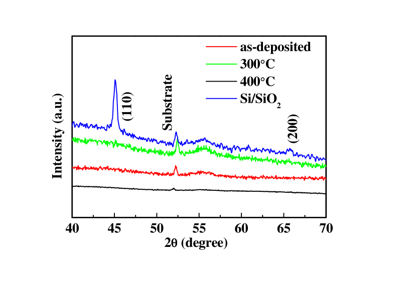
Grazing incident angle X-ray diffraction (GIXRD) patterns of the as-deposited and annealed films of 40 nm thickness are shown in Fig.1. The absence of any Bragg peak in the GIXRD scans suggests that the as-deposited and the films annealed up to 300∘C are amorphous in nature. But the samples annealed at 400∘C shows a peak at 2 = 45.07∘ which is attributed to CoFe with bcc structure along (110) orientation. A broad diffused peak centered at around 65.7∘ shows an evidence of the (200) reflection. Our HRTEM results also show similar kind of reflection at atomic scale in both as-deposited and annealed samples. The average crystallite size of the films is determined by the Scherrer formula is about 20 nm for annealed films at 400∘C. Strain induced in the film is calculated by Williamson-Hall method using the formula: , where is the full width at half-maximum in radians, is the Bragg diffraction angle of the peak, is the Scherrer constant, is the wavelength of the X-rays and is the crystallite size estimated from HRTEM results. The films have tensile strain of -2.44x10⁻⁴ generated due to vacancy-type imperfections known as Schottky defects in the lattice created presumably by leaving Boron into the interface.
III.2 SIMS depth profiles
A uniform distribution of Co and Fe is clearly seen across the thickness of as-deposited and annealed film (Fig.2). The peak of Boron intensity profile (black in color) indicates strong Boron segregation at the apex of the interface of SiO2/CoFeB. It is interesting to note that while sputtered CoFeB films suggests the presence of Boron in amorphous phaseA. A. Greer ; S. V. Karthik , our PLD grown films in as-deposited state confirms that Boron segregates and resides at the interface leaving CoFe in amorphous phase. The Si signal starts rising at around 30 nm and becomes constant at 50 nm which indicates an out-diffusion of Si into the film structure. The Cobalt, Iron and Boron signals tends to reduce after 40 nm which is typically the film thickness but they are found to diffuse into the substrate as well. Si diffusion into the film is comparatively less and it becomes constant at 44 nm in the annealed film. The diffusion of Cobalt, Iron and Boron into the substrate is observed to be more in the annealed sample as it is clearly visible in the depth profile. The reported results on first principle calculationsJ. D. Burton stated that rather than inside the CoFe matrix, segregation of Boron at the interface is energetically favorable which is consistent for our PLD grown amorphous films.
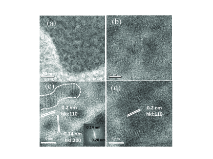
The HRTEM micrograph of the as-deposited samples in general shows a feature-less contrast of amorphous phase in Fig.3(a). In some selective regions dispersed in the microstructure, little crystalline zones have been noted [Figs.3(b) and (c)]. Further, the microstructure observed in these regions reveals some interesting ultra-fine details. In Fig.3(c), it is evident that the crystalline regions are in selectively embedded state in the amorphous matrix. A faint contrast of atomic planes in Fig.3(c) further authenticates the significant fraction of amorphous phase surrounding the crystalline phase, which is negligible compared to large fraction of amorphous structure in the matrix. A region surrounded by white dotted line displays a set of moiré fringes evolved due to overlapping of ultra-thin tiny crystals (Fig.3c). The careful measurement of inter planar spacings (dhkl) between the planes in Fig.3(c) yields (dhkl) of 0.2 and 0.14 nm, which corresponds to hkl indices of (110) and (200), respectively of a cubic cell (lattice parameter: a = 0.29 nm, space group: Pm3̄m, PDF card no. 00-044-1433). A corresponding fast fourier transform (FFT) recorded from these nano-crystallites in an aggregate exhibits that the nano-crystallites are in random orientation with respect to each other and lead to Debye rings in reciprocal space. The presence of the inter-planar spacings of 0.2 and 0.14 nm corresponding to the planes (110) and (200) respectively are marked on FFT pattern (inset in Fig.3c). A relatively more intense plane with higher fraction compared to (200) planes was the existence of (110) set of atomic planes in the microstructure with the inter-planar spacings of about 0.2 nm in Figs.3(c) and (d). Lattice scale images of (110) planes in the amorphous matrix reveals a better grey level contrast (Fig.3d) compared to that of (200) planes (Fig.3c).
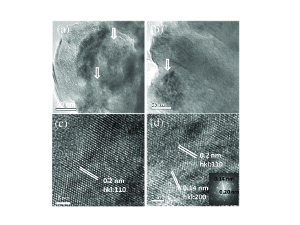
The overall microstructure of annealed film at 400∘C as shown in Figs.4(a) to (d) has a distinct grey level contrast consists of several nano-crystallites of the size even up to 15 to 20 nm. These nano-crystallites marked with a set of white arrows [Figs. 4(a) and (b)] are separated from each other with apparent interface of the boundary length between 5 to 10 nm. It is evident that the film microstructure is aligned preferably along the well oriented atomic planes of (110), a cubic crystal within individual nano-crystallites. The dominant atomic planes in the matrix are observed as (110) although the formation of (200) planes exists [Figs.4(c) and (d)]. A corresponding FFT [inset in Fig.4(d)] further elucidates a set of atomic planes in reciprocal space with inter-planar spacings of 0.29 and 0.14 nm.
III.3 Electrical transport studies
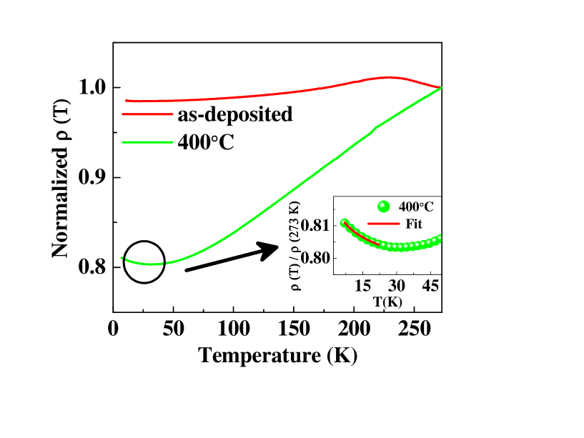
Electrical transport properties of CoFeB films in their as-deposited state and annealed at 400∘C are shown in Fig.5. Resistivity data has been normalized to its value at 273K. The room temperature resistivity of as-deposited films are about 70cm and for samples annealed at 400∘C is observed to be 8cm respectively. The abrupt increase in resistivity values for amorphous films and observed non-metallic behavior could be due to intragrain tunneling and the SiO2 inclusions into the film was reported previously in granular CoFeB-SiO2 amorphous thin film systemP. Johnsson . Our HRTEM results indicate the presence of nano crystalline regions in the amorphous matrix of CoFeB, these crystalline regions are well separated and leading to the absence of metallic channels support the observed transport behavior. The resistivity is found to reduce gradually on decreasing temperature from 300K followed by a clear increase in its value below 22K for the film annealed at 400∘C. A fit to the part of our experimental data below the resistivity minimum for annealed sample using the following empirical relation is shown as a solid line in the figure. Clear agreement with experimental data suggests finite magnetic contribution as has been observed in several amorphous ferromagnetic alloys at low temperatureS. N. Kaul . The detailed analysis of our transport measurements is under progress.
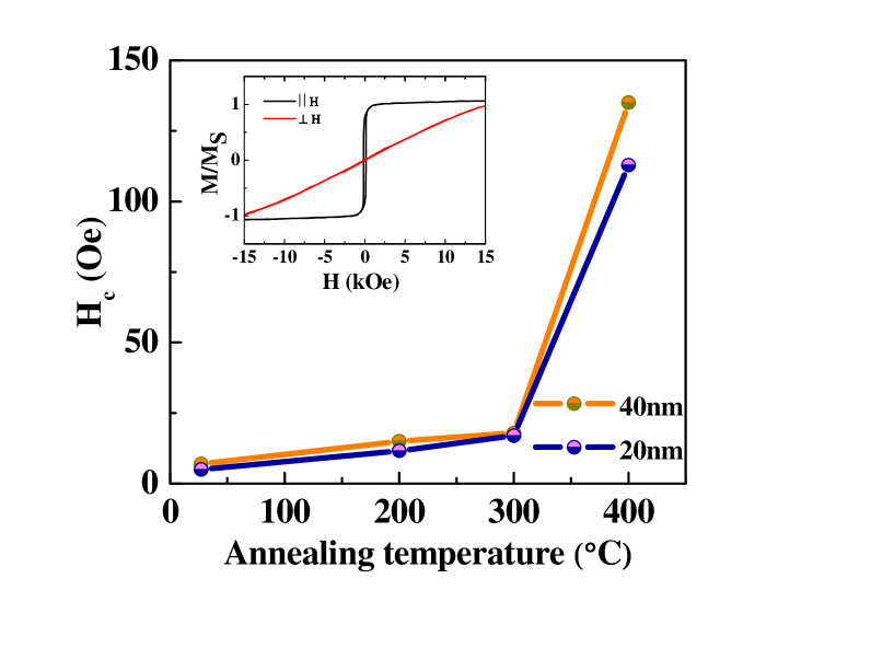
Magnetization [M(T)] measurement performed on as-deposited and annealed CoFeB films at different temperatures are shown in Fig.6. The ferromagnetic hysteresis loops after substrate correction for in-plane and out-of-plane orientations confirmed that films exhibit in-plane easy axis of magnetization. In the annealed film, the easy axis loop is squared shape, while the hard axis of the film displays a much slanted curve indicating the presence of magnetic anisotropyJ. McCord . The as-deposited samples and samples annealed up to 300∘C shows Hc of 10Oe. The films annealed at 400∘C are found to show increase in Hc from 5Oe to 135Oe. A sharp increase in Hc at annealing temperature of 400∘C is a clear evidence of crystallization of amorphous CoFeB films.
IV Conclusions
In summary, we have grown thin film of CoFeB using pulsed laser ablation of an alloy target. HRTEM together with resistivity measurements reveal that annealing at 400∘C increases the metallicity of the film by forming nano-crystallites. The sudden increase in Hc from 5Oe to 135Oe after annealing at 400∘C also confirms the crystallization of CoFeB. Magnetic hysteresis loops of in-plane and out-of-plane measurements reveal that our films have in-plane easy axis of magnetization. We believe Boron segregation at the interface of SiO2/CoFeB, observed in our SIMS depth profiles, have important repercussions on the TMR values.
V Acknowledgments
This research has been supported by Council of Scientific and Industrial Research (CSIR), Government of India. The authors are grateful to Prof. R. C. Budhani, Director NPL for his valuable suggestions. Venkat and Himanshu acknowledge CSIR for financial support.

References
- (1) Ikeda S, Hayakawa J, Ashizawa Y, Lee Y M, Miura K, Hasegawa H, Tsunoda M, Matsukura F and Ohno H 2008 Appl. Phy. Lett. 93 082508
- (2) Wang W G, Ni C, Miao G X, Weiland C, Shah L R, Fan X, Parson P, Jordan-sweet J, Kou X M, Zhang Y P, Stearrett R, Nowak E R, Opila R, Moodera J S and Xiao J Q 2010 Phys. Rev. B. 81 144406
- (3) Wang W G, Jordan-sweet J, Miao G X, Ni C, Rumaiz A K, Shah L R, Fan X, Parsons P, Stearrett R, Nowak E R, Moodera J S and Xiao J Q 2009 App. Phy. Lett. 95 242501
- (4) Ikeda S, Miura K, Yamamoto H, Mizunuma K, Gan H D, Endo M, Kanai S, Hayakawa J, Matsukura F and Ohno H 2010 Nature Matter. 9 721
- (5) You C Y, Goripati H S, Furubayashi T, Takahashi Y K and Hono K 2008 Appl. Phys. Lett. 93 012501
- (6) Nagasaka K, Seyama Y, Varga L, Shimizu Y and Tanaka A 2001 J. Appl. Phys. 89 6943
- (7) Cha J J, Read J C, Egelhoff W F, Huang P Y, Tseng H W, Li Y, Buhrman R A and Muller D A 2009 Appl. Phys. Lett. 95 032506
- (8) Read J C, Cha J J, Egelhoff W F, Jr, Tseng H W, Huang P Y, Li Y, Muller D A and Buhrman R A 2009 Appl. Phys. Lett. 94 112504
- (9) Mukherjee S S, MacMahon D, Bai F, Lee C -L and Kurinec S K 2009 Appl. Phys. Lett. 94 082110
- (10) Burton J D, Jaswal S S, Tsymbal E Y, Mryasov O N and Heinonen O G 2006 Appl. Phys. Lett. 89 142507
- (11) Miyajima T, Ibusuki T, Umehara S, Sato M, Eguchi S, Tsukada M and Kataoka Y 2009 Appl. Phys. Lett. 94 122501
- (12) Kozina X, Ouardi S, Balke B, Stryganyuk G, Fecher G H, Felser C, Ikeda S, Ohno H and Ikenaga E 2010 Appl. Phys. Lett. 96 072105
- (13) Gan H D, Ikeda S, Shiga W, Hayakawa J, Miura K, Yamamoto H, Hasegawa H, Matsukura F, Ohkubo T, Hono K and Ohno H 2010 Appl. Phys. Lett. 96 192507
- (14) Yuasa S and Djayaprawira D D 2007 J. Phys. D: Appl. Phys. 40 R337
- (15) Hayakawa J, Ikeda S, Lee Y M, Matsukura F and Ohno H 2006 Appl. Phys. Lett. 89 232510
- (16) Raju M, Chaudhary S and Pandya D K 2011 Appl. Phys. Lett. 98 212506
- (17) Yuasa S, Suzuki Y, Katayama T and Ando K 2005 Appl. Phys. Lett. 87 242503
- (18) Cha J J, Read J C, Buhrman R A and Muller D A 2007 Appl. Phys. Lett. 91 062516
- (19) Rumaiz A K, Jaye C, Woicik J C, Wang W and Fischer D A 2011 Appl. Phys. Lett. 99 222502
- (20) Lee Y M, Hayakawa J, Ikeda S, Matsukura F and Ohno H 2007 Appl. Phys. Lett. 90 212507
- (21) Greer A A, Gray A X, Kanai S, Kaiser A M, Ueda S, Yamashita Y, Bordel C, Palsson G, Maejima N, Yang S -H, Conti G, Kobayashi K, Ikeda S, Matsukura F, Ohno H, Schneider C M, Kortright J B, Hellman F and Fadley C S 2012 Appl. Phys. Lett. 101 202402
- (22) Karthik S V, Takahashi Y K, Ohkubo T, Hono K, Ikeda S 2009 J. Appl. Phys. 106 023920
- (23) Johnsson P, Aoqui S I, Grishin A M and Munakata M 2003 J. Appl. Phys. 93 8101
- (24) Kaul S N, Kettler W and Rosenberg M 1986 Phys. Rev. B 33 4987
- (25) McCord J, Mattheis R and Elefant D 2004 Phys. Rev. B 70 094420
VI List of Figures
FIG.1. GIXRD measurements of bare substrate (Si/SiO2) and
Co40Fe40B20 thin film of thickness 40
nm in as-deposited and annealed states.
FIG.2. Secondary Ion Mass Spectroscopy (SIMS) depth profiles of
as-deposited and annealed CoFeB thin films of 40 nm thick at
400∘C showing strong Boron (B) diffusion at the interface.
FIG.3. HRTEM micrographs of CoFeB as-deposited film showing (a)
amorphous phase, (b - d) a small fraction of nano-crystallites
distributing in the dominated amorphous matrix. Inset in (c) shows
a corresponding FFT in reciprocal space.
FIG.4. HRTEM micrographs of CoFeB film annealed at 400∘C
showing (a - b) crystalline microstructure, (c - d) atomic planes
of crystalline phase constituting the entire matrix of the film.
Inset (d) shows a corresponding FFT in reciprocal space.
FIG.5. Normalized resistivity graph of Co40Fe40B20
as-deposited and annealed films. Inset shows zoomed image of the
electrical resistivity of 400∘C annealed film. The solid
line in the inset represents fit to the equation in the
temperature range of 7-22K.
FIG.6. Hc plots as a function of annealing temperature for
CoFeB of thickness 40 and 20 nm. Inset shows the room temperature
magnetic hysteresis loops for 400∘C annealed film measured
along parallel and perpendicular field direction with respect to film plane.