Manipulating chiral transmission by gate geometry: switching in graphene
with transmission gaps
Abstract
We explore the chiral transmission of electrons across graphene heterojunctions for electronic switching using gate geometry alone. A sequence of gates is used to collimate and orthogonalize the chiral transmission lobes across multiple junctions, resulting in negligible overall current. The resistance of the device is enhanced by several orders of magnitude by biasing the gates into the bipolar doping regime, as the ON state in the near homogeneous regime remains highly conductive. The mobility is preserved because the switching involves a transmission gap instead of a structural band-gap that would reduce the number of available channels of conduction. Under certain conditions this transmission gap is highly gate tunable, allowing a subthermal turn-on that beats the Landauer bound on switching energy limiting present day digital electronics.
The intriguing possibilities of graphene derive from its exceptional electronic and material properties Castro Neto et al. (2009); Das Sarma et al. (2011); Beenakker (2008), in particular its photon-like bandstructure Zhou et al. (2006), ultrahigh mobility Bolotin et al. (2008), pseudospin physics and improved 2-D electrostatics Unluer et al. (2011). Its switching ability, however, is compromised by the lack of a band-gap Schwierz (2010), while opening a gap structurally kills the available modes for conduction, degrading mobility Tseng and Ghosh (2010); Schwierz (2010). This begs the question as to whether we can significantly modulate the conductivity of graphene without any structural distortion, thereby preserving its superior mobility and electron-hole symmetry. A way to do this is to open a transmission gap that simply redirects the electrons, without actually shutting off the density of states. The dual attributes that help graphene electrons in this regard are its photon like trajectories and chiral tunneling that makes the junction resistance strongly anisotropic, allowing redirection with gate geometry alone.
In an earlier paper, Sajjad and Ghosh (2011) we outlined how we can open a transmission gap by a tunnel barrier, angularly injecting the electrons with a quantum point contact (QPC) and then selectively eliminating the low incidence angle Klein tunneling Katsnelson et al. (2006) modes with a barrier, in that case a patterned antidot or an insulating molecular chain. When the critical angle for total internal reflection is lower than the angle subtended at the QPC by the barrier, electrons are unable to cross over across the junction. The result is a transmission gap that can be collapsed by driving the voltage gradient across the junction towards the homogenous or limit, creating a subthermal turn-on sharper than the Landauer binary switching limit of for distinguishability ( for each decade rise in current). Beyond proof of concept, that geometry was limited by a paucity of QPC modes and the structural distortions near the barrier that create a larger effective footprint.
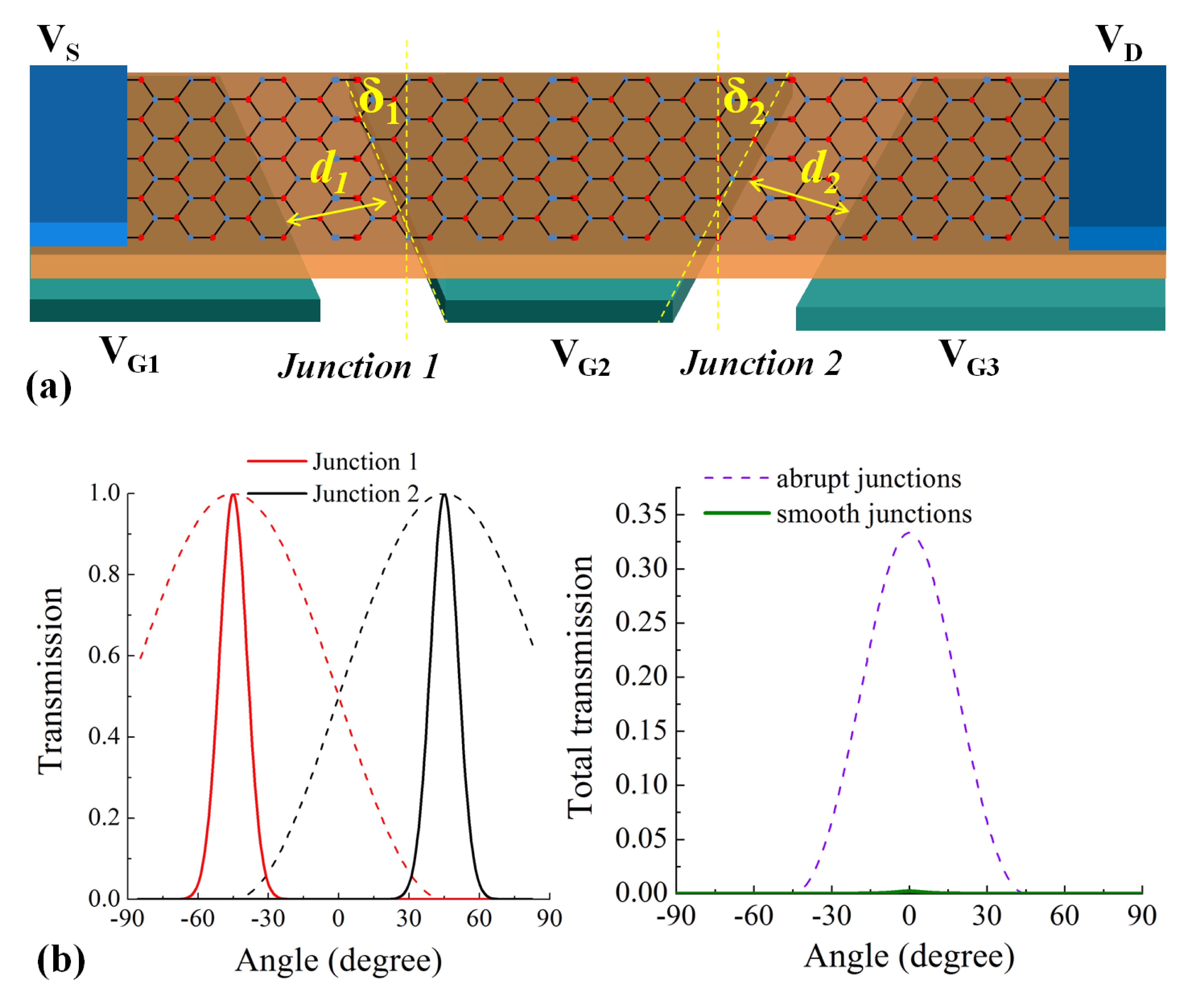
In this paper, we combine a split gated junction to collimate the transverse modes Fig. 1(a), with recently demonstrated Sutar et al. (2012); Sajjad et al. (2012) action of a tilted junction that increases the effective angle of incidence of the electrons. The conductance at zero temperature can be written as,
| (1) |
where is the conductance quantum for two spins, is the number of modes, is transmission of individual modes and is the average transmission over all modes. If all modes transmit with equal probability (), the conductance can simply be written as . Due to the chiral nature of carriers in graphene, transmission in GPNJ is highly angle (mode) dependent making it necessary to work with the average transmission per mode . Instead of eliminating the mode count as does a structural band-gap, we exploit instead the chiral tunneling that makes vanishingly small over a range of energy and controllable with geometry alone (Fig. 1b,c). All modes are available for conduction in the ON state when the split gates are set to the same polarity and thus retaining high mobility of graphene.
Engineering transmission gap with gate geometry. Fig. 1 shows two junctions tilted in opposite directions. Each junction exploits chiral tunneling that conserves pseudospin index and maximizes transmission at normal incidence (Klein tunneling), especially when they are smooth, i.e., the to transition occurs over a finite distance . A tilted junction rotates the transmission lobe accordingly, Sajjad et al. (2012), shifting transmissions along opposite directions to make them orthogonal. The mode-averaged transmissions across the dual junction can be decomposed as below (see appendix for details)
| (2) | |||||
| (3) | |||||
which is vanishingly small for moderate doping (Fermi wave-vector, , is a constant, ), gate split and tilt angle . The first equation arises from matching pseudospinors across the junction, and denoting components to left and right of a junction (1,2) . The tilt angle modifies the incident angle by and the angle of refraction is related to incident angle through Snell’s law, . The second equation assumes resistive addition of the junction resistances and ballistic flow in between. The mode count for an Ohmic contacted sample of width is given by . The resulting total conductance is negligible in the entire junction regime, indicating that the transmission gap () exists if the carrier densities have opposite polarities,
| (4) |
where is the gate induced voltage step across the junction. This is because the high resistance is primarily contributed by the WKB exponential factor which is valid in the regime, whereas the unipolar regime has only the cosine prefactors represeting the wavefunction mismatch Sajjad et al. (2013).
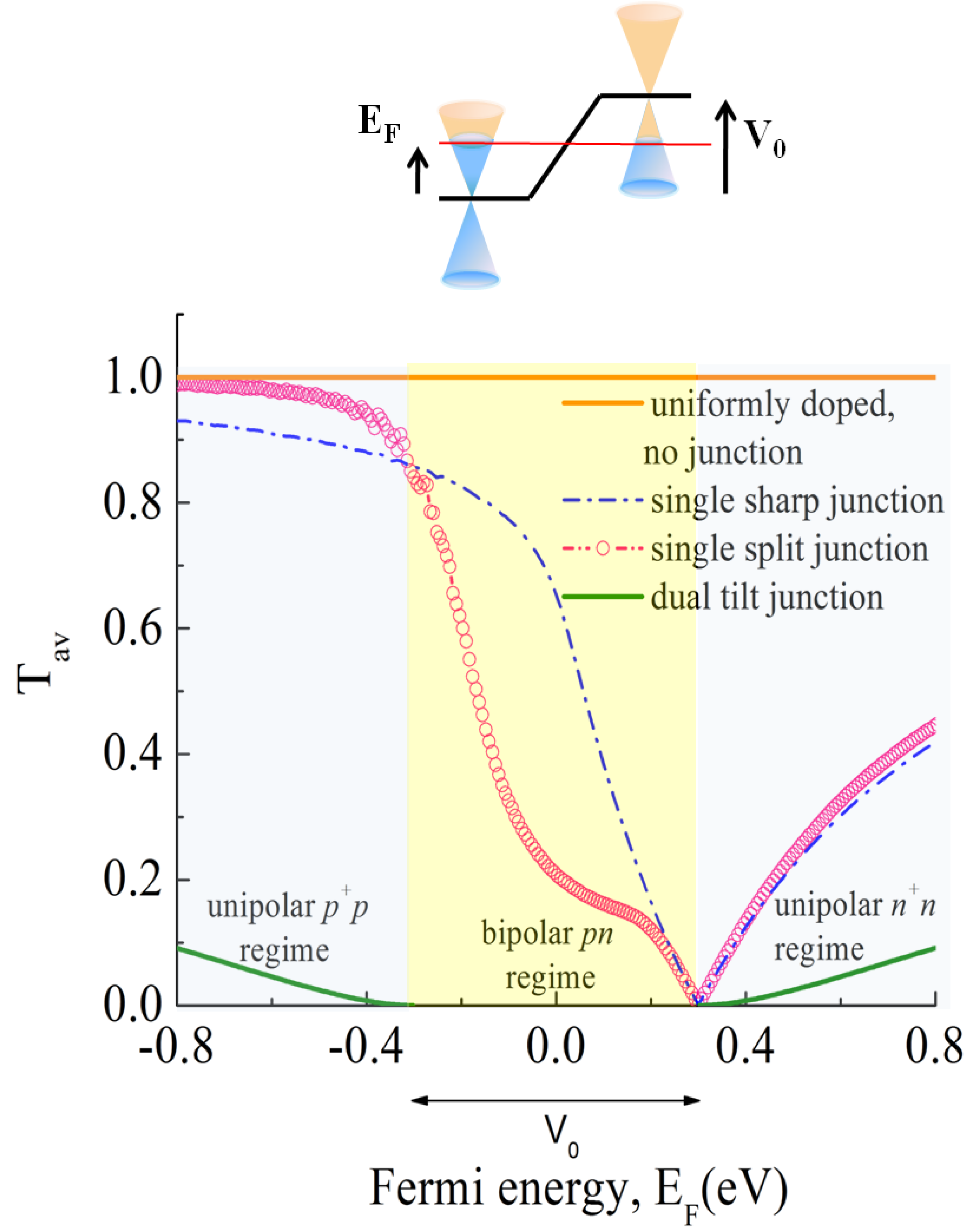
Fig. 2 shows variation of numerically calculated from Eq. Manipulating chiral transmission by gate geometry: switching in graphene with transmission gaps as a function of Fermi energy () for four different devices and doping profiles. The orange line shows unit transmission of all modes for a ballistic uniformly doped graphene sheet. The angular (mode dependent) transmission is manifested in a single sharp ( = 0) graphene junction and the is suppressed (blue dots). Further suppression is achieved with a split junction (pink circles) (non-zero ) due to high transverse energy (mode) filtering. for the device in Fig. 2(a) is shown in green, showing a negligible transmission over the bipolar doping regime. Note that both green and pink lines show suppression only in the bipolar doping regime, outside which the exponential scaling in Eq.Manipulating chiral transmission by gate geometry: switching in graphene with transmission gaps is eliminated Sajjad et al. (2013).
The minimum current is achieved in regime (OFF state). Over the energy window set by the drain voltage , varies weakly, so that the OFF state current at zero temperature for the configuration can be extracted from
| (5) |
convolved with the thermal broadening function at finite temperature. For uniformly doped graphene with ballistic transport,
| (6) |
so that the zero temperature ON-OFF ratio simply becomes,
| (7) |
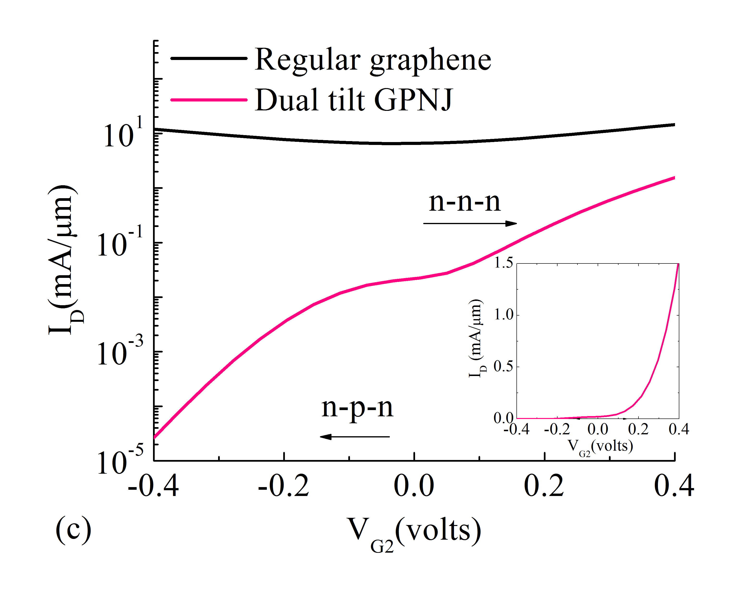
If the biasing is changed all the way from to . Fig. 1(c, pink line) shows the change in dual tilted GPNJ current with gate voltage at room temperature and finite drain bias (), compared with a regular zero bandgap graphene based switch (black line). From the to regime, we see little change in GPNJ current on a log scale. But towards the regime, we see at least three orders of magnitude change when the Fermi window remains mostly within the transmission gap. Compared to the blue line, the ON current is reduced only slightly, while the OFF current is reduced by orders of magnitude. The reduction in ON current comes due to the fact that the doping is not quite uniform at the ON state across the collimator (maintained at unequal doping to avoid a large voltage swing), whereupon the wave-function mismatch leads to lower current than usual. Fully ballistic transport assuming an Ohmic contacted high quality sample gives us an intrinsic ON current in the mA/ regime. In this calculation the gate parameters are , nm, V, V.
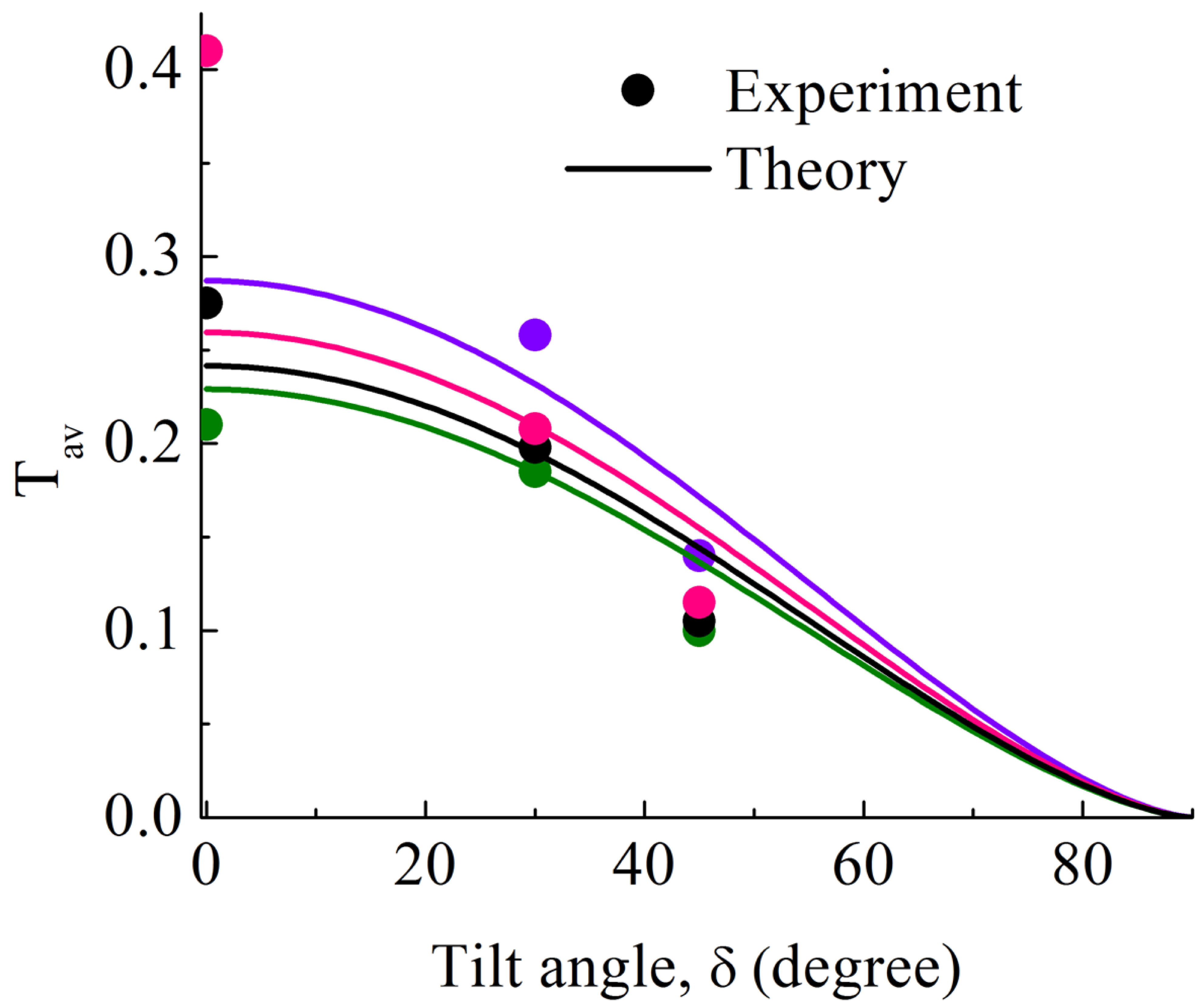
Critical to the geometric switching is the prominance of angle-dependent chiral transmission across a tilted junction, especially in presence of charge puddles and edge reflection. Fig. 3 shows the mode averaged transmission extracted (see method in appendix) from the measured junction resistance for a single split junction, for varying tilt anglesSutar et al. (2012). For an abrupt tilted junction in the symmetric doping limit and represents an electronic analog of optical Malus’ law. The reduction in happens due to the angular shift of transmission lobe (Fig. 1(b)) in low angular mode density region Sajjad et al. (2012). The numerically evaluated generalized for a tilted split junction (solid lines) agrees with experimental data (dots) from all the devices. This angular dependence persists, for multiple diffusive samples Sutar et al. (2012). The scaling of in experiment thus confirms the angular shift of the transmission lobes and forms the basis of the proposed device. The data show a remarkable absence of specular edge scattering, and can be explained by the randomizing effect of roughness.
Modified geometries and impact on subthreshold slope. The aforementioned transmission gap is sensitive to gate parameters. In particular, making one of the junctions abrupt, using overlapping top and bottom gates, produces additional intricacies in addition to the high ON and low OFF current. Both the geometries in Figs. 1 and 4 have junctions aimed at filtering out all propagating modes, but in Fig. 4 the gate split . The abruptness of the second junction makes the critical angle more sensitive to gate voltages and the transmission gap in Eq. 4 needs to be changed. The first junction limits transmission primarily to the Klein tunneling mode Cheianov and Fal’ko (2006) in the OFF state, while the second junction, tilted at (Fig. 4(a)), increases the effective angle of incidence by the gate tilt angle Sajjad et al. (2012)). All the electrons are then reflected if the critical angle of the second junction is less than ,
| (8) |
where and are doping concentrations on the two sides of junction 2. The resulting transmission vanishes over a range of energies (following from Eq. 8), which can be expressed as Sajjad and Ghosh (2011)
| (9) |
analogous to Ref. Sajjad and Ghosh (2011) despite being a different (simpler) geometry, with the tilt angle replacing the barrier angle .
The tunability of the transmission gap for an abrupt junction bears a direct impact on the rate of change of current with gate voltage. For a semiconductor with fixed bandgap, this rate is and limits the energy dissipation in binary switching. The limit arises from the rate of change in overlap between the band-edge and the Fermi-Dirac distribution, normally set by the Boltzmann tail. In our geometry however, the transmission gap is created artificially with a gate bias across the GPNJ, and can be collapsed by going from heterogeneous () towards the homogenous doping limit (). Such a collapsible transport gap will overlap with the Fermi distribution at a higher rate than usual with change in gate bias, leading to a subthermal switching steeper than the Landauer limit. This results a lower gate voltage swing to turn on the device and thus reducing dissipation.
Numerical simulation of quantum flow. To demonstrate carrier trajectories in the proposed device, we numerically solve the Non-Equilibrium Green’s function Formalism (NEGF). The central quantity is the retarded Green’s function,
| (10) |
is the Hamiltonian matrix of graphene, described here with a minimal one orbital basis per carbon atom with eV being the hopping parameter. are the self energy matrices for the semi-infinite source and drain leads, assumed to be extensions of the graphene sheet (i.e., assuming excellent contacts) and are the corresponding anti-Hermitian parts representing the energy level broadening associated with charge injection and removal. is the device electrostatic potential. The current from th atom to h atom is calculated from Datta (1997),
| (11) |
where the electron correlation function, and in-scattering function, . The source and drain Fermi levels are at and . To see the current distribution in the device, we apply a small drain bias . is nonzero only if the th atom and h atom are neighbors. The total current at an atomic site can be found by adding all the components, .
Fig. 4 (right column) shows the local current density. The ON state (bottom right) shows little reflection while the OFF state (top right) shows very little current inside the final wedge connected to the drain. Most of the electrons that do not cross the tilted junction are redirected towards the source by the edges. These electrons, especially the secondary modes, are rejected by the initial collimator and tend to build up in the central wedge. The build-up of charge increases the local quasi-Fermi level until the injection rate at the left junction, set by the transmission rate in Eq. Manipulating chiral transmission by gate geometry: switching in graphene with transmission gaps, equals the leakage rate at the right tilted junction, given by the exponentially reduced tail in Eq. 7 plus additional edge scattering based leakage pathways (a model was presented in Sajjad et al. (2012) including a specularity parameter ).
In summary, by manipuilating the angle dependent chiral tunneling of GPNJ with patterned gates alone, we can controllably suppress Klein tunneling and create a transmission gap as opposed to a structural band-gap. This is accomplished by combining the angular filtering at a split junction with the experimentally demonstrated chiral tunneling across tilted junctions, such that the transmission lobes across multiple junctions become orthogonal to each other in the OFF state. Since the ON state simply requires changing the polarity of the central gate while sticking with otherwise pristine gapless graphene, the ON current stays very high. Furthermore, making the second junction abrupt renders its critical angle and thereby the overall transmission gap highly gate tunable, yielding a subthermal low-voltage turn-on that beats the Landauer switching limit. NEGF simulations show that the OFF current is limited by leakage aided by specular edge scattering, and is limited by build-up and blockade of charge in the central angular wedge.
Acknowledgements.
The authors thank financial support from NRI-INDEX. The authors also thank Frank Tseng (UVa), Chenyun Pan (Georgia Tech), Azad Naeemi (Georgia Tech), Tony Low (IBM), Gianluca Fiori (U Pissa) for useful discussions.References
- Castro Neto et al. (2009) A. H. Castro Neto, F. Guinea, N. M. R. Peres, K. S. Novoselov, and A. K. Geim, Rev. Mod. Phys. 81, 109 (2009).
- Das Sarma et al. (2011) S. Das Sarma, S. Adam, E. H. Hwang, and E. Rossi, Rev. Mod. Phys. 83, 407 (2011).
- Beenakker (2008) C. W. J. Beenakker, Rev. Mod. Phys. 80, 1337 (2008).
- Zhou et al. (2006) S. Y. Zhou, G.-H. Gweon, J. Graf, A. V. Fedrov, C. D. Spataru, R. D. Diehl, Y. Kopelevich, D. H. Lee, S. G. Louie, and A. Lanzara, Nature 2, 595 (2006).
- Bolotin et al. (2008) K. Bolotin, K. Sikes, Z. Jiang, M. Klima, G. Fudenberg, J. Hone, P. Kim, and H. Stormer, Solid State Communications 146, 351 (2008).
- Unluer et al. (2011) D. Unluer, F. Tseng, A. W. Ghosh, and M. R. Stan, Nanotechnology, IEEE Transactions on 10, 931 (2011).
- Schwierz (2010) F. Schwierz, Nat Nano 5, 487 (2010).
- Tseng and Ghosh (2010) F. Tseng and A. W. Ghosh, ArXiv e-prints: 1003.4551 (2010), arXiv:1003.4551 [cond-mat.mes-hall] .
- Sajjad and Ghosh (2011) R. N. Sajjad and A. W. Ghosh, Appl. Phys. Lett. 99, 123101 (2011).
- Katsnelson et al. (2006) M. I. Katsnelson, K. S. Novoselov, and A. K. Geim, Nat Phys 2, 620 (2006).
- Sajjad et al. (2012) R. N. Sajjad, S. Sutar, J. U. Lee, and A. Ghosh, Phys. Rev. B 86, 155412 (2012).
- Low and Appenzeller (2009) T. Low and J. Appenzeller, Phys. Rev. B 80, 155406 (2009).
- Sajjad et al. (2013) R. N. Sajjad, C. Polanco, and A. W. Ghosh, arXiv preprint arXiv:1302.4473 (2013).
- Sutar et al. (2012) S. Sutar, E. S. Comfort, J. Liu, T. Taniguchi, K. Watanabe, and J. U. Lee, Nano Letters 12, 4460 (2012).
- Cheianov and Fal’ko (2006) V. V. Cheianov and V. I. Fal’ko, Phys. Rev. B 74, 041403 (2006).
- Datta (1997) S. Datta, Electronic Transport in Mesoscopic Systems (Cambridge University Press, 1997).
*
Appendix A I
The average tranmsission per mode: Total transmission through a graphene heterojunction can be written as,
| (12) | |||||
Here we have used, angular spacing, , mode spacing and number of modes, . Comparing with Eq. 1, we can write,
| (13) |
Transmission through a single junction, where the potential changes smoothely from to over a distance is given by,
| (14) |
ignoring the wave-function prefactor, this is valid for moderate gate split distance . Let us consider the for a single split junction and a tilted junction separately.
| (15) | |||||
with gate split. For an abrupt tilted junction,
| (16) | |||||
due to reduced density of modes at the higher angular region, is scaled with . Therefore, a resistance measurement () will show an increase for a tilted device.
Transmission through dual tilt GPNJ device: In Fig. 2, we have two such junctions, each of them are tilted. Individual transmissions through the junctions becomes,
| (17) | |||
| (18) |
Since the tilt angle only modifies the angles of the incoming modes.
To get the total transmission, we combine the above two equations ignoring phase coherence to get the total transmission Datta (1997),
| (19) | |||||
Overall transmission becomes
| (20) |
And
| (21) |
For .
Extracting from transport measurement: In the experiment Sutar et al. (2012), the junction resistance is extracted from
| (22) |
The above equation eliminates contact and device resistance due to scatterings and leaves out the resistance contribution from the junction only. Theoretically the total resistance can be divided into two parts (contact and device resistance). From Eq. 1,
| (23) | |||||
| (24) |
In presence of a junction with non-unity , the second term can be considered as the junction resistance,
| (25) |
While the theoretical is already known (Eq. 16), the experimental can be found by plugging the value of from measurement in Eq. 25 . The only unknown value remains is the number of modes at a particular gate voltage.
| (26) |
Here is the shift of Dirac point with gate voltage . The gate capacitance is calculated from a simple parallel plate capacitor model where gate oxide thickness is 100nm.