Three Dimensional Dirac Semimetal and Quantum Transports in Cd3As2
Abstract
Based on the first-principles calculations, we recover the silent topological nature of Cd3As2, a well known semiconductor with high carrier mobility. We find that it is a symmetry-protected topological semimetal with a single pair of three-dimensional (3D) Dirac points in the bulk and non-trivial Fermi arcs on the surfaces. It can be driven into a topological insulator and a Weyl semi-metal state by symmetry breaking, or into a quantum spin Hall insulator with gap more than 100meV by reducing dimensionality. We propose that the 3D Dirac cones in the bulk of Cd3As2 can support sizable linear quantum magnetoresistance even up to room temperature.
pacs:
73.43.-f, 71.20.-b, 73.20.-rI introduction
Weyl semimetal is a new topological state of three-dimensional (3D) quantum matters weyl ; volovik ; monopole ; wan ; HgCrSe ; balents , different from the 3D topological insulators (TI) TIreview ; TIreview-2 ; Bi2Se3 . It can be characterized by Weyl nodes (at Fermi level) in the bulk and Fermi arcs on the surfaces wan ; HgCrSe . Around the Weyl nodes, the low energy physics is given as 3D two-component Weyl fermions weyl ; volovik , (where is Pauli matrix and is crystal moment), which carries chirality, left- or right-handed defined by the sign of velocity . Weyl nodes are stable topological objects as long as is well defined, and can be viewed as effective magnetic monopoles in the 3D momentum space monopole . To get Weyl semimetal, either time-reversal (TR) or inversion symmetry needs to be broken balents . Otherwise, there will be double degeneracy for all . In the case with both TR and inversion symmetries, however, we may expect a 3D Dirac semimetal state described as four-component Dirac fermions, , which can be viewed as two copies of distinct Weyl fermions. Unfortunately, this expectation is generally not true, because two Weyl nodes with opposite chirality may annihilate each other if they overlap in momentum space, and open up a gap in general. Therefore, additional symmetry is required to protect the 3D Dirac semimetal BiO2 ; manes ; Na3Bi state and to prohibit the possible mass term, unless it is at the phase boundary between TI and normal insulators murakami , a subtle situation hard to be controlled.
The symmetry protected 3D Dirac semimetal has been discussed BiO2 ; manes for systems with spin-orbit coupling (SOC), focusing on special points with four-dimensional-irreducible-representation (FDIR) BiO2 , which usually appears at the Brillouin Zone (BZ) boundary with non-symmorphic double space groups. In general, this FDIR requirement is too strong, and we may expect much wider compound choices by considering two doubly-degenerate bands with distinct 2D representations and unavoidable band crossing (protected by crystalline symmetry). In such case, we may get 3D Dirac points along the high-symmetry lines rather than high symmetry points at the BZ boundary. This scenario of Dirac semimetal has been suggested in our earlier studies on Na3Bi Na3Bi , which is unfortunately not stable in air. In this paper, we show that a well known compound Cd3As2 is a symmetry-protected 3D Dirac semimetal with a single pair of Dirac points in the bulk and non-trivial Fermi arcs on the surface. It can be driven into a topological insulator, a Weyl semi-metal, or a quantum spin Hall (QSH) insulator with gap more than 100meV. It can also support sizable linear quantum magnetoresistance (MR) even up to room temperature. The nice aspect of Cd3As2 is the high carrier mobility up to 1.5 m2V-1s-1 at room temperature and 8.0 m2V-1s-1 at 4 K, reported about 50 years ago mobility . This makes it a promising candidate for future transport studies. We will start from the structure and methods in Sec. II, present the main results in Sec. III, and finally conclude in Sec. IV.
II Crystal Structure and METHODOLOGY
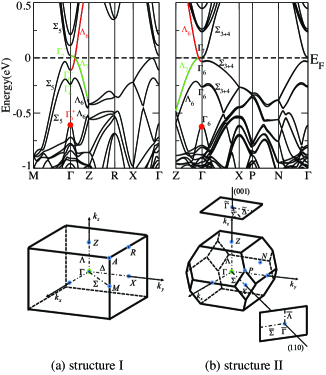
Among the II3-V2-types narrow gap semiconductors, Cd3As2 has drawn crucial attention, because it was believed to have inverted band structure, invert_exp ; invert_theory whereas all others Cd3P2, Zn3As2 and Zn3P2 have normal band ordering. In contrast to other inverted band compounds (like HgTe, HgSe, and -Sn), Cd3As2 belongs to tetragonal symmetry, and is the representative of this group, which has the splitted valence band top at =0. The crystal structure of Cd3As2 is complicated, and can be related to tetragonally-distorted anti-fluorite structure with 1/4 Cd site vacancy. If the distribution of these vacancies is random, one may treat it by virtual crystal approximation (VCA) for simplicity vcafluorite ; vcazb . However, those vacancies are in fact ordered even at room temperature, leading to a tetragonal structure with () symmetry (40 atoms per unit cell, called Structure I hereafter), or a body centered tetragonal structure with () symmetry (80 atoms per unit cell, called Structure II hereafter), with the later structure more favored Cd3As2Struct . This vacancy ordering and very large cell of Cd3As2 cause historically serious problems for theoretical studies, and there is no existing first-principles calculations up to now. We report here the first band structure calculations of Cd3As2 with its true structures and with SOC included.
We perform the first-principles band-structure calculations within the density functional formalism as implemented in VASP vasp , and use the all-electron projector augmented wave (PAW) paw basis sets with the generalized gradient approximation (GGA) of Perdew, Burke and Ernzerhof (PBE) pbe for the exchange correlation potential. The Hamiltonian contains the scalar relativistic corrections, and the spin-orbit coupling is taken into account by the second variation method vsoc . The cutoff energy for the plane wave expansion was 500 eV and a k-point mesh of and are used for the bulk calculations of Structure I and II, respectively.
For the convenience of our later discussions for the effective low energy physics, here we briefly introduce our modified second-order 8-band Kane model ap_kane for typical semiconductors. We start from the standard 4-band second-order Kane model ap_kane for the case of without SOC, and then introduce additional terms to take into account the particular tetragonal symmetry of Cd3As2. In the approximation, considering the low energy , , , states (as basis) around , the modified 4-band Kane model is given as,
comparing with the strandard isotropic 4-band Kane model ap_kane , here we consider the anisotropic tetragonal symmetry, and introduce the paramter for the crystal-field splitting of orbitals. The other parameter is introduced to describe the breaking of inversion symmetry for Structure II, and it should be zero for Structure I. Then our modified 8-band Kane model can be obtained by adding the SOC term as,
where I is the identity matrix and denotes the strength of SOC.
III Results and discussions
III.1 Electronic structures and band inversion

Similar to most of the semiconductors with anti-fluorite or zinc-blende structures, the low energy electronic properties of Cd3As2 are mostly determined by the Cd- states (conduction bands) and the As- states (valence bands), as shown in Fig. 1. However, there are two distinct features: (1) band-inversion around point with the -state (red solid cycle) lower than the -states, which is an important sign of non-trivial topology; (2) semi-metallic with band crossing along the -Z direction. This band-crossing is unavoidable, because the two bands belong to different ( and ) representations respectively, as distinguished by rotational symmetry around axis. The different representation prohibits hybridization between them, resulting in the protected band-crossing. Furthermore, the crossing points should locate exactly at the Fermi level due to charge neutrality requirement, resulting in a 3D Dirac semimetal state with Fermi surface consisting of a single pair of Fermi points (two symmetric points along related by TR). Both the structure I and II share the above common features but with one important difference: structure I has inversion center but structure II doesn’t.
As had been attempted with perturbation method vacant , vacancy ordering and BZ folding play important role for the band-inversion, in contrast to the cases of HgTe or Ag2Te Ag2Te , where it was driven by the the shallow states. To prove this, we performed calculations for Cd3As2 in hypothetic anti-fluorite structure without vacancy (using VCA) and in cubic anti-fluorite structure with one Cd vacancy, keeping the same lattice constant. We found that the former (later) has normal (inverted) band ordering at . At the BZ boundary X point of hypothetic anti-fluorite structure without vacancy, there exist shallow and states, which are folded onto the point of real structure. Therefore, the hybridization among the states with the same representation will push the states away from each other, i.e, make the lowest -state further lower and highest -state higher, resulting in the band inversion at . The band-inversion calculated from GGA is about 0.7 eV for both Structure I and II. Considering the possible underestimation of GGA for the - gap, we have improved the calculations by HSE method hse , and still found the band-inversion around 0.3 eV, being consistent with most of the existing experimental evidence, such as the optical and transport measurements invert_exp .
The calculated band structures of Cd3As2 can be well fitted by using our modified 8-band Kane model presented in previous section, and the obtained parameters are listed in Table.I.
| -0.610367 | -0.069191 | 0.072439 | 0.027 | 0.16 |
| 6.302242 | 8.013873 | -5.675600 | -7.957689 | -10.757965 |
III.2 Minimal Effective Hamiltonian for the 3D Dirac fermion
The atomic Cd- and As- states with SOC can be written as the states with definite angular momentum and , i. e., , , , . In the tetragonal crystal symmetry, however, the total angular momentum is no longer a good quantum number, and the valence -states have complete splitting at . The heavy-hole -state and the conduction -state remain to be the eigenstates at , while the light-hole states can mix with the split-off state , forming two new eigenstates which are irrelevant to the low energy physics here.
The band inversion nature of Cd3As2 around the can be caught by considering only the minimal basis set of , , and states. To describe the 3D Dirac fermion, an effective low energy Hamiltonian can therefore be obtained by downfolding the 8-band model into the subspace spanned by the 4 mimimal basis. The resulting reads,
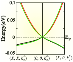
where , , and with parameters , , 0 to reproduce band inversion. Under the tetragonal symmetry, the leading-order term of has to take the high-order form of , which can be neglected if we only consider the expansion up to . The terms containing describe the breaking of inversion symmetry, which should be zero for structure I. In such case, the energy dispersion is , having a pair of four-fold degenerate zero energy Dirac points at =(0, 0, ). Around the neighborhood of each Dirac point, we can further expand the Hamiltonian up to . The resulting Hamiltonian is nothing but the one for 3D massless Dirac fermions, which has anisotropic linear dispersion (where is the deviation of momentum from the Dirac point ). The block diagonal form allows us to decouple the 44 matrix into two 22 matrices, which are Weyl fermions with degenerate energy but opposite chirality. For structure II, which has no inversion symmetry, the non-vanishing D term will modify the in-plane velocity from to , while keep the Weyl nodes degenerate (because the symmetry along the Gamma-Z axis contains only 2D irreducible representations for its double space group). The resulting Dirac semimetal state has 4-fold degenerate Dirac points, but with splitting of in-plane band dispersions away from Dirac points (Fig. 2). This is a new type of 3D Dirac semimetal state, in contrast to other examples BiO2 ; Na3Bi .

A stable Weyl semimetal state with two Weyl nodes separated in momentum space can be introduced either by lowering the crystal symmetry from to , or by breaking the TR symmetry Na3Bi . In particular, due to the large -factor (around 3040) of Cd3As2 g-factor , an exchange-splitting of 2meV can be introduced by moderate 1T magnetic field (if we neglect the orbital effects). On the other hand, if the 4-fold rotational symmetry is broken, a linear leading order term of , will be introduced in the effective Hamiltonian . In such case, two Weyl nodes will be coupled together, resulting in a massive Dirac fermions with gap opening. We have checked the topological invariant number for this resulting insulating state, and found it is odd, confirming that it is a 3D topological insulator TIreview ; TIreview-2 (due to the inverted band structure).
III.3 Surface states and quantum transport properties
The non-trivial topology and the 3D Dirac cones in Cd3As2 suggest the presence of non-trivial surface states. For this purpose, we transform the eight-band model into a tight-binding model on a tetragonal lattice by introducing the substitutions:
Here, refers to , and , while and are the tetragonal lattice constants, which are taken as 3.0 Å and 5.0 Å, respectively. This approximation is valid in the vicinity of the point. We use an iterative method to obtain the surface Green’s function of the semi-infinite system zhangw . The imaginary part of the surface Green’s function is the local density of states (LDOS) at the surface. Since GGA underestimate the - band gap by about 0.4 eV as discussed above, we have artificially lifted the on-site energy of -state (as given in Table. 1) by 0.4 eV in the surface state calculations.
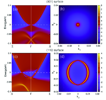
The obtained LDOS on semi-infinite (001) and (110) surfaces of the structure II are presented in Fig. 3. For (001) surface, the surface projection of continuous bulk states superposes the non-trivial surface states, and its Fermi surface is just a point (Fig. 3(b)). For (110) surface, however, the non-trivial surface states are clearly visible. Its Fermi surface is composed of two half-circle Fermi arcs, touching at the singularity points (, ) where the surface projection of bulk Dirac points exist.

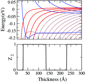
The existence of 3D Dirac cones in the bulk also implies that we can expect the QSH effect if we reduce the dimensionality and form the quantum well structure of Cd3As2. This provides an alternative compound choice to the existing experiments expHgTe ; typeII , which all require extreme conditions up to now. The band structure of -oriented Cd3As2 thin film of different thickness can be understood as the bulk bands in different -fixed planes. The 2D Z2 number can be nonzero only for limited regions where the band inversion happens when going from to Z. In the quantum-well structure, those low energy states around should be further quantized into subbands, whose energy levels change as a function of film thickness (Fig. 4(a)). When the thickness of the film is thin enough, the band inversion in the bulk band structure will be removed entirely by the finite size effect. With the increment of the film thickness, finite size effect is getting weaker and the band inversion among these subbands restores subsequently, which leads to jumps in the Z2 number. Then, depending on the number of band inversions associated with the sub-bands, the system should cross over between trivial and nontrivial 2D insulators oscillatorily as a function of thickness oscillatory (Fig. 4(b)). Comparing with HgTe/CdTe quantum well expHgTe , the first critical thickness of Cd3As2 is much thinner (2.9nm vs. 6.3nm), suggesting possibly larger gap. To be a concrete example, 5nm thick Cd3As2 film is a good QSH insulator with gap more than 100meV. Given the known high mobility of Cd3As2, it is therefore a good candidate for the QSH measurement.

Finally we propose that crystalline Cd3As2 with 3D Dirac cone is an ideal system to check Abrikosov’s proposal of quantum MR MR , and may support sizable linear MR even up to room temperature. Quantum effects become noticeable when the individual Landau levels are distinct: . Dirac system has linear energy spectrum, and its cyclotron frequency should follow the square root rule (=), in contrast with non-relativistic system where is linear in field . Using calculated velocity =cm/s for Cd3As2, this then leads to 280K for =10T. The linear quantum MR can be estimated MR as == (where =1/ is used, is carrier density, is mobility, and is the density of scattering centers). Taking the experimental values 1.5m2V-1s-1 at room temperature, and assuming and are in the same order, MR ratio can reach 50% per 1T field. If the scattering is not phonon-mediated, we expect that is not sensitive to temperature, then MR is mostly determined by and , which should lead to even enhanced MR at lower temperature.
IV Conclusion
In summary, based on the first-principles calculations and effective model analysis, we have shown that the known compound Cd3As2 is a symmetry-protected topological semimetal with a pair of 3D Dirac points (located at the Fermi level) in the bulk and Fermi arcs on the surfaces. It can be driven into various topologically distinct phases, such as topological insulator and Weyl semimetal state by symmetry breakings. In addition, due to its unique 3D Dirac cone type electronic structure, we can expect the QSH effect in its quantum well structure and the sizable linear quantum MR even up to the room temperature. It will be of particular interest, in such a 3D topological semimetal, to see whether the superconductivity can be achived by carrier doping or not, because such superconducting state if obtained may be related to the topological superconductivity TSC .
Acknowledgements.
The first-principles calculations are performed by using the computers in the Nation Supercomputer Center in Tianjin of China. We acknowledge the supports from NSF of China, the 973 program of China (No. 2011CBA00108 and 2013CBP21700).References
- (1) H. Weyl, Z. Phys. 56, 330 (1929).
- (2) G. T. Volovik, JETP Lett. 75, 55 (2002).
- (3) Z. Fang, N. Nagaosa, K. S. Takahashi, and et.al., Science 302, 92 (2003).
- (4) X. G. Wan, A. M. Turner, A. Vishwanath, S. Y. Savrasov, Phys. Rev. B 83, 205101 (2011).
- (5) G. Xu, H. M. Weng, Z. J. Wang, X. Dai, Z. Fang, Phys. Rev. Lett. 107, 186806 (2011).
- (6) A. A. Burkov, L. Balents, Phys. Rev. Lett. 107, 127205 (2011); A. A. Burkov, M. D. Hook, L. Balents, Phys. Rev. B 84, 235126 (2011); G. B. Halász, L. Balents, Phys. Rev. B 85, 035103 (2012).
- (7) M. Z. Hasan, and C. L. Kane, Rev. Mod. Phys. 82, 3045 (2010).
- (8) X.-L. Qi, and S.-C. Zhang, Rev. Mod. Phys. 83, 1057 (2011).
- (9) H. J. Zhang, et.al., Nature Phys. 5, 438 (2009); Y. Xia, et.al., Nature Phys. 5, 398 (2009); Y. L. Chen, et.al., Science 325, 178 (2009).
- (10) S. M. Young, S. Zaheer, J. C. Y. Teo, C. L. Kane, E. J. Mele, and A. M. Rappe, Phys. Rev. Lett. 108, 140405 (2012).
- (11) J. L. Mañes, Phys. Rev. B 85, 155118 (2012).
- (12) Z. J. Wang, Y. Sun, X. Q. Chen, C. Franchini, G. Xu, H. M. Weng, X. Dai, and Z. Fang, Phys. Rev. B 85, 195320 (2012).
- (13) S. Murakami, New J. Phys. 9, 356 (2007).
- (14) See, W. Zdanowicz, and L. Zdanowicz, Ann. Rev. Mater. Sci. 5, 301 (1975), and references therein.
- (15) M. J. Aubin, L. G. Caron, and J.-P. Jay-Gerin, Phys. Rev. B 15, 3872 (1977); L. G. Caron, J.-P. Jay-Gerin, and M. J. Aubin, Phys. Rev. B 15, 3879 (1977).
- (16) B. Dowgiallo-Plenkiewicz, P. Plenkiewicz, Phys. Stat. Sol. (b) 94, K57 (1979); G. Chuiko, N. Don, et al, Moldavian Journal of the Physical Sciences 2 N1.88 (2003).
- (17) P. J. Lin-Chung, Phys. Rev. 188, 1272 (1969).
- (18) K. Sieranski, J. Szatkowski, and J. Misiewicz, Phys. Rev. B 50, 7331 (1994).
- (19) G.A. Steigmann and J. Goodyear, Acta Cryst. B24, 1062 (1968).
- (20) G. Kresse and J. Hafner, Phys. Rev. B 48, 13115 (1993); G. Kresse and J. Furthmüller, Comput. Mater. Sci. 6, 15 (1993)
- (21) P. E. Blöchl, Phys. Rev. B , 17953 (1994); G. Kresse and D. Joubert, Phys. Rev. B , 1758 (1999)
- (22) J. P. Perdew, K. Burke and M. Ernzerhof, Phys. Rev. Lett. , 3865 (1996)
- (23) D. D. Koelling and B. N. Harmon, J. Phys. C: Solid State Phys. , 3107 (1977)
- (24) Lok C. Lew Yan Voon and M. Willatzen, The kp Method: Electronic Properties of Semiconductors (Springer, Berlin, 2009). See pp. 59-60 for the definition of parameters and Four-bands Kane model.
- (25) B. Plenkiewicz, P. R. Wallace and P. Plenkiewicz, Solid State Comm. 50, 681 (1984).
- (26) W. Zhang, R. Yu, W. Feng, Y. Yao, H. M. Weng, X. Dai, Z. Fang, Phys. Rev. Lett. 106, 156808 (2011).
- (27) J. Heyd, G. Scuseria, and M. Ernzerhof, J. Chem. Phys.118, 8207 (2003).
- (28) J. Bodnar, Proc. 3rd Inter. Conf. Phys. of Narrow-gap Semicond., PWN Warsaw (1977); P. R. Wallace, Phys. Status Solidi (b) 92, 49 (1979).
- (29) W. Zhang, R. Yu, H. J. Zhang, X. Dai, and Z. Fang, New J. Phys. 12, 065013 (2010).
- (30) M. Kónig, S. Wiedmann, C. Brune, A. Roth, H. Buhmann, L. W. Molenkamp, X.-L. Qi, S.-C. Zhang, Science 318, 766 (2007).
- (31) C. X. Liu, T. L. Hughes, X. L. Qi, K. Wang, S.-C. Zhang, Phys. Rev. Lett. 100, 236601 (2008); I. Knez, R. R. Du, and G. Sullivan, Phys. Rev. Lett. 107, 136603 (2011).
- (32) C. X. Liu, H. J. Zhang, B. H. Yan, X. L. Qi, T. Frauenheim, X. Dai, Z. Fang, and S. C. Zhang, Phys. Rev. B 81, 041307 (2010).
- (33) A. A. Abrikosov, Phsy. Rev. B 58, 2788 (1998).
- (34) X. L. Qi, T. L Hughes, S. C. Zhang, Phys. Rev. B 81, 134508 (2010).