Intrinsic and extrinsic origins of low-frequency noise in GaAs/AlGaAs Schottky-gated nanostructures
Abstract
We study low-frequency noise in current passing through quantum point contacts fabricated from several GaAs/AlGaAs heterostructures with different layer structures and fabrication processes. In contrast to previous reports, there is no gate-dependent random telegraph noise (RTN) originating from tunneling through a Schottky barrier in devices fabricated using the standard low-damage process. Gate-dependent RTN appears only in devices fabricated with a high-damage process that induces charge trap sites. We show that the insertion of AlAs/GaAs superlattices in the AlGaAs barrier helps to suppress trap formation. Our results enable the fabrication of damage-resistant and thus low-noise devices.
Low-frequency noise in the source-drain resistance of metal-oxide-semiconductor and GaAs high-electron-mobility transistors arising from background charge fluctuations have been a long-standing issue [1-3]. As the device size decreases, device properties become increasingly susceptible to local charge fluctuations. The noise can exhibit either or random telegraphic behavior depending on the number of charge trap sites involved [4]. In mesoscopic or nanoscale devices such as quantum point contacts (QPCs) and quantum dots (QDs), single electron hopping occurring at somewhat distant sites can be resolved as a measurable change in the device characteristics. Because of their high charge sensitivity, QPCs have been widely used as charge sensors for detecting individual charges in QDs, which constitutes a key element of the present quantum information technology based on QDs. However, the precision of the state readout is limited by the conductance fluctuation of the QPC arising from uncontrolled background charge motion. Background charge noise also causes fluctuations of the energy levels in QDs, which results in decoherence and gate error in both charge [5-7] and spin qubits [8-10].
Several mechanisms have been considered as the origin of the low-frequency noise in GaAs-based devices, including electron hopping between the two-dimensional electron gas (2DEG) and trap sites [11, 12], current leakage through the Schottky barrier [13-16], and electron hopping within the remote-doping layer [17, 18]. An important observation in these studies is that the low-frequency charge noise increases as the voltage applied to the surface Schottky gate is decreased and becomes more negative. Since the Schottky barrier becomes less opaque with decreasing , the observed dependence was interpreted as evidence that the current leakage through the Schottky barrier was responsible for the charge noise. The strong dependence of the noise, in turn, allowed the reduction of the charge noise by employing bias cooling [14] or an additional global top gate [15], both of which shift the operation point to a less negative voltage. In an attempt to eliminate the charge noise associated with doping, single-electron transistors based on undoped structures have been fabricated [19]; however, the anticipated noise reduction has not yet been demonstrated.
In this paper, we study the effects of the layer structure and fabrication process on the low-frequency current noise in QPC devices fabricated from GaAs/Al0.3Ga0.7As modulation-doped heterostructures at 4.2 K to clarify the origin of the noise. Specifically, in addition to the standard delta-doped structure, we examined a structure in which AlAs/GaAs superlattice (SL) barriers are inserted above and below the delta-doping layer—if the current leakage through the Schottky barrier is the prime contributor to the charge noise, the noise should be suppressed by employing the SL barriers, as suggested in Ref. 15. As opposed to previous reports [14, 15] and the above expectation, we found the noise in our devices to be nearly independent and unaffected by the SL barriers. On the other hand, devices fabricated using a high-damage process that induces charge trap sites exhibited strongly -dependent noise characterized by random telegraphic behavior. We show that the inclusion of SL barriers helps to suppress the formation of trap sites and, accordingly, reduce the process-induced -dependent noise. Our results pave the way to obtaining stable gated nanostructures without bias cooling or a global top gate and assist in the fabrication of damage-resistant devices.
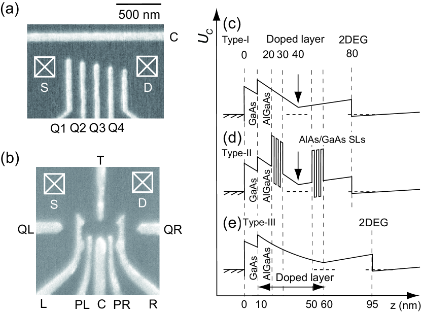
We examined the use of devices with QPC and double quantum dot (DQD) gate layouts, as shown in Fig. 1(a) and (b), respectively, to measure the charge noise. A QPC device is defined by applying the same gate voltage to the center gate C and one of the finger gates Qi (-). The gap between C and Qi ranges from to nm (in 30-nm steps), which allows the in-situ comparison of QPCs with different operation gate voltages. For the DQD-type devices, a QPC was formed by applying the same to two of eight gates, where the operation voltage was varied by activating a different gate pair. We examined three kinds of layer structures with conduction band profiles as schematically shown in Fig. 1(c)-(e). Type-I is a standard delta-doped structure [Fig. 1(c)]. In type-II, 10-nm-thick AlAs/GaAs (2.1 nm/0.56 nm) SL barriers are inserted above and below the delta-doping layer [Fig. 1(d)]. A uniform-doped structure (type-III) was also examined [Fig. 1(e)].
The samples we investigated and the wafers we used are listed in Table I together with their properties. In addition to the standard process that we use to fabricate QPC and DQD devices, we also examined the effects of a high-damage process by additionally employing intense UV ozone cleaning at C for 3 minutes prior to the electron-beam lithography. While this eliminates the remaining photoresist and facilitates the lift-off process, it also induces considerable damage, as evidenced by the decrease in the carrier density and the mobility (sample E, Table I). For the structure with the SL barriers, the same process had much less effect on the carrier density and the mobility (sample F, Table I), which we discuss later. All measurements were performed at 4.2 K. Unless otherwise noted, the results presented below were obtained from devices fabricated with the standard process.
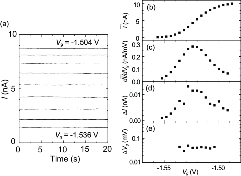
Figure 2(a) shows a typical measurement for sample A. We applied a source-drain voltage of 300 V and measured the current through the QPC over 20 seconds at several values with the QPC conductance below the first plateau, i.e., , where is an elementary charge and is Planck’s constant. Following the method in Ref. [20], we characterize the charge noise in terms of the equivalent gate voltage noise defined as , where and are the time average and fluctuation of . Here, [Fig. 2(d)] was calculated as
using the Fourier power spectrum of , and and [Fig. 2(b) and (c)] were calculated numerically from the data [21]. As shown in Fig. 2(d), clearly depends on , which precludes the noise from the current amplifier as the origin of the observed noise. We note that the voltage noise on the gates is also negligible, as the resolution ( ) of the voltage sources that we employed is about one order of magnitude smaller than the measured [Fig. 2(e)]. As shown in Fig. 2(e), is not greatly influenced by a change in with , and remains nearly constant over the range .
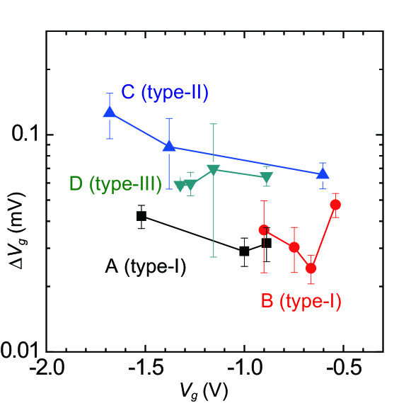
Figure 3 shows measured for QPCs fabricated from four different wafers as a function of operating point . Each data point corresponds to a different gate combination, representing an average taken over several values near the corresponding central operation voltage. The error bars indicate the standard deviation. We first note that, in the standard delta-doped structure (type-I), the measured noise is only weakly dependent on . This also indicates that the measured noise level appropriately reflects the property of the sample and does not depend on the position or specific configuration of the QPC. Such -independent noise is in sharp contrast to that described in Ref. 15, where increased exponentially as was decreased below V. As demonstrated in Refs. 14 and 15, increases because decreasing makes the Schottky barrier less opaque and thus enhances the tunneling probability from the gate to the trap sites in the AlGaAs barrier. The absence of such strong dependence in our devices suggests that tunneling through the Schottky barrier is irrelevant to the observed noise. This conjecture is also supported by a comparison of the noise levels of our devices and those studied in Ref. 15. Whereas at a small negative the noise levels in samples A and B are twice that reported in Ref. 15, due to the absence of dependence, these devices exhibit much less noise at a large negative . This enables us to define stable nanostructures such as a QPC or a QD without employing bias cooling or an additional global gate; this is a strong advantage, because it lifts the restrictions on the operation voltage set by bias cooling or a global gate, thereby greatly enhancing the degree of freedom in tailoring desired nanostructures.
As shown in Fig. 3, the insertion of the SL barriers did not reduce the noise level in our devices (type-II). The independence of the charge noise as regards the presence or absence of the SL barriers lends support to the above conjecture that tunneling through the Schottky barrier is irrelevant to the noise observed in our devices. The behavior of the sample fabricated from the uniform-doped structure (type-III) is similar to that of the other samples.
Another important feature of our data is that it is free from random telegraphic, or switching behavior, even for large negative values, as seen in Fig. 2(a). Indeed, we observed no switching noise, or random telegraphic noise (RTN) for measurements obtained over a number of hours. This was true for all the devices that we examined that were fabricated with the standard process, independent of the type of layer structure or doping. Note that RTN appears when only a few trap sites located near the QPC are the prime contributors to the charge fluctuation. The absence of RTN in our devices, combined with the low noise level at a large negative , implies that in our devices there is no trap site available for tunneling electrons near the QPC. This also suggests that switching noise due to tunneling through a Schottky barrier is not necessarily inherent to GaAs-based modulation-doped structures.
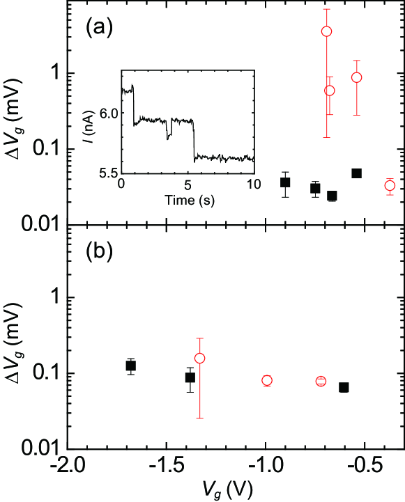
The absence of RTN in our devices in turn suggests the existence of extrinsic origins of RTN. To explore this possibility, we examined the effects of process-induced charge traps by additionally employing intense UV ozone cleaning prior to the electron-beam lithography. This process induces charge trap sites, as evidenced by the significant decrease in the mobility (sample E, Table I). As shown in the inset to Fig. 4(a), we did observe RTN in the device fabricated with the intense UV cleaning. In Fig. 4(a), we plot of this device as a function of and compare it with the results obtained for a device fabricated from the same wafer using the standard process. The intense UV cleaning induced strongly -dependent noise that increased rapidly below V, which confirms the link between strong dependence and random telegraphic behavior.
Interestingly, we found that the SL barriers played an unexpected role that would allow us to make devices much more resistant to damage from processing. As shown in Table I, the inclusion of SL barriers (sample F) attenuates the deleterious effect that processing has on carrier density and mobility. This is particularly clear for the mobility, which differs by almost one order of magnitude. This result clearly shows that the SL barriers help to suppress the formation of trap sites. The reduced trap density is also evident in the noise behavior. In contrast to the results for the samples without SL barriers, is barely affected by the high-damage process and remains almost independent as shown in Fig. 4(b). It is possible that the SL barriers block tunneling through the Schottky barrier and thereby suppress the -dependent RTN. In the present case, however, it is more likely that the reduced RTN is due to the lower trap density, as clearly demonstrated by the electron density and the mobility (Table I). Although the exact mechanism for the suppressed trap formation is unknown, our finding enables the fabrication of damage-resistant and thus low-noise devices.
Finally, we discuss the origin of the -independent noise observed in the samples fabricated with the standard low-damage process. In the samples fabricated with the high-damage process, the spatial range over which the trap sites relevant to the RTN are distributed can be crudely estimated from the size of the current step at each switching event. In our DQD-type devices, the operating voltage of the QPC charge sensor shifts by 1.3 (0.9) mV (data not shown) when one electron is added to or removed from the QD on the near (far) side about 300 (400) nm from the QPC. Since the observed RTN corresponds to a shift in the QPC operating voltage a few times larger than these values, we can estimate that the relevant trap sites are distributed within nm of the QPC. This estimate, which also implies that the relevant trap sites are located close to the split gate, is consistent with the noise being strongly dependent. In turn, it follows that the -independent noise dominant in our devices fabricated with the standard process is due to charge hopping taking place at distant sites distributed over a much wider spatial range. This picture is consistent with the absence of switching behavior and dependence. As we discussed above, vertical tunneling through the AlGaAs (or SL) barrier is unlikely to be its origin. We therefore speculate that charge hopping within the remote-doping layer is the most likely cause of the -independent noise. However, we do not know why the noise level differs among wafers with the identical doping (compare samples A, B, and C in Fig. 3, which all have the same doping level). Indeed, even though device E has high charge trap density, it shows lower noise than sample F at V, where RTN is absent (Fig. 4). This result may be attributed to the difference in the starting material. If so, it implies that these process-induced traps do not contribute to the -independent noise. A further investigation is necessary to clarify the origin of the -independent noise.
In summary, we identified two types of low-frequency noise in GaAs/AlGaAs QPCs distinguished by dependence linked with the presence/absence of switching behavior. Our results indicate that the commonly observed -dependent switching noise is not necessarily an intrinsic property of modulation-doped GaAs/AlGaAs heterostructures and point to the importance of eliminating extrinsic origins of low-frequency noise. We found that the inclusion of SL barriers attenuates damage from processing that can be a source of low-frequency noise. Our findings will thus enhance the degree of freedom in tailoring low-noise Schottky-gated nanostructures and assist in the fabrication of devices that are resistant to damage from processing.
Part of this work was supported financially by the MEXT Grant-in-Aid for Scientific Research on Innovative Areas (21102003), and the Funding Program for World-Leading Innovative R&D on Science and Technology (FIRST).
[1] M. J. Kirton and M. J. Uren, Advances in Physics, 38, 367 (1989).
[2] Y. P. Li, D. C. Tsui, J. J. Heremans, and J. A. Simmons, Appl. Phys. Lett. 57, 774 (1990).
[3] D. H. Cobden, N. K. Patel, M. Pepper, D. A. Ritchie, J. E. F. Frost, and G. A. C. Jones, Phys. Rev. B 44, 1938 (1991).
[4] S. Machlup, J. Appl. Phys. 25, 341 (1954).
[5] T. Hayashi, T. Fujisawa, H. D. Cheong, Y. H. Jeong, and Y. Hirayama, Phys. Rev. Lett. 91, 226804 (2003).
[6] K. D. Petersson, J. R. Petta, H. Liu, and A. C. Gossard, Phys. Rev. Lett. 105, 246804 (2010).
[7] T. Itakura and Y. Tokura, Phys. Rev. B 67, 195320 (2003).
[8] J. R. Petta, A. C. Johnson, J. M. Taylor, E. A. Laird, A. Yacoby, M. D. Lukin, C. M. Marcus, M. P. Hanson, and A. C. Gossard, Science 309, 2180 (2005).
[9] Q. Li, L. Cywinski, D. Culcer, X. Hu, and S. Das Sarma, Phys. Rev. B 81, 085313 (2010).
[10] D. Culcer, X. Hu, and S. Das Sarma, Appl. Phys. Lett. 95, 073102 (2009).
[11] C. Dekker, A. J. Scholten, F. Liefrink, R. Eppenga, H. van Houten, and C. T. Foxon, Phys. Rev. Lett. 66, 2148 (1991).
[12] T. Sakamoto, Y. Nakamura, and K. Nakamura, Appl. Phys. Lett. 67, 2220 (1995).
[13] D. H. Cobden, A. Savchenko, M. Pepper, N. K. Patel, D. A. Ritchie, J. E. F. Frost, and G. A. C. Jones, Phys. Rev. Lett. 69, 502 (1992).
[14] M. Pioro-Ladriere, J. H. Davies, A. R. Long, A. S. Sachrajda, L. Gaudreau, P. Zawadzki, J. Lapointe, J. Gupta, Z. Wasilewski, and S. Studenikin, Phys. Rev. B 72, 115331 (2005).
[15] C. Buizert, F. H. L. Koppens, M. Pioro-Ladriere, H-P. Tranitz, I. T. Vink, S. Tarucha, W. Wegscheider, and L. M. K. Vandersypen, Phys. Rev. Lett. 101, 226603 (2008).
[16] Y. X. Liang, Q. Dong, M. C. Cheng, U. Gennser, A. Cavanna, and Y. Jin, Appl. Phys. Lett. 99, 113505 (2011).
[17] G. Timp, R. E. Behringer, and J. E. Cunningham, Phys. Rev. B 42, 9259 (1990).
[18] C. Kurdak, C. J. Chen, D. C. Tsui, S. Parihar, S. Lyon, and G. W. Weimann, Phys. Rev. B 56, 9813 (1997).
[19] A. M. See, O. Klochan, A. R. Hamilton, A. P. Micolich, M. Aagesen, and P. E. Lindelof, Appl. Phys. Lett. 96, 112104 (2010).
[20] S. W. Jung, T. Fujisawa, Y. Hirayama, and Y. H. Jeong, Appl. Phys. Lett. 85, 768 (2004).
[21] We have confirmed that the high-frequency components above 25 Hz have a negligible contribution to .
| sample | wafer # | wafer structure | fabrication process | gate layout | ||
|---|---|---|---|---|---|---|
| A | R193 | type-I | standard | 2.3 | 1.8 | DQD |
| B | R244 | type-I | standard | 2.2 | 1.3 | QPC |
| C | R219 | type-II | standard | 2.3 | 1.3 | DQD |
| D | R247 | type-III | standard | 2.5 | 2.9 | QPC |
| E | R244 | type-I | high-damage | 1.9 | 0.14 | QPC |
| F | R219 | type-II | high-damage | 2.3 | 1.2 | DQD |