Band nesting and the optical response of two-dimensional semiconducting transition metal dichalcogenides
Abstract
We have studied the optical conductivity of two-dimensional (2D) semiconducting transition metal dichalcogenides (STMDC) using ab initio density functional theory (DFT). We find that this class of materials presents large optical response due to the phenomenon of band nesting. The tendency towards band nesting is enhanced by the presence of van Hove singularities in the bandstructure of these materials. Given that 2D crystals are atomically thin and naturally transparent, our results show that it is possible to have strong photon-electron interactions even in 2D.
pacs:
71.20.Mq,78.40.Fy,71.10.-wSemiconductor transition metal dichalcogenides (STMDC) are a family of crystals with a chemical formula MX2 where M = W, Mo, Ti, Zr, Hf, Pd, Pt, and others, and X = S, Se, Te,wilson_charge-density_1975 ; wang_electronics_2012 ; chhowalla_chemistry_2013 which can exist in a two-dimensional (2D) structure consisting of one layer of transition metal atoms sandwiched by two layers of chalcogens, all in hexagonal sublattices. They have two known structural polytypes, trigonal prismatic (T) and octahedral (O), which can be distinguished by the relative stacking of the chalcogenide layers. Most 2D STMDC have band gaps in the visible range, between 1 eV and 3 eV, and have been the subject of study in the last few yearsfuhrer2012 ; Mak2010 since the emergence of the field of 2D crystals.neto_new_2011 Because of these band gaps, in a technologically interesting range, these materials are being considered for a new generation of 2D transistor, sensor, and photovoltaic applications.
It was discovered recently Britnell2013 that these materials have strong optical properties even when they are only three atoms thin. This is rather surprising because atomically thin films like these, only tens of Ångströms in thickness, are naturally transparent and we would not expect a strong photon-electron coupling a priori. In this article, we show that this extraordinary optical response is due to the phenomenon of “band nesting", namely, the fact that in the bandstructure of these materials there are regions where conduction and valence bands are parallel to each other in energy. Band nesting implies that when the material absorbs a photon, the produced electrons and holes propagate with exactly the same, but opposite, velocities. We find that band nesting is present in the bandstructure of all these materials. Furthermore, the existence of strong van Hove singularities (VHS) facilitates the phenomenon of band nesting. In two-dimensional materials, the band-nesting results in a divergence of the joint density of states, leading to very high optical conductivity. We present calculations of the optical response of the 2D STMDC with S,Se, illustrating how it is enhanced by the phenomenon of band nesting.
.1 Band nesting
In semiconductors, the band gap plays an important role in what concerns optical absorption. It defines the threshold after which there is absorption of electromagnetic radiation, by the promotion of an electron from the valence band to the conduction band. But the largest absorption is usually not at the band gap edge; it is often considered to be in a VHS in the electronic structure. These correspond to singularities in the density of states; if at a given point of the reciprocal space there are VHS both in the conduction and the valence band, there will be a singularity of the optical conductivity. Yet, this coincidence normally happens only at high symmetry points, and there are very few in the Brillouin Zone (BZ). A particular case is the extended van Hove singularity (EVHS) in that these are single band saddle points with a flat band in one of the directions.gofron_observation_1994
The optical conductivity of a material can be written as
where is the imaginary part of the relative electric permittivity, is the frequency of the incoming electromagnetic radiation, and is the vacuum permittivity. In the optical dipole approximation we can write:
| (1) |
The sum is over the occupied states in the valence band () and the unoccupied states in the conduction band () with energies and , and includes implicitly the sum over spins, ( is the electric charge and the carrier mass), is the dipole matrix element. The integral in (1) is evaluated over the entire 2D BZ. If we consider cuts of constant energy , , in the bandstructure, we can write:
and the integral in (1) can be rewritten as:
Notice that the strong peaks in the optical conductivity will come from regions in the spectrum where . If varies slowly over these regions (so that there is a gradient expansion) we can write:
where
is the joint density of states (JDOS).
The points where are called critical points (CP) and they can be of several types. If we have either a maximum, a minimum or a saddle point in each band; this usually occurs only at high symmetry points. These points often receive more attention, because they are easy to pinpoint by visual inspection of the bandstructure, and give rise to singularities in the DOS. On the other hand, the condition with , that is band nesting, gives rise to singularities of the JDOS, and therefore to high optical conductivity. Notice that this condition differs from an EVHS gofron_observation_1994 in that the later refers to saddle points in one band, with a flat band in one of the directions, while here it is determined by the “topographic” difference between the conduction and valence bands. In the case of two dimensional materials, a saddle point of gives rise to a divergence of the optical conductivity, whereas in 3D materials it merely gives rise to an edge with dependence, in first approximation.bassani-book
I Method
We performed a series of DFT calculations for the STMDC family using the open source code Quantum ESPRESSO.Giannozzi2009 We used norm conserving, fully relativistic pseudopotentials with nonlinear core-correction and spin-orbit information to describe the ion cores.PSEUDO The exchange correlation energy was described by the generalized gradient approximation (GGA), in the scheme proposed by Perdew, Burke and ErnzerhofPerdew1996 (PBE). The integrations over the Brillouin-zone (BZ) were performed using scheme proposed by Monkhorst-PackMonkhorst1968 ; dft for all calculations except those of the density of states, for which the tetrahedron methodBlochl1994 was used instead. We calculated the optical conductivity directly from the bandstructure.epsFR It is well known that GGA underestimates the band gap,komsa-PRB-86-241201 and hence the optical conductivity shows the peaks displaced towards lower energies relative to actual experiments. However, their shapes and intensities are expected to be correct.
We notice the importance of including spin-orbit and so to perform full relativistic, non-collinear calculations zhu_giant_2011 ; ramasubramaniam_tunable_2011 . Significant spin-orbit splittings in the range 50 meV to 530 meV can be obtained in these crystals and can be measured using current spectroscopic techniques. Still, spin-orbit interaction is ignored in most of DFT calculations ataca_stable_2012 ; bhattacharyya_semiconductor-metal_2012 ; ding_first_2011 ; kuc_influence_2011 . In our case, even for light transition metals, such as Ti, we can have a spin-orbit splitting of the order of 40 meV, which can be easily measured. The trigonal prismatic (T) geometry does not have inversion symmetry, and has a considerable spin-orbit splitting, specially around the high symmetry point K. The octahedral structure (O) has inversion symmetry, and therefore no spin-orbit splitting can be observed (). This results from the inversion symmetry of the energy bands in the reciprocal space, which implies that and , while time reversal symmetry (preservation of the Kramers degeneracy) requires that .
II Results
II.1 Bandstructure calculations
Calculations of the electronic structure were performed for all 2D with S, Se, for both the trigonal prismatic and octahedral structures. Amongst these, we found eleven to be semiconductors. Unless otherwise stated, we will only show results for the lowest energy structures for each compound, which are the T structure for Mo and W and the O structure for Ti, Zr, Pt and Pd. However, the same analysis can be extended to the metastable structures as well.
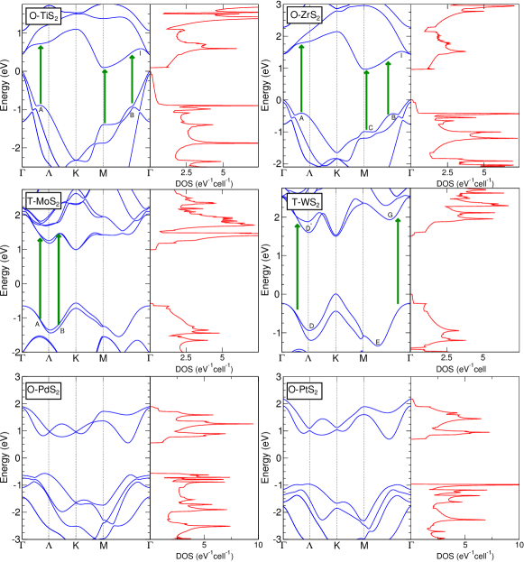
The electronic bandstructures and density of states (DOS) of TiS2, ZrS2, MoS2, WS2, PtS2 and PdS2 are shown in Fig. 1. It is useful to compare the results for dichalcogenides with belonging to the same group of the periodic table, which usually have the same lowest energy structure type and have similar features in the bandstructure close to the gap. The same can be said of S2 and Se2 for the same transition metal. However, T and O structures, even of the same material, are very different. Nevertheless, all of them present Van Hove singularities of , or both, including saddle points which give rise to sharp peaks in the DOS.
We start by analyzing the bandstructure of WS2, one of the most studied STMDC. At the K point, where the direct gap is smallest, the Van Hove singularities are the minimum of and maximum of , and therefore only give rise to steps of the DOS. These steps are low compared to the sharp peaks originating on the very flat bands near the conduction band minimum between the M and the points (see point marked as G in Fig. 1), which is not a high symmetry point. Still, the singularity of the DOS itself is not sufficient to explain the high absorption peak that can be seen in the optical conductivity (see Fig. 2).
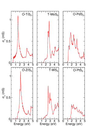
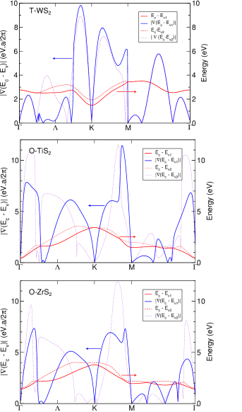
In order to identify the origin of the largest peak at low energy (at 2.56 eV), we analyze the energy difference between the lowest unoccupied band and the highest occupied band, (the index of will be omitted for simplicity), together with its gradient, along the high symmetry lines of the Brillouin Zone (Fig. 3). We find the gradient to be very low between the and the points (corresponding to transitions signaled in Fig. 1) which is the first large optical conductivity peak at 2.56 eV. It is also small near the right arrow of Fig. 1, at around 2.7 eV. We define the regions where this band nesting occurs using the criteria eV/() (where is the modulus of the reciprocal lattice vector).
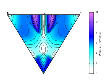
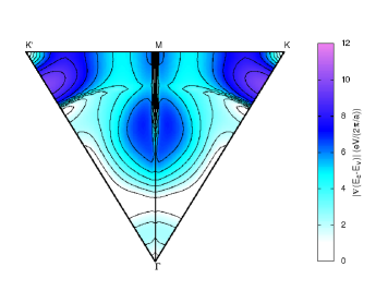
We explored all the BZ to find the extent of the band nesting. Figure 5 shows for WS2. The large white areas close to are the areas where band nesting occurs for these two bands.
The band nesting can also be observed for other bands immediately below or above, as for example for the transitions between the second highest band and the conduction band (), also illustrated in Fig. 1. For example the 2.96 eV peak in optical conductivity results mostly from contributions of other bands.
The bandstructures of the other trigonal prismatic compounds, WSe2, MoS2 and MoSe2 display similar band nesting.
The band nesting is also present in the bandstructure of octahedral polytype compounds. Figure 1 shows the bandstructure and DOS of O-TiS2 single layer. This material exists in the bulk in the octahedral form, and was predicted to be an energetically stable semi-metal ataca_stable_2012 . However, our calculations show it to be an indirect band gap semiconductor, with a small gap. Experimentally, the bulk form of TiS2 is a very narrow band gap semiconductorkukkonen_transport_1981 ; chen_angle-resolved_1980 ( eV). This value is probably underestimated due to the semilocal approximation used for the exchange and correlation energy functional. We also note that, since there is no spin-orbit splitting, all the bands shown are degenerate, and so contribute doubly to the DOS.
Following the same reasoning we used for the trigonal prismatic materials and analyzing the energy gradients (Fig. 3), we notice that eV/() in the regions corresponding to the arrows of Fig. 1. There is another band bellow, and very close in energy to the highest occupied band, which is also plotted in Fig. 1. Since it has transition energies very close to the ones from the highest occupied band, it mostly reinforces the peaks due to the band nesting. All the three transitions have similar energies, being the strongest near M at 1.5 eV; the others contribute to the large broadening of the peak in the optical conductivity (Fig. 2).
We analyze the extent of this band nesting over the BZ by plotting for TiS2 (Figure 4). In white we have the zone corresponding to values less than 1 eV/(). It can be seen that band nesting extends significantly beyond the high symmetry lines. The larger the area, the more intense the absorption peak is expected to be.
Another element of this family, ZrS2, behaves in a similar way. ZrS2 has the same octahedral structure and the same number of valence electrons as TiS2. But in this case, the gap is much wider (Fig. 1).
The transitions marked by the arrows in Fig. 1 correspond to regions where the gradient of is small (Fig. 3). Hence, the absorption is very high at these energies, as can be seen in Fig. 2. There we have two very close peaks, forming a very broad peak. They correspond to a transition at the M point with an energy eV, and the transition indicated by the letter A with an energy eV. The transitions at B ( eV) also give some contribution to the broadening of the peak in the optical conductivity. The transition at M is even stronger than for TiS2. Both TiS2 and ZrS2 have absorption at lower energies than the corresponding to these transitions, but the intensity is almost an order of magnitude smaller. It is interesting to note that TiS2 and ZrS2 have a larger optical conductivity than the corresponding systems based on W or Mo.
We have verified all these results for all elements of the 2D STMDC that include WS2, WSe2, MoS2, MoSe2, in the trigonal form, and TiS2, ZrS2, ZrSe2, PdS2, PdSe2, PtS2, PtSe2 in the octahedral form and the band nesting is qualitatively the same. The only variation that we find is quantitative, namely, the intensity of the optical response changes from system to system (Fig. 2 shows that the high peaks near the absorption edge are about half as high for PtS2 and PdS2 as for TiS2, for example). However, band nesting is present for all members of this family of 2D materials.
III Summary
In conclusion, we have shown that all 2D STMDC display band nesting in large regions of the Brillouin Zone. This feature of their bandstructure leads to a large optical response and peaks in the optical conductivity. The octahedral compounds TiS2 and ZrS2 are amongst those with largest band nesting regions. The trigonal prismatic systems, which lack inversion symmetry, also have strong non-linear optical response. This result indicates that despite their thickness, these materials present strong photon-electron coupling. The existence of large electron-photon interaction in 2D opens up the possibility to exciting opportunities for basic research as well as for applications in photonics and opto-electronics.
Acknowledgements.
We gratefully acknowledge JJ Woo and MC Costa and the computer resources from TACC and GRC. RMR is thankful for the financial support by FEDER through the COMPETE Program and by the Portuguese Foundation for Science and Technology (FCT) in the framework of the Strategic Project PEST-C/FIS/UI607/2011 and grant nr. SFRH/BSAB/1249/2012. We acknowledge the NRF-CRP award "Novel 2D materials with tailored properties: beyond graphene" (R-144-000-295-281).References
- (1) J. Wilson, F. Di Salvo, and S. Mahajan, Adv. Phys. 24, 117 (1975)
- (2) Q. H. Wang et al., Nature Nanotechnology 7, 699 (2012)
- (3) M. Chhowalla et al., Nature Chemistry 5, 263 (2013)
- (4) M. S. Fuhrer and J. Hone, Nature Nanotechnology 8, 146 (2013)
- (5) K. F. Mak et al., Phys. Rev. Lett. 105, 136805 (2010)
- (6) A. H. Castro Neto and K. Novoselov, Rep. Prog. Phys. 74, 082501 (2011)
- (7) L. Britnell et al., Science, 2 May 2013 (10.1126/science.1235547) (in press)
- (8) K. Gofron et al., Phys. Rev. Lett. 73, 3302 (1994)
- (9) F. Bassani and G. Pastori Parravicini, Electronic states and optical transitions in solids, (Oxford, Pergamon Press, 1975).
- (10) P. Giannozzi et al., J. Phys.-Cond. Matter 21, 395502 (2009)
- (11) The pseudopotentials used were either obtained from the Quantum ESPRESSO distribution or produced using the atomic code by A. Dal Corso, that comes in the Quantum ESPRESSO distribution.
- (12) J. P. Perdew, K. Burke, and M. Ernzerhof, Phys. Rev. Lett. 77, 3865 (1996)
- (13) H. J. Monkhorst and J. D. Pack, Phys. Rev. B 13, 5188 (1976)
- (14) Single layer samples were modeled in a slab geometry by including a vacuum region of 45 Bohr in the direction perpendicular to the surface. A grid of -points was used to sample the BZ. The energy cutoff was 50 Ry. The atomic positions were optimized using the Broyden-Fletcher-Goldfarb-Shanno (BFGS) method for the symmetric structure. The lattice parameter was determined by minimization of the total energy. The electronic density of states was calculated by sampling points of the BZ, and broadened with a 0.01 eV Gaussian width. A Gaussian broadening of 0.05 eV width was applied in the optical conductivity.
- (15) P. E. Blochl, O. Jepsen, and O. K. Andersen, Phys. Rev. B 49, 16223 (1994)
- (16) The dielectric permittivity and the optical conductivity were calculated using a modified version of the epsilon program of the Quantum ESPRESSO distribution, to account for full relativistic calculations.
- (17) Hannu-Pekka Komsa and Arkady V. Krasheninnikov, Phys. Rev. B 86, 241201(R) (2012)
- (18) Z. Y. Zhu, Y. C. Cheng, and U. Schwingenschlögl, Phys. Rev. B 84, 113201 (2011)
- (19) A. Ramasubramaniam, D. Naveh, and E. Towe, Phys. Rev. B 84, 205325 (2011)
- (20) C. Ataca, H. Şahin, and S. Ciraci, J. Phys. Chem. C 116, 8983 (2012)
- (21) S. Bhattacharyya and A. K. Singh, Phys. Rev. B 86, 075454 (2012)
- (22) Y. Ding et al., Physica B: Condensed Matter 406, 2254 (2011)
- (23) A. Kuc, N. Zibouche, and T. Heine, Phys. Rev. B 83, 245213 (2011)
- (24) For WS2, is not defined in the line between M and . We plot instead the linear derivative along that line, , where is a coordinate between M and .
- (25) C. A. Kukkonen et al., Phys. Rev. B 24, 1691 (1981)
- (26) C. H. Chen et al., Phys. Rev. B 21, 615 (1980)