Tunable Quantum Temperature Oscillations in Graphene and Carbon Nanoribbons
Abstract
We investigate the local electron temperature distribution in carbon nanoribbon (CNR) and graphene junctions subject to an applied thermal gradient. Using a realistic model of a scanning thermal microscope, we predict quantum temperature oscillations whose wavelength is related to that of Friedel oscillations. Experimentally, this wavelength can be tuned over several orders of magnitude by gating/doping, bringing quantum temperature oscillations within reach of the spatial resolution of existing measurement techniques.
pacs:
72.80.Vp,68.37.Hk,05.30.FkNanometer resolution temperature measurements are technologically necessary, for instance, to characterize the thermal performance and failure mechanisms of semiconductor devices Altet et al. (2006), or to investigate bioheat transfer at the molecular level for the treatment of cancer or cardiovascular diseases Bischof (2006). Fundamentally, local temperature measurements of quantum systems can elucidate the correspondence between phonon Chen et al. (2003); Ming et al. (2010); Galperin et al. (2007), photon de Wilde et al. (2006); Yue et al. (2011); Greffet and Henkel (2007), and electron temperature Engquist and Anderson (1981); Dubi and Di Ventra (2009a); Bergfield et al. (2013) measures. Moreover, quantum effects may offer novel methods to circumvent long-standing technological challenges, suggesting that the investigation of ‘phase sensitive’ Büttiker (1989) thermal effects could open the door to quantum engineered heat transport devices Cahill et al. (2003, 2002).
Quantum coherent temperature oscillations have been predicted in 1-D ballistic systems Dubi and Di Ventra (2009b, c) and in small conjugated organic molecules Bergfield et al. (2013), but despite impressive advances in thermal microscopy Kim et al. (2011); Yu et al. (2011); Kim et al. (2012); Menges et al. (2012) that have dramatically increased the spatial resolution of temperature measurements, these predictions are not yet within reach of experimental verification.
In this letter, we investigate the local electron temperature distribution of carbon nanoribbon (CNR) and graphene junctions covalently bonded to two metallic electrodes used to apply a thermal bias, and probed using a third scanning electrode acting as a local thermometer. We find that the Friedel oscillations and temperature oscillations in these systems are related, and that techniques to modify the former Xue et al. (2012) can also be used to modify the latter. Specifically, we investigate the response of junctions to an applied gate voltage and find that the temperature oscillation wavelength can be varied over several orders of magnitude, bringing these oscillations within the spatial resolution of current techniques in thermal microscopy Kim et al. (2011); Yu et al. (2011); Kim et al. (2012); Menges et al. (2012).
Theory – Defining a local electronic temperature in a system out of equilibrium requires consideration of a local probe (thermometer) that couples to the system and whose temperature is varied until the local properties of the system are minimally perturbed Dubi and Di Ventra (2009b, c, 2011)—a floating probe. This should occur when the thermometer reaches local equilibrium with the system, i.e., when there is no longer any net flow of charge or heat between the system and the probe Bergfield et al. (2013). Several variations on the later condition have also been discussed in the literature Engquist and Anderson (1981); Sánchez and Serra (2011); Jacquet and Pillet (2012); Caso et al. (2011). In terms of the currents, the temperature of the probe is then defined by the conditions Bergfield et al. (2013)
| (1) |
where and are the charge and heat currents flowing into the probe, respectively.

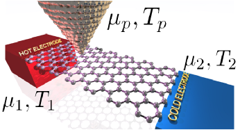
We consider junctions composed of a CNR or graphene molecule, hot and cold electrodes bonded to the molecule, a probe electrode, and the environment (see Fig. 1). The hot and cold electrodes provide a thermal gradient, but form an open electrical circuit in a thermal transport experiment. Under these conditions, and in linear response, the heat current flowing into the scanning thermal probe is Bergfield et al. (2013)
| (2) |
where is the temperature of terminal , is the thermal conductance between electrodes and , is the thermal coupling of the probe to the ambient environment at temperature , and is the phonon heat conductance between the probe and a phonon bath with temperature . The environment could be, for example, the black-body radiation or gaseous atmosphere surrounding the circuit, or the cantilever/driver on which the temperature probe is mounted Bergfield et al. (2013).
Eqs. (1) and (2) can be solved for the temperature of a probe in thermal and electrical equilibrium with, and coupled locally to the system of interest Bergfield et al. (2013)
| (3) |
Here the thermal conductance between electrodes and within the three-terminal thermoelectric circuit formed by the probe and hot and cold electrodes is Bergfield et al. (2013)
| (4) |
where is an Onsager linear-response coefficient, and .
We envision experiments performed in ultrahigh vacuum (UHV) with the electronic temperature probe operating in the tunneling regime and scanned across the sample at fixed height. Under linear-response conditions, electron-phonon interactions and inelastic scattering are weak in graphene, so the indirect phonon contributions to and can be neglected. Thermal transport from phonons is included via . The linear response coefficients needed to evaluate Eq. (3) may thus be calculated using elastic electron transport theory Sivan and Imry (1986); Bergfield and Stafford (2009)
| (5) |
where is the equilibrium Fermi-Dirac distribution with chemical potential and temperature . The transmission function Di Ventra (2008); Bergfield and Stafford (2009) is expressed in terms of the tunneling-width matrices and the retarded Green’s function of the junction , where the overlap matrix reduces to the identity matrix in an orthonormal basis and . Throughout this work we consider transport in the wide-band limit where .

In the vicinity of the Dirac point, a simple tight-binding Hamiltonian has been shown to accurately describe the -band dispersion of graphene Reich et al. (2002). The molecular Hamiltonian is
| (6) |
where is the nearest-neighbor hopping matrix element between 2pz carbon orbitals of the graphene lattice, and creates an electron on the ith 2pz orbital. To be specific, we consider here a scanning thermal microscope (SThM) with an atomically-sharp Pt tip operating in the tunneling regime but near contact. The tunneling-width matrix may be described in general as Bergfield et al. (2012) , where and label -orbitals of the molecule, is the local density of states on the apex atom of the probe electrode, and is the tunneling matrix element between the quasi-atomic apex wavefunction and orbital of the molecule. We consider all orbitals of the Pt SThM’s apex atom and the -system of the carbon sheet, meaning that the transport into the probe is multi-channel Bergfield et al. (2012).
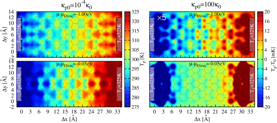
Results – The calculated local temperature distribution of an armchair CNR bonded to hot and cold electrodes held at =325K and =275K, respectively, is shown for several gate potentials and environmental coupling strengths in Fig. 2. In these calculations, the SThM is scanned 2.5Å above the plane of the carbon nuclei and the matrices describing the lead-molecule coupling are diagonal. Non-zero elements of , drawn as small red or blue circles in the figure, indicate contact between the electrode and the carbon atoms of the nanoribbon and are equal to 150meV. The probe is operating in the tunneling regime since the sum of Pt and C covalent radii is 2.03Å Lide et al. (2005). As indicated in the figure, the wavelength of the temperature variations changes as the quasiparticle energy is adjusted close to the Dirac point .
In the simulations presented here, we consider both a weak environmental coupling =, and a realistic environmental coupling =100, where ==0.284nW/K is the thermal conductance quantum at 300K Rego and Kirczenow (1998). The weak coupling value = corresponds to the radiative coupling between a tip with effective radius 100nm and the blackbody environment, a fundamental limit on Bergfield et al. (2013). At larger values of , the amplitude of the quantum temperature oscillations is reduced due to the reduced sensitivity of the thermal measurement Bergfield et al. (2013); Kim et al. (2012), but the qualitative features of the interference pattern are preserved. For comparison, the UHV SThM of Kim et al. Kim et al. (2012) recently achieved 700. The phonon heat conductance is small since the Debye frequency of Pt and the CNR’s phonon distribution are incommensurate and, at 2.5Å above the CNR, the probe is not in contact with the CNR. We consider a realistic value of =0.01, and let vary linearly between the hot and cold electrodes.

The spatial temperature variations are a consequence of quantum interference Dubi and Di Ventra (2009a), where the flow of heat from the hot and cold electrodes into the probe is determined by position-dependent interferences and the molecular density of states Bergfield et al. (2013). According to Eq. (3), a maximally hot spot will be observed whenever , and vice versa for a maximally cold spot. In general, the largest variations in temperature will be observed when the thermal conductance from one of the two electrodes into the probe is suppressed by destructive quantum interference Bergfield et al. (2013), which occurs when the phase between thermal transport paths differs by , so that . Such oscillations are ubiquitous in electron systems at low temperatures, the best known example being the Friedel oscillations in the density of states or charge density Xue et al. (2012).

Due to its unique dispersion relation, the Friedel oscillation wavelength in graphene depends strongly on the energy of the quasiparticles, which may be controlled via the application of a gate voltage Xue et al. (2012)
| (7) |
where is the energy away from the Dirac point. In our tight-binding Hamiltonian , where =2.7eV is the tight-binding matrix element and =1.42Å is the C-C distance Castro Neto et al. (2009). The power spectral density (PSD) of a slice through the center row of the CNR shown in the left panels of Fig. 2 is shown for =-1.00eV, -0.50eV, and -0.25eV in Fig. 3. As shown in the figure, a spectral peak shifts as changes, in good agreement with Eq. 7 (shown as vertical blue lines in the figure). Closer to the Dirac point, where the Friedel oscillation wavelength becomes comparable to the linear dimensions of the system simulated, it is not straightforward to resolve this peak above the background of peaks at small wavevectors arising from finite-size effects. Nonetheless, it is clear from Fig. 2 (lower panels) that the dominant wavelength of the temperature oscillations grows dramatically as .
The wide tunability of the temperature oscillations over orders of magnitude in wavelength in graphene indicates that they are within the spatial resolution of current SThM technology, which has achieved spatial and thermal resolution of 10nm and 15mK, respectively Kim et al. (2012), provided the phase coherence length of the carriers is sufficiently long. In pure graphene the dominant dephasing mechanism is deformation potential scattering by acoustic phonons Hwang and Das Sarma (2008). Using the scattering rate derived in Ref. Hwang and Das Sarma, 2008 and assuming that the momentum relaxation time is equivalent to the phase-relaxation time, the phase-coherence length is given by
| (8) |
where is the deformation potential, =2cm/s is the acoustic phonon velocity, 7.6g/cm2 is the graphene mass density, and 1.53m/s is the Fermi velocity. The deformation potential reported in the literature typically ranges from 10-30eV. As an example, with =30eV and =300K, (1.0eV)=68.4nm and (0.05eV)=1.36. These estimates, which are in good agreement with recent experimental phase-coherence length measurements of carbon nanoribbons Minke et al. (2012), clearly indicate that quantum thermal oscillations in graphene can occur on length scales well within the resolution of existing SThM techniques. Indeed, the more formidable experimental challenge is likely to be reducing the environmental coupling of the probe to increase the amplitude of the thermal oscillations above the threshold for observation (cf. Fig. 2).
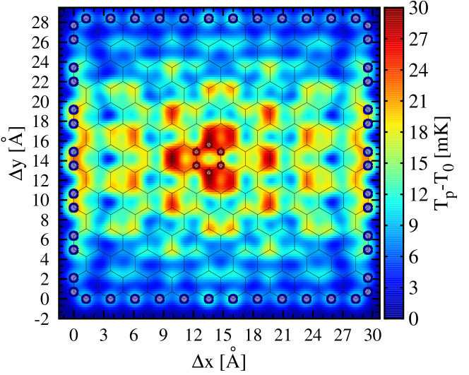
As a final example of an experimentally realistic system which may be used to investigate quantum temperature oscillations, we consider a graphene flake with a hot needle-like terminal in the center, and the edge of the flake held at ambient temperature. The temperature profile for this junction is shown in Fig. 4 for , corresponding to the current experimental sensitivity Kim et al. (2012). In Fig. 4, we have taken ; the predicted temperature profile exhibits a strong dependence on gate voltage and exhibits quantum oscillations within the resolution of current state-of-the-art SThM techniques. We stress that although computational resources have limited our discussion to small molecule structures, longer wavelength oscillations should be observable in larger systems provided the transport is phase coherent and coupling to the environment is minimized.
Conclusion – We have found that temperature oscillations in carbon nanoribbon and graphene junctions, like Friedel oscillations, can be tuned over orders of magnitude in wavelength, making this an ideal system for both fundamental and device related studies into the nature of temperature and heat transport at the nanoscale.
Work by J.P.B. and M.A.R. was supported as part of the Non-Equilibrium Energy Research Center (NERC), an Energy Frontier Research Center funded by the U.S. Department of Energy, Office of Science, Basic Energy Sciences under Award DE-SC0000989. C.A.S. acknowledges support from the U.S. Department of Energy (DOE), Basic Energy Sciences under Award No. DE-SC0006699. M.D. acknowledges support from the DOE under Grant No. DE-FG02-05ER46204.
References
- Altet et al. (2006) J. Altet, W. Claeys, S. Dilhaire, and A. Rubio, Proc. IEEE 94 (2006).
- Bischof (2006) J. Bischof, Heat Mass Transf. 42, 955 (2006).
- Chen et al. (2003) Y. Chen, M. Zwolak, and M. Di Ventra, Nano Lett. 3, 1691 (2003).
- Ming et al. (2010) Y. Ming, Z. X. Wang, Z. J. Ding, and H. M. Li, New J. Phys. 12, 103041 (2010).
- Galperin et al. (2007) M. Galperin, A. Nitzan, and M. A. Ratner, Phys. Rev. B 75, 155312 (2007).
- de Wilde et al. (2006) Y. de Wilde, F. Formanek, R. Carminati, B. Gralak, P.-A. Lemoine, K. Joulain, J.-P. Mulet, Y. Chen, and J.-J. Greffet, Nature 444, 740 (2006).
- Yue et al. (2011) Y. Yue, J. Zhang, and X. Wang, Small 7, 3324 (2011).
- Greffet and Henkel (2007) J.-J. Greffet and C. Henkel, Contemp. Phys. 48, 183 (2007).
- Engquist and Anderson (1981) H.-L. Engquist and P. W. Anderson, Phys. Rev. B 24, 1151 (1981).
- Dubi and Di Ventra (2009a) Y. Dubi and M. Di Ventra, Nano Lett. 9, 97 (2009a).
- Bergfield et al. (2013) J. P. Bergfield, S. M. Story, R. C. Stafford, and C. A. Stafford, ACS Nano 7, 4429 (2013).
- Büttiker (1989) M. Büttiker, Phys. Rev. B 40, 3409 (1989).
- Cahill et al. (2003) D. G. Cahill, W. K. Ford, K. E. Goodson, G. D. Mahan, A. Majumdar, H. J. Maris, R. Merlin, and S. R. Phillpot, J. Appl. Phys. 93, 793 (2003).
- Cahill et al. (2002) D. G. Cahill, K. Goodson, and A. Majumdar, J. Heat Transfer 124, 223 (2002).
- Dubi and Di Ventra (2009b) Y. Dubi and M. Di Ventra, Phys. Rev. B 79, 115415 (2009b).
- Dubi and Di Ventra (2009c) Y. Dubi and M. Di Ventra, Phys. Rev. E 79, 042101 (2009c).
- Kim et al. (2011) K. Kim, J. Chung, G. Hwang, O. Kwon, and J. S. Lee, ACS Nano 5, 8700 (2011).
- Yu et al. (2011) Y.-J. Yu, M. Y. Han, S. Berciaud, A. B. Georgescu, T. F. Heinz, L. E. Brus, K. S. Kim, and P. Kim, Appl. Phys. Lett. 99, 183105 (2011).
- Kim et al. (2012) K. Kim, W. Jeong, W. Lee, and P. Reddy, ACS Nano 6, 4248 (2012).
- Menges et al. (2012) F. Menges, H. Riel, A. Stemmer, and B. Gotsmann, Nano Lett. 12, 596 (2012).
- Xue et al. (2012) J. Xue, J. Sanchez-Yamagishi, K. Watanabe, T. Taniguchi, P. Jarillo-Herrero, and B. J. LeRoy, Phys. Rev. Lett. 108, 016801 (2012).
- Dubi and Di Ventra (2011) Y. Dubi and M. Di Ventra, Rev. Mod. Phys. 83, 131 (2011).
- Sánchez and Serra (2011) D. Sánchez and L. Serra, Phys. Rev. B 84, 201307 (2011).
- Jacquet and Pillet (2012) P. A. Jacquet and C.-A. Pillet, Phys. Rev. B 85, 125120 (2012).
- Caso et al. (2011) A. Caso, L. Arrachea, and G. S. Lozano, Phys. Rev. B 83, 165419 (2011).
- Sivan and Imry (1986) U. Sivan and Y. Imry, Phys. Rev. B 33, 551 (1986).
- Bergfield and Stafford (2009) J. P. Bergfield and C. A. Stafford, Phys. Rev. B 79, 245125 (2009).
- Di Ventra (2008) M. Di Ventra, Electrical transport in nanoscale systems (Cambridge University Press, 2008).
- Reich et al. (2002) S. Reich, J. Maultzsch, C. Thomsen, and P. Ordejón, Phys. Rev. B 66, 035412 (2002).
- Bergfield et al. (2012) J. P. Bergfield, J. D. Barr, and C. A. Stafford, Beilstein J. Nanotechnol. 3, 40 (2012).
- Lide et al. (2005) D. R. Lide et al., ed., CRC Handbook of Chemistry and Physics (CRC Press, Boca Raton, Fla., 2005).
- Rego and Kirczenow (1998) L. G. C. Rego and G. Kirczenow, Phys. Rev. Lett. 81, 232 (1998).
- Castro Neto et al. (2009) A. H. Castro Neto, F. Guinea, N. M. R. Peres, K. S. Novoselov, and A. K. Geim, Rev. Mod. Phys. 81, 109 (2009).
- Hwang and Das Sarma (2008) E. H. Hwang and S. Das Sarma, Phys. Rev. B 77, 115449 (2008).
- Minke et al. (2012) S. Minke, J. Bundesmann, D. Weiss, and J. Eroms, Phys. Rev. B 86, 155403 (2012).