Characterizing the rate and coherence of single-electron tunneling between two dangling bonds on the surface of silicon
Abstract
We devise a scheme to characterize tunneling of an excess electron shared by a pair of tunnel-coupled dangling-bonds on a silicon surface – effectively a two-level system. Theoretical estimates show that the tunneling should be highly coherent but too fast to be measured by any conventional techniques. Our approach is instead to measure the time-averaged charge distribution of our dangling-bond pair by a capacitively coupled atomic-force-microscope tip in the presence of both a surface-parallel electrostatic potential bias between the two dangling bonds and a tunable mid-infrared laser capable of inducing Rabi oscillations in the system. With a nonresonant laser, the time-averaged charge distribution in the dangling-bond pair is asymmetric as imposed by the bias. However, as the laser becomes resonant with the coherent electron tunneling in the biased pair the theory predicts that the time-averaged charge distribution becomes symmetric. This resonant symmetry effect should not only reveal the tunneling rate, but also the nature and rate of decoherence of single electron dynamics in our system.
pacs:
68.37.Ps, 66.35.+a, 71.55.-i, 03.67.-aI Introduction
Two closely spaced quantum dots can function as an effective two-level system when they share an extra electron via coherent tunneling. Such a system is also known as a “charge qubit” and its various physical implementations have been explored with applications to quantum computing,Nakamura et al. (1999); Hollenberg et al. (2004); Hayashi et al. (2003) spin-charge conversion Hayashi et al. (2003); Gorman et al. (2005) for spin-qubit readout,Elzerman et al. (2004) and in general for engineering new devices on silicon surfaces at the quantum level.Schofield et al. (2013) Although solid-state charge qubits have been demonstrated in semiconductors and superconductors,Nakamura et al. (1999); Wallraff et al. (2005) in practice their properties exhibit uncontrolled and undesired variability (of the single dot and of the entire assembly) due to growth imperfections and decoherence mechanisms.
We have suggested overcoming these challenges by employing silicon-surface dangling bonds (DBs) as tunnel-coupled quantum dots sharing a controllable number of electrons Haider et al. (2009). All such dots are identical and their spacing is determined with atomic-scale precision. An excess electron shared in a pair of such DBs is predicted to be highly coherent with a tunneling period between 10 fs and 1 ps.Livadaru et al. (2010); Pitters et al. (2011a) Furthermore, the fabrication of relatively large assemblies of DBs can be achieved by using a scanning tunneling microscope with great precision, reliability, reproducibility, and virtually no variability at the single dot level.
However, the very same feature that leads to high coherence, namely the great rate of tunneling, also gives rise to some considerable practical difficulties in that direct characterization by monitoring the oscillation is not feasible electronically by any straightforward methods. Here we propose a strategy to measure the rate and coherence of tunneling by controlling and monitoring time-averaged charge distributions in pairs of coupled DB dots.Gardner et al. (2011) These measurements are inspired by previous experiments on double quantum-dot structures with tunneling rates in the microwave regime.Petta et al. (2004); Stace et al. (2005)
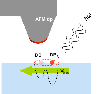
A DB pair can be created such that electrostatic repulsion prevents an excess electron acquired at each DB (i.e. net charge per pair), and DBs are sufficiently close so that they are tunnel-coupled with each other. The DB pair can thus be geometrically tuned to have the desired occupation of one extra electron per pair, and henceforth we call it DBP- for convenience. In our approach, the electron’s position within the ‘left’ (L) or ‘right’ (R) dot is discerned by an atomic force microscope (AFM) capacitively coupled to the pair.
Atomic force microscopy can achieve single-electron sensitivityGardner et al. (2011); Zhu et al. (2005) and recently it has been used for detecting the electronic properties of individual and coupled quantum dots in contact with a reservoir.Cockins et al. (2010, 2012) A tunnel-coupled DB system is analogous to these coupled quantum dot system, but on a smaller spatial scale. As such, they exhibit molecular state formations as in quantum dot systems or in “natural” molecules. Similar to other quantum dot systems, artificially fabricated DB bonds offer the possibility of choosing bond strength (tunnel splitting) via their geometry. Unlike conventional chemical bonds, the through-space bonding occurs partly in vacuum and partly in the silicon dielectric medium. Such a particular flavor of bond will no doubt be the subject of investigations beyond the scope of this study.
An alternative but equivalent picture is that of coupled DB pairs with electrons tunneling coherently between individual DBs. As the AFM measurements are in practice relatively slow on the time scale of the DB pair charge dynamics, they average over many oscillations thereby losing all direct information about the tunneling rate and decoherence. Effectively, during such a measurement, capacitive coupling to the DBP- induces an anharmonic component in the potential on the AFM tip, which is otherwise harmonic in the absence of capacitive coupling to localized charges.Giessibl (2003) Importantly, the strength of this coupling reveals the time-averaged charge in the left (and right) dot and is manifested as a shift in the AFM oscillation frequency.
By using lithographic contacts on a silicon surface, it is generally possible to apply electric potential biases in order to locally address single atoms and molecules.Fuechsle et al. (2012); Zikovsky et al. (2011); Pitters et al. (2011b) Such contacts can be used to establish an electric field along the two DBs in a DBP-. This bias will cause the probability distribution for the position of an excess electron to be more heavily weighted in the left or right DB depending on the sign and strength of the bias. In our scheme it is exactly this distribution that is observable by AFM. Furthermore, the actual tunneling rate is influenced by this static bias. For zero bias the position of the excess electron is equally probable in the right and left DB.
In order to experimentally determine tunneling rate and decoherence, another ingredient is needed: an oscillatory driving force pushing the excess electron back and forth rapidly between the two DBs at a rate comparable to the native tunneling frequency of the DBP-. In the case of two DBs, the driving field needs to be in the mid-infrared (MIR) regime.
If the MIR field is off-resonant with the inter-dot tunneling frequency, the resultant force has only a small perturbative effect on the double-dot system so that the excess electron distribution is nearly the same as that without a driving field. If the MIR radiation is resonant, it can be theoretically shown that its field causes the electron to be equally probable at either DB. As one varies the frequency of the driving field, the above effect results in a relatively abrupt change in the excess electron distribution and causes an equally abrupt change in the AFM tip-oscillation frequency, which can be measured experimentally. The response of the AFM tip should reveal the tunneling rate and some properties and parameters of decoherence. The remainder of this paper elaborates on this concept and provides the technical details of our approach.
II Background
The scheme comprises a DBP- subject to a static potential bias, an AFM tip capacitively coupled to the DBs, and a MIR driving field. In this section we discuss technical issues concerning each component of the proposed apparatus.
II.1 Dangling bond on H–Si(100)–21
Each Si atom on a H–28Si(100)–21 surface shares two bonds with bulk Si, has one dimer bond with another surface Si and a fourth bond with a surface H, which can be removed thereby creating a DB.Tong and Wolkow (2006); Thoms and Butler (1995); Buehler and Boland (2000) Dangling bonds are readily created on the surface of silicon by using a scanning tunneling microscope (STM) to remove hydrogen atoms. We focus on the well studied case of DBs on the H–28Si(100)–21 surface Haider et al. (2009) depicted in Fig. 2.
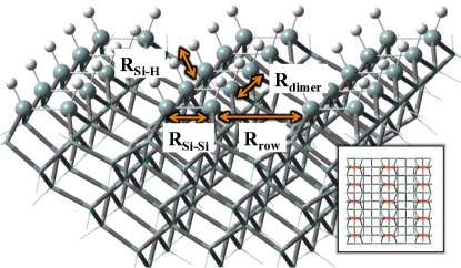
Ab initio calculations and experimental observations reveal that the Si-Si dimer bond is Å, the Si-H bond is Å, the distance between adjacent dimers is Å, and the distance between adjacent rows is Å, which is Å with Å the unit cell length in Si.Pitters et al. (2011a)
The DB can be created on a H–28Si(100)–21 surface by selectively removing a surface H atom by applying a voltage pulse using an STM tip.Haider et al. (2009); Pitters et al. (2011a); Livadaru et al. (2010) Structural and electronic properties of DBs have been studied extensively.Tong and Wolkow (2006); McEllistrem et al. (1998); Buehler and Boland (2000)
Ab initio calculations show that a neutral DB located on a H–28Si(100)–21 surface has only one confined electron with an energy located within the Si bandgap.Livadaru et al. (2010) This eigenstate is decoupled from the Si conduction and valence bands, resulting in a sharply localized electron wavefunction, which makes the DB amenable to electronics applications such as a quantum dot.
A DB can lose its single electron to the bulk, thereby becoming a positively charged DB+, or it can host one excess electron (with opposite spin) from the bulk, hence becoming negatively charged DB-. Losing or acquiring charge depends on the type and amount of doping in the host crystal, and on temperature. In our case, the crystal has a high concentration of n-type phosphorous (P) doping, cm-3; therefore, each DB is highly likely to carry an excess electron. Due to the on-site Coulombic energy, the level is shifted upward in energy by eV relative to the neutral DB level, but remains within the bandgap.Haider et al. (2009)
II.2 Dangling bond pair with a shared excess electron
As mentioned above, although an individual isolated DB is highly likely to be negatively charged, for DB pairs with a separation less than 16 Å, strong Coulombic repulsion between the excess electrons on the two DBs destabilizes such a charge configuration (with per DB pair). The DB pair re-stabilizes by losing one of the excess electrons into the Si conduction band. The resulting configuration is the DBP- with the excess electron shared between the two DBs by tunnel coupling.
Ab initio calculations show that the two lowest lying energy levels of the DBP- are situated within the silicon bandgap. Livadaru et al. (2010) The excess electron tunnels between the two DBs with a tunneling frequency , which is a function of the DB separation distance as well as of the potential barrier height between them. For small DB separations, this barrier is narrow and low, only a few tenths of an eV.
In addition to the upper bound for the DBP- separation, the geometry of the surface reconstruction also sets a lower bound,Tong and Wolkow (2006); Haider et al. (2009); Hitosugi et al. (1999) see Fig. 2. This minimum separation is Å, i.e. the dimer-dimer separation along the dimer row. These minimum and maximum separations result in an upper and lower bound, respectively, on the tunneling frequency of the excess electron given byLivadaru et al. (2010)
| (1) |
II.3 Coupled dangling bond pair as a quantum-dot charge qubit
A single bound electron shared between left and right DBs can behave as a two-level system, in the sense that, in the position representation, the states of the system can be given in terms of the orthogonal left and right states, or superpositions thereof. This two-level DBP- system can be also thought of as a double-well potential where the individual wells corresponds to left and right DB with quantum states and , respectively.Hayashi et al. (2003); Gorman et al. (2005) This two-level approximation holds if energy levels of each potential well are widely spaced so that only the ground states of each well are involved in the quantum superposition.
A useful alternative to the left-and-right basis is the basis corresponding to symmetric and antisymmetric states, and antisymmetric , respectively, which are eigenstates of the Hamiltonian in the absence of biasing fields. The left and right states can be recovered according to
| (2) |
Based on ab initio calculations, the energies of the symmetric and antisymmetric states are within the silicon band gap.Livadaru et al. (2010) The higher energy levels are all above the silicon band gap so that an electron will become delocalized in the silicon conduction band, rather than assuming a localized excited state; hence the two-level system approximation, including loss, yields an excellent model.
We are now ready to construct the Hamiltonian for coherent dynamics of the charge qubit. For and the on-site energies plus local field corrections for the left and right DBs respectively, the free Hamiltonian for uncoupled DBs is . We assume that (a symmetry condition) The Hamiltonian for coherently coupled DBs is
| (3) |
Diagonalizing yields eigenenergies with corresponding eigenstates , respectively.
III Dangling bond pair under static bias and driving laser field
III.1 Static bias
Applying a static bias to DBP- enables one to control the tunneling rate in the system by creating an energy offset between the left and right DB while preserving the local confinement potential characteristics at each well as depicted in Fig. 1. This bias is physically implemented by local electrodes in the vicinity of the DBP-.
The Hamiltonian of a DBP- subjected to a static bias is given byvan der Wiel et al. (2002)
| (4) |
with
| (5) |
and where is the identity matrix. Diagonalizing the biased Hamiltonian for the DBP- (III.1) yields
| (6) |
and
where
The resultant modified tunnelling frequency is thus
| (7) |
and the time-averaged charge distribution on the left dot is
| (8) |
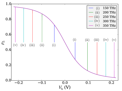
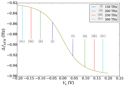
which is depicted as the solid black line in Fig. 3. As expected, the charge distribution is equal for the two DBs when the electric potential bias is zero.
III.2 Mid-infrared driving field
We now add a MIR driving field with frequency to the scheme as shown in Fig. 1. The purpose of this driving field is to probe the system to discover resonance conditions whereby the barrier between the left and right DBs effectively vanishes.Petta et al. (2004) A tunable continuous-wave solid-state laser or CO2 gas laser are examples of suitable MIR sources.Curl and Tittel (2002) The MIR beam intensity must be weak enough to ensure that multi-photon resonances are negligible,Petta et al. (2004); Stace et al. (2005) but strong enough to drive the oscillation between left and right DBs.
A quantitative description of the dynamics begins by treating the biased DBP- as an electric dipole with an approximate transition dipole moment , which is the product of the electron charge and the inter-DB separation vector pointing from the negative to the neutral DB. The corresponding dipole-moment operator is .
The electric-dipole interaction with the MIR electric field is given by the interaction Hamiltonian Allen and Eberly (1975)
| (9) |
The interaction strength is quantified by the Rabi frequency
| (10) |
and the resultant driving-field interaction Hamiltonian is Barrett and Stace (2006)
| (11) |
for a parameter containing information about the laser beam angle and ratio of wavelength to dipole length.
The intensity of the radiation is related to the Rabi frequency via the electric-field amplitude, with the permittivity, the electric-field amplitude, and the speed of light. Assuming that and are parallel, Eq. (10) yields
| (12) |
For a DBP- with inter-DB distance Å, we obtain Cm.
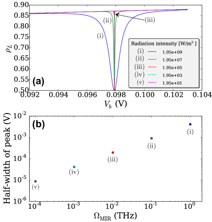
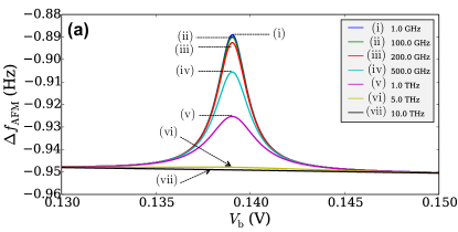
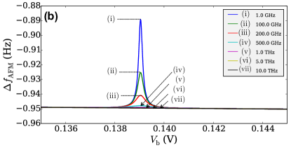
In addition to the conditions above, the Rabi frequency is low enough to avoid multi-photon resonances but high enough to drive the oscillation, and the choice offers some flexibility to tune these parameters. We therefore studied the effects of the intensity of the applied laser in Fig 4, where we varied this quantity over a few orders of magnitude.
We can see in this figure that, as the intensity is decreased, the width of the resonance peaks decreases as well. Eventually the width becomes lower than the noise in the applied bias, for a laser intensity of about 20 W/m2. The horizontal resolution of the resonance was estimated by treating the width as being due to thermal noise in the biasing electrodes, namely the Johnson-Nyquist noise given by the formula
| (13) |
for M, and kHz, similar to values present in an STM instrumental setup. The corresponding Rabi frequencies for each peak width are plotted in Fig 4(b) (anticipating that this is also the range of useful Rabi frequencies for the purpose of this study, i.e. 0.1 GHz to 1 THz.)
Corresponding radiation intensities ranging from 20 to W/m2) are experimentally feasible with current CO lasers. CO lasers are high-power, continuous-wave lasers that generate infrared light with wavelength within the domain of 9.2–11.4 m, corresponding to a frequency range of 165–205 THz, and have an operating power from mW to hundreds of W.
III.3 The combined action of static bias and driving field
The Hamiltonian including both the static bias and the driving field is
| (14) |
Converting to the interaction picture according to
eliminates explicit time dependence. If the detuning is small compared to the frequency sum , then Barrett and Stace (2006)
| (15) |
where
| (16) |
for a weak MIR field, namely .Allen and Eberly (1975)
The eigenenergies of the approximate interaction Hamiltonian in (15) are Barrett and Stace (2006)
| (17) |
which represent the modified Rabi frequencies. The corresponding eigenstates are
| (18) |
for
| (19) |
The probability for the charge to be on the left DB is
| (20) |
analogous to the undriven distribution (8).
In an actual experiment, for a given MIR frequency , the potential bias is adjusted until a resonance is found whereby the charge distribution is equal on the two DBs. Thus, one is expected to obtain curves similar to those in Fig. 3, where the spikes correspond to cases that . Intuitively, these resonances correspond to the MIR driving field overwhelming the biasing field, effectively making the barrier negligible and the charge distribution equal in either DB.
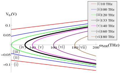
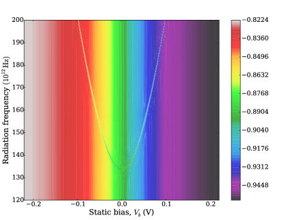
Figure 5 shows an extended parameter space as contour plots of loci where, for fixed values of indicated in the legend, resonances such as those in Fig. 3 occur. This figure illustrates a key point of our scheme, namely that the MIR frequency and potential bias can be tuned to discover the tunneling frequency simply by measuring the probability of the excess charge being in the left DB.
IV Mitigating laser heating
Excessive heating by the incident laser radiation can lead to damage of the sample. An important detail when estimating laser damage in our sample is that we only require radiation with sub-bandgap energy, for which the silicon absorption coefficient is relatively small. Therefore, silicon crystals are resilient to heating and have a high thermal and optical damage thresholdRaghunathan et al. (2006) in the MIR range of interest due to low absorption for this spectral domain.
For the H–Si(100) substrate in our study, above-bandgap driving radiation (= 532 nm) with an intensity of 2.67 W/m2 suffices to cause hydrogen desorption but does not damage the sample.Schwalb et al. (2007) Given that we require sub-bandgap radiation (= 9-19 m) with two orders of magnitude lower intensity, any damage to the sample is expected to be highly unlikely. At these greatly reduced intensity levels, hydrogen desorption is also unlikely. Schwalb et al. (2007)
However, for a real sample the specific type and number of defects might be generally unknown, and other heating mechanisms might be at play. For the case when a high Rabi frequency (1 THz and higher) is required in order to induce measurable resonance peaks, the correspondingly high laser intensity might be of practical concern inasmuch as a prolonged laser exposure is required during the experiment. Therefore, we here estimate theoretically the effects of laser heating under those conditions, and suggest ways to deal with them.
The flow of heat can be modeled by the heat equation Carslaw and Jaeger (1959)
| (21) |
where , is the temperature function, is the mass density, is the specific heat, is the thermal conductivity, and is the heat-source term related to the power density injected by the laser into the sample. Note that the material constants appearing in these coefficients are generally functions of temperature, but here they were assumed to be constant.
The source term varies spatially with the depth into the sample, according to the power absorbed from the incident laser as
| (22) |
where is the decay rate of the radiation intensity in the sample, is the transmission coefficient at the surface, is the intensity of the incident radiation, and is the location of the surface.
We solve the boundary value problem (BVP) consisting of the above heat equation and appropriate boundary conditions (BCs) by the finite element method on a two-dimensional -grid spanning a region. We solve this BVP for consecutive time slices using an Euler scheme for sampling time evolution. We use the esys-escript FEM library Gross et al. (2007) for getting the numerical solution.
Given that the choice of BCs has a drastic effect on the evolution of the temperature in our system, we explored various setups for the purpose of minimizing the heating effect. We find the most favorable BC to be a Dirichlet-type condition at the back of the sample, where we set the temperature to a fixed value of 4 K, i.e. simulating the effect of a liquid-helium-cooled metal plate in thermal contact with the back of the Si sample. For this setup, we obtain the time evolution shown in Fig. 6 for the temperature profile as a function of the depth into the sample.
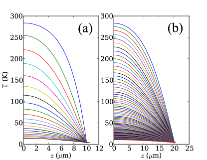
A laser of total power 1 W is focused on an area of m2, corresponding to an intensity of W/m2, chosen higher than any intensity expected in the actual experimental situation. Material parameters used in the simulation are the following: thermal conductivity of Si: 149 W/K-m; mass density of Si: 2329 kg/; specific heat of Si: 814 J/kg-K; complex refractive index of Si: with = 3.4215, for a frequency of 100 THz.Palik (1985) Note that the above value of the refractive index corresponds to low- to medium-doped Si. In general, the value of the absorption coefficient in the infrared range depends strongly on the doping level and can become greater than 2000 cm-1 for donor concentrations above 1019 cm-3.Spitzer and Fan (1957) However, in our proposed setup, doping is only practically required in a very thin topmost layer, resulting in negligible heating, as calculated.
In order to eliminate any doubts about the role of the exact thermal resistivity gradient at the cooler boundary, we simulated the same system with this boundary placed at different depths from the silicon surface, 10 and 20 m, with results shown in Fig. 6 (a) and (b), respectively. As expected, the thicker sample in (b) takes a few times longer to cool, but it ends up saturating to a cool profile nonetheless. The same cooling behavior is present for a cool reservoir at 4 K or 77 K.
To sum up, our simulations show that even in the presence of laser radiation, our sample cools off to a steady profile in a few microseconds if the cool boundary is placed a few tens of m from the silicon surface. Therefore we expect excessive heating can be avoided by using a cooling system even in cases with the most intense radiation required for our experimental apparatus.
V Atomic force microscopy characterization of tunneling between dangling bonds
AFM is ideally suited to measure the spatial charge distribution in a DBP- (Fig. 1) without significantly distorting the electronic landscape of the sample. The AFM has been shown to detect single charges.Cockins et al. (2009); Stomp et al. (2005)
V.1 Modeling atomic force microscope in frequency modulation mode
The AFM cantilever behaves as a simple harmonic oscillator along the coordinate axis perpendicular to the sample surface. The tip is driven by an externally controlled force , with being constant. When scanning a sample, the AFM tip experiences distance-dependent forces from its interaction with the sample.
In the limit of small oscillation amplitudes and small force gradients, the equation of motion for the AFM tip around its equilibrium position (chosen as the origin of the -axis, at a height from the surface) is Marchi et al. (2008)
| (23) |
where is the AFM damping factor, the mass of the probe and
| (24) |
the AFM probe spring constant.
In the same limit of small oscillation amplitudes (a few Å is anticipated), we can use a truncated Taylor expansion
| (25) |
with a resultant equation of motion for the tip,
| (26) |
describing driven oscillations with a modified resonant frequency depending on the lateral tip position
| (27) |
The right-hand side of Eq. (26) is a constant in space so the tip-sample force is detected by measuring the frequency response of the tip according to (27). Employing the binomial expansion on Eq. (27) yields the modified frequency expression
| (28) |
showing the proportionality between the frequency shift and the local force gradient.
Note that far from the limit of small amplitudes one can still approximate the AFM motion from the above equation, but instead of the force gradient at the equilibrium position, one should use an average force gradient over an entire oscillation range , i.e.
| (29) |
The experimental goal is then to measure these changes in the tip oscillation frequency thereby revealing information about the sample.
From Eq. (28), we see that the ratio gives the sensitivity of the cantilever, which in practice depends on the build geometry and material of the cantilever. Typical examples are silicon cantilevers with a sensitivity factor Hz m/N, and the qPlus tuning fork with Hz m/N.Morita et al. (2009); Giessibl (2003); Gross et al. (2009) However, when choosing a cantilever for a given experiment, the sensitivity is not the only factor to consider, as scan stability (e.g. against jump-to-contact), quality factor, measurement bandwidth, and appropriate size of oscillation amplitudes also play important roles.
The minimum detectable signal of an AFM experimental setup is determined by assessing its frequency noise , i.e. the standard deviation of the frequency shift. Theoretically, is given bySchneiderbauer et al. (2012); Kobayashi et al. (2011)
| (30) |
where is the quality factor, is the oscillation amplitude, is the measurement bandwidth, is the thermal energy, and is the deflection noise density. The first term on the right-hand side of Eq. (30) is the thermal noise of the AFM tip, the second term is the deflection-detector noise, and the third term is the noise of the instrumental setup. Thus, one should choose the experimental parameters such that the sensitivity and the signal-to-noise ratio of the AFM setup are optimized.
V.2 Tip-sample interactions
In using the AFM to measure the charge distribution at the silicon surface, all significant tip-sample forces must be considered by our model. These can be short-range chemical forces (less than 5 Å), long-range van der Waals forces, electrostatic forces, or magnetic forces (up to 100 nm).Giessibl (2003) However, we choose operational parameters to ensure that electrostatic forces produced by the DBP- dominate over these other forces.
The external source potential is kept constant during the interaction with the sample. If the tip is sufficiently far from the surface, chemical forces can be ignored, and magnetic forces are negligible if the tip is made of non-magnetic material, e.g. tungsten. An ultrasharp nanotip Rezeq et al. (2006) is employed to minimize forces arising from induced polarization of the sample. Reducing the tip oscillation amplitude to the Ångstrom scale, for example with a quartz-made qPlus sensor,Morita et al. (2009); Giessibl (2003); Gross et al. (2009) also helps to minimize this form of interaction.
V.3 Trapped charge in the tip-sample system
V.3.1 Electrostatic potential energy
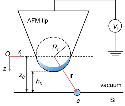
The DBP- can be treated as a trapped charge oscillating between the left and right DBs. This single charge is located within the plane of the Si surface (Fig. 7). Thus, the charge interacts with other entities such as the space-charge layer in the semiconductor substrate and other charges in the substrate and on the biased AFM tip, if present. Here we analyze the problem from a basic viewpoint in order to capture the essential electrostatic elements at play.
For an n-type Si sample with a donor concentration, the presence of a locally planar electrode at a height above the surface biased at a voltage induces a subsurface space-charge layer in the semiconductor with a width approximated by the solution of the quadratic equationFeenstra (2003)
| (31) |
where and are the vacuum permittivity and semiconductor dielectric constant, respectively.
Correspondingly, the so-called band bending potential at a depth into the sample can be written in the quadratic approximation as Feenstra (2003)
| (32) |
where is the potential at the surface given by
| (33) |
where ‘sign’ gives the sign of the applied tip bias. As the AFM tip is usually not locally planar the above equation is a coarse approximation for band bending representing an upper limit for the real case.
In order to calculate the potential at the Si surface, we approximate the electrostatic potential due to the biased AFM tip as being that of a biased conducting sphere with radius fitted to the apex region of the tip (or the “boss” as depicted in Fig. 7). In order to reflect the contribution of the mobile charge carriers in the substrate, we apply a rescaling of this spherical potential, namely we recalibrate the value of the potential at the Si surface location directly under the tip apex, , to be just given above.
From this analysis, at the location of the DB, the bare potential due to the tip is
| (34) |
where the coordinate origin is chosen at the center of the boss sphere. This bare potential does not include the image charge effects, which are accounted for below. Furthermore, for the case when the amplitudes of the AFM cantilever are small, we can neglect the variation of with the tip height and use henceforth only its value at the equilibrium scanning height.
With the above assumptions, the effective electrostatic energy of the tip-charge system can be written as Kantorovich et al. (2000)
| (35) |
where the last term accounts for the image charge inside the tip and for the charge redistribution via the voltage source as explained by Kantorovich et al.Kantorovich et al. (2000) (note the change in the unit system used here). Then the force exerted on the tip in the direction normal to the surface can be calculated as
| (36) |
This expression for force can then be substituted into Eq. (24) to approximate the expected AFM frequency shift.
V.3.2 Atomic-force-microscope frequency shift
The AFM frequency shift is obtained from the derivative of the force with respect to , as in Eq. (28)
| (37) | |||||
In readout of a DBP- excess charge, the total AFM frequency shift is given by
| (38) | ||||
where () is the frequency shift due to the charge localized in the left (right) DB and each frequency shift is weighted by the corresponding time-averaged charge probability . The parameter is the differential frequency shift of the cantilever caused by the excess charge tunneling from the right to the left DB; i.e.
| (39) |
Equation (38) indicates that the AFM readout is linear in . Thus, we expect to observe resonances in the AFM output signal while scanning through a range of bias values , owing to the existence of resonance features for as seen in Fig. 3.
Note that the task of sensing the location of a single charge as in previous experimental work Gross et al. (2009) is different from the current task, where we attempt to obtain information about both the location and the rates of (driven) motion of the electron. However, this does not violate the uncertainty principle as we are not measuring the location and momentum of the particle, but rather time-averaged quantities, and the ultimate knowledge we aim to obtain of the quantum system is statistical in nature.
In order to optimize the AFM read-out, we judiciously choose experimental parameters. First, the AFM cantilever parameters should be chosen so that the noise is much lower than the signal. Second, for a given cantilever, we choose an appropriate oscillation amplitude for the AFM tip. Larger amplitudes yield lower noise, whereas lower amplitudes offer better spatial resolution. Finally, should be maximized with respect to to achieve the largest possible frequency-shift read-out.
Although the greater sensitivity of silicon cantilevers is certainly a desirable feature for the purpose of the current study, at present it seems unlikely that they would allow the required atomic resolution mainly due to their inability to achieve low-amplitude oscillations and thus perform scans very close to the sample, 1-2 nm. Attempting such tasks would likely lead to undesired frequent jump-to-contact events and thus very poor scans.
On the other hand, the qPlus tuning-fork system, although less sensitive, has been already proven to sense single charge with atomic spatial resolution Gross et al. (2009) due to its robustness and ability to scan very close to the sample at low amplitudes. (It easily avoids certain problems such as the jump-to-contact issue.Giessibl (1997)) It also allows combined AFM/STM studies thus facilitating DB fabrication and precise positioning during the experiment. Therefore in this study we choose parameters representative of the qPlus system, keeping in mind that the optimal system may have characteristics somewhere in between those of the tuning fork and silicon cantilevers.
As experimental values, we henceforth assume kHz, N/m, , 5 nm, 0 V, and operation at liquid helium temperature. Also, unless otherwise specified, the oscillation amplitude and equilibrium height for the AFM tip are assumed to be 3 Å and 1 nm, respectively. The total noise in the frequency shift signal estimated for all the results below is less than 5 mHz at 4 K and 9 mHz at 77 K. As the AFM experiments yield the frequency shift in units of Hz, we present our results below in terms of .
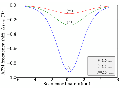
For a DBP- with separation of Å, the AFM maximum differential-frequency shift is obtained when the left dangling-bond is Å away from the AFM tip central axis. Figure 8 depicts the AFM frequency shift as a function of the lateral tip position . In this figure, it is clear that the effect of a trapped charge on the value of the AFM frequency is highly dependent on tip height. The great increase in signal for a tip height less than 1 nm is due to the fact that image-charge forces dominate in such close proximity to the localized charge.
Note that despite the simplicity of our model, the calculated magnitude of the signal is commensurate with past experimental results of single-charge sensing with atomic resolution.Gross et al. (2009) Hence, this scheme is appropriately sensitive to small displacements of single trapped charge.
Figure 9 shows the resonant peaks in the AFM signal. These resonant features are reflected in the oscillation frequency of the AFM tip when the DBP- is simultaneously exposed to a static bias and a driving radiation. In fact, the resonances can be exploited by varying the static bias for a fixed driving frequency. For each value of driving frequency a pair of resonant peaks appear on the AFM signal for two symmetric static-bias values. These peaks contain information about our system and can be used to determine the tunneling frequency of the excess charge.
More generally, Fig. 10 shows the AFM frequency shift as we sweep both the MIR driving frequencies and the applied static bias from a negative to a positive value. The resonance loci appear here as ridges (trenches) when the MIR driving frequency is commensurate with the ramped tunneling frequency. These resonance trends mirror the parabolic relationship between the MIR driving frequency and the static bias, as shown in Fig. 5.
VI Damped dangling bond pair dynamics
Until now our analysis ignores noise causing decoherence in the two-level system. In this section we study the effect of noise on the shape and width of the resonances used to characterize electron tunneling. We show that the noise model can be tested by the measurements, and we consider the specific model of spin-boson coupling Caldeira and Leggett (1981) to illustrate how the model is tested and the parameters are acquired by measurement.
The spin-boson model characterizes weak coupling between a two-level system and a generic bosonic bath, such as phonons or charge fluctuations.Caldeira and Leggett (1981) It is described by the Hamiltonian
| (40) |
with the oscillator frequency, and the corresponding creation and annihilation operators, and the coupling strength between the dangling-bond pair and the bath.
The first term on the right-hand side of Eq. (40) is the free bath Hamiltonian, and the second term is the system-bath interaction Hamiltonian. The interaction Hamiltonian indicates that the coupling depends linearly on the coordinates of the dangling-bond pair and the bath harmonic oscillators. The total Hamiltonian of the system would then be
| (41) |
where the first two terms are given in Eqs. (III.1) and (III.2).
Solving the Lindblad master equation for the dangling-bond pair,Lindblad (1976) the steady-state probability for the excess charge to be in the left quantum dot is Barrett and Stace (2006); Stace et al. (2005)
| (42) |
with decoherence rate for relaxation rate and dephasing rate . For and , Eq. (42) reduces to Eq. (20). In another limit, the relaxation rate and dephasing rate are equal up to second order in the limit of weak qubit-bath coupling: .
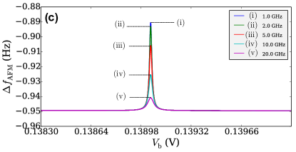
The AFM frequency shift is shown in Fig. 11 as a function of static bias for MIR driving frequency fixed to 250 THz and various decoherence rates given in the legends. As the Rabi frequency is sampled in decreasing order over three orders of magnitude in (a), (b), and (c), we notice strong narrowing of the resonance peaks,also seen in Fig. 4 in the absence of any decoherence.
A different range of the decoherence rate was sampled in each case in order to capture the main effect: peak height decreases with increasing decoherence rate and the effect is measurable when the Rabi frequency is commensurate (same order of magnitude) with the decoherence rate. This is similar to the behavior of a critically damped driven harmonic oscillator.
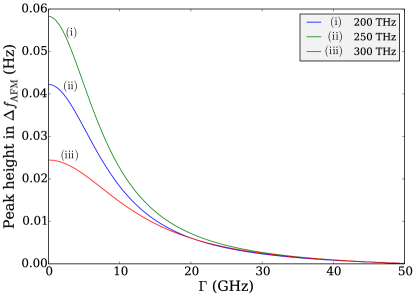
For a Rabi frequency exactly equal to the decoherence rate, the peak height is about 40% of its predicted decoherence-free value. Note that the plots in (c) are predicted to be applicable at low temperature (4K), while (a) and (b) could be used at higher temperatures if the decoherence rates go up. As our proposed experiment is to take place at temperatures of 4 K and higher, a Rabi frequency of 10 GHz seems sufficient to capture these decoherence signatures in the low temperature regime. This corresponds to an applied laser intensity of about 2 W/m2. Note however that an even smaller laser intensity (2 W/m2) is sufficient if one does not seek decoherence measurements, but only the native tunneling rates of the qubit.
Experimentally, the limiting factors in measuring these peaks are the (horizontal) resolution in the voltage on the biasing electrodes, and the (vertical) resolution in the frequency shift of the AFM. In practice, measured resonant peaks can be compared with model curves to yield information about the decoherence rates. For a sufficiently weak MIR field, the full-width-at-half-maximum height of each peak directly yields the decoherence rate. Even if the coupling strength between the MIR field and the DBP- is unknown, the decoherence rate can still be determined by extracting the resonant peak height as a function of width for various values of the power of the incident MIR field.Barrett and Stace (2006)
Fig. 11 conveys three key points of our proposal: how the tunneling rate can be inferred, how the decoherence model can be tested, and how the decoherence rate is obtained if the model is correct. The tunneling rate is revealed by observing resonances of the AFM frequency shift and is obtained by choosing and judiciously. The decoherence model is tested by seeing whether the frequency shift obeys the model-predicted dependence on driving-field frequency and static bias. Finally, the decoherence rate is obtained by comparing the measured resonance peak heights with those predicted for a decoherence-free system. The plots in Fig. 12 serve as examples of expected behavior and can be used in practice for extracting decoherence parameters from experimental data.
In the spin-boson decoherence model discussed here, the decoherence rate can be determined solely from the width of the peak because and are equal up to second order in the limit of weak qubit-bath coupling. For a noise model with independent relaxation and dephasing rates, Eq. (42) demonstrates sensitivity to changes in each of these rates independently.
A practical concern in performing the experiment is the back-action of our detector (AFM) on the quantum system being measured. The AFM cantilever has a frequency of Hz, whereas the oscillation frequency of the dangling-bond excess-charge is estimated to be Hz. Thus, the AFM tip motion looks adiabatic to the excess charge and the back-action of the tip on coherent electron dynamics in the dangling-bond pair is negligible.
There is, however, a static component of the tip perturbation on the qubit, which is the flipside of the AFM sensitivity of charge location: the tip creates a static bias along the DBP- axis. We calculated this bias for our optimized setup to have a maximum of 15.8 meV at the spatial location of maximum AFM sensitivity. Fortunately, this static bias does not significantly alter our scheme as it just adds to the applied static bias, and the resonance peaks will still be obtained albeit with a horizontal shift of 15.8 meV. Therefore, correcting for this back-action is just a simple matter of recalibrating the horizontal () axis in our plots so the peak locations become again symmetric. Thus we have the ability to measure this shift and compensate for it in any subsequent data processing.
VII Summary and conclusion
We have proposed a feasible experimental scheme for characterizing the fast tunneling rate as well as the nature and rate of decoherence of an excess charge shared between a pair of coupled dangling-bonds on the surface of silicon. In our scheme, the electrostatic potential across the dangling-bond pair is ramped by external electrodes. Furthermore the dangling-bond pair is driven by a MIR field, and the resulting resonances correspond to equal distribution of the electron location in the dangling-bond pair despite, and independent of, the strength of the static bias thereby revealing the desired tunneling properties.
The distribution of the excess electron between left and right dangling bonds is detected by capacitively coupling the DB excess charge to an atomic force microscope tip. Resonances are observed on the AFM frequency-shift signal when the MIR field matches the ramped tunneling frequency of the excess charge.
Experimentally, charge qubit geometries must be chosen so that tunnel splittings (and corresponding driving frequencies) should avoid undesired excitations such as the different vibration modes of H-Si bondsLucovsky et al. (1979); Lucovsky (1979) in the interval from 526 to 1111 cm-1. In practice, a control experiment would first be used to calibrate the AFM probe in the absence of driving radiation. In order to calibrate the vertical oscillation frequency as a function of lateral position, an AFM tip will be placed at different positions near a single DB-. The AFM vertical oscillation frequency will exhibit a shift that depends on the lateral position of the tip with respect to the charge and the tip height. Oscillation amplitudes and tip height can then be adjusted to obtain maximum signal.
Our scheme will enable in-depth studies of quantum coherent transport of electrons between dangling bonds on the surface of silicon and enable the study of phonons and other interactions. As dangling bond systems are promising building blocks for quantum-level engineering of novel devices including quantum-dot cellular automataHaider et al. (2009) and quantum computing,Livadaru et al. (2010) a detailed quantitative analysis of electron dynamics in dangling bond assemblies is an important step.
Acknowledgements.
We greatly appreciate valuable discussions with S. D. Barrett and T. M. Stace. This project has been supported by NSERC, AITF, and CIFAR.References
- Nakamura et al. (1999) Y. Nakamura, Y. A. Pashkin, and J. S. Tsai, Nature (London) 398, 786 (1999).
- Hollenberg et al. (2004) L. C. L. Hollenberg, A. S. Dzurak, C. Wellard, A. R. Hamilton, D. J. Reilly, G. J. Milburn, and R. G. Clark, Phys. Rev. B 69, 113301 (2004).
- Hayashi et al. (2003) T. Hayashi, T. Fujisawa, H. D. Cheong, Y. H. Jeong, and Y. Hirayama, Phys. Rev. Lett. 91, 226804 (2003).
- Gorman et al. (2005) J. Gorman, D. G. Hasko, and D. A. Williams, Phys. Rev. Lett. 95, 090502 (2005).
- Elzerman et al. (2004) J. M. Elzerman, R. Hanson, L. H. Willems van Beveren, B. Witkamp, L. M. K. Vandersypen, and L. P. Kouwenhoven, Nature (London) 430, 431 (2004).
- Schofield et al. (2013) S. Schofield, P. Studer, C. Hirjibehedin, N. Curson, G. Aeppli, and D. Bowler, Nat. Commun. 4, 1649 (2013).
- Wallraff et al. (2005) A. Wallraff, D. I. Schuster, A. Blais, L. Frunzio, J. Majer, M. H. Devoret, S. M. Girvin, and R. J. Schoelkopf, Phys. Rev. Lett. 95, 060501 (2005).
- Haider et al. (2009) M. B. Haider, J. L. Pitters, G. A. DiLabio, L. Livadaru, J. Y. Mutus, and R. A. Wolkow, Phys. Rev. Lett. 102, 046805 (2009).
- Livadaru et al. (2010) L. Livadaru, P. Xue, Z. Shaterzadeh-Yazdi, G. A. DiLabio, J. Mutus, J. L. Pitters, B. C. Sanders, and R. A. Wolkow, New J. Phys. 12, 083018 (2010).
- Pitters et al. (2011a) J. L. Pitters, L. Livadaru, M. B. Haider, and R. A. Wolkow, J. Chem. Phys. 134, 1 (2011a).
- Gardner et al. (2011) J. Gardner, S. D. Bennett, and A. A. Clerk, Phys. Rev. B 84, 205316 (2011).
- Petta et al. (2004) J. R. Petta, A. C. Johnson, C. M. Marcus, M. P. Hanson, and A. C. Gossard, Phys. Rev. Lett. 93, 186802 (2004).
- Stace et al. (2005) T. M. Stace, A. C. Doherty, and S. D. Barrett, Phys. Rev. Lett. 95, 106801 (2005).
- Zhu et al. (2005) J. Zhu, M. Brink, and P. L. McEuen, Appl. Phys. Lett. 87, 242102 (2005).
- Cockins et al. (2010) L. Cockins, Y. Miyahara, S. D. Bennett, A. A. Clerk, S. Studenikin, P. Poole, A. Sachrajda, and P. Grutter, Proc. Nat. Acad. Sci. U.S.A 107, 9496 (2010).
- Cockins et al. (2012) L. Cockins, Y. Miyahara, S. D. Bennett, A. A. Clerk, and P. Grutter, Nano Lett. 12, 709 (2012).
- Giessibl (2003) F. J. Giessibl, Rev. Mod. Phys. 75, 949 (2003).
- Fuechsle et al. (2012) M. Fuechsle, J. A. Miwa, S. Mahapatra, H. Ryu, S. Lee, O. Warschkow, L. C. L. Hollenberg, G. Klimeck, and M. Y. Simmons, Nat. Nanotechnol. 7, 242 (2012).
- Zikovsky et al. (2011) J. Zikovsky, S. A. Dogel, M. H. Salomons, J. L. Pitters, G. A. DiLabio, and R. A. Wolkow, J. Chem. Phys. 134, 114707 (2011).
- Pitters et al. (2011b) J. L. Pitters, I. A. Dogel, and R. A. Wolkow, ACS Nano 5, 1984 (2011b).
- Tong and Wolkow (2006) X. Tong and R. A. Wolkow, Surf. Sci. 600, L199 (2006).
- Thoms and Butler (1995) B. D. Thoms and J. E. Butler, Surf. Sci. 328, 291 (1995).
- Buehler and Boland (2000) E. J. Buehler and J. J. Boland, Science 290, 506 (2000).
- McEllistrem et al. (1998) M. McEllistrem, M. Allgeier, and J. J. Boland, Science 279, 545 (1998).
- Hitosugi et al. (1999) T. Hitosugi, S. Heike, T. Onogi, T. Hashizume, S. Watanabe, Z.-Q. Li, K. Ohno, Y. Kawazoe, T. Hasegawa, and K. Kitazawa, Phys. Rev. Lett. 82, 4034 (1999).
- van der Wiel et al. (2002) W. G. van der Wiel, S. De Franceschi, J. M. Elzerman, T. Fujisawa, S. Tarucha, and L. P. Kouwenhoven, Rev. Mod. Phys. 75, 1 (2002).
- Curl and Tittel (2002) R. F. Curl and F. K. Tittel, Annu. Rep. Prog. Chem, Sect. C: Phys. Chem 98, 219 (2002).
- Allen and Eberly (1975) L. Allen and J. H. Eberly, Optical Resonance and Two-Level Atoms (John Wiley and Sons, New York, 1975).
- Barrett and Stace (2006) S. D. Barrett and T. M. Stace, Phys. Rev. Lett. 96, 017405 (2006).
- Raghunathan et al. (2006) V. Raghunathan, R. Shori, O. M. Stafsudd, and B. Jalili, phys. stat. sol. (a) 203, R38 (2006).
- Schwalb et al. (2007) C. Schwalb, M. Lawrenz, M. Dürr, and U. Höfer, Physical Review B 75, 085439 (2007).
- Carslaw and Jaeger (1959) H. S. Carslaw and J. C. Jaeger, Conduction of Heat in Solids (Oxford University Press, Oxford, 1959), 2nd ed.
- Gross et al. (2007) L. Gross, L. Bourgouin, A. J. Hale, and H.-B. Muhlhaus, Phys. Earth Planet. Inter. 163, 23 (2007).
- Palik (1985) E. D. Palik, ed., Handbook of Optical Constants of Solids, vol. 1 (Academic Press, San Diego, 1985), ISBN 0125444206.
- Spitzer and Fan (1957) W. Spitzer and H. Y. Fan, Physical Review 108, 268 (1957).
- Cockins et al. (2009) L. Cockins, Y. Miyahara, and P. Grutter, Phys. Rev. B 79, 121309 (2009).
- Stomp et al. (2005) R. Stomp, Y. Miyahara, S. Schaer, Q. Sun, H. Guo, P. Grutter, S. Studenikin, P. Poole, and A. Sachrajda, Phys. Rev. Lett. 94, 056802 (2005).
- Marchi et al. (2008) F. Marchi, R. Dianoux, H. J. H. Smilde, P. Mur, F. Comin, and J. Chevrier, J. Electrostat. 66, 538 (2008).
- Morita et al. (2009) S. Morita, F. J. Giessibl, and R. Wiesendanger, eds., Noncontact Atomic Force Microscopy (Springer-Verlag, Berlin, 2009).
- Gross et al. (2009) L. Gross, F. Mohn, P. Liljeroth, J. Repp, F. J. Giessibl, and G. Meyer, Science 324, 1428 (2009).
- Schneiderbauer et al. (2012) M. Schneiderbauer, D. Wastl, and F. J. Giessibl, Beilstein J. Nanotechnol. 3, 174 (2012).
- Kobayashi et al. (2011) K. Kobayashi, H. Yamada, and K. Matsushige, Rev. Sci. Instrum. 82, 033702 (2011).
- Rezeq et al. (2006) M. Rezeq, J. Pitters, and R. A. Wolkow, J. Chem. Phys. 124, 204716 (2006).
- Feenstra (2003) R. M. Feenstra, J. Vac. Sci. Technol. B 21, 2080 (2003).
- Kantorovich et al. (2000) L. N. Kantorovich, A. I. Livshits, and M. Stoneham, J. Phys.: Condens. Matter 12, 795 (2000).
- Giessibl (1997) F. J. Giessibl, Phys. Rev. B 56, 16010 (1997).
- Caldeira and Leggett (1981) A. O. Caldeira and A. J. Leggett, Phys. Rev. Lett. 46, 211 (1981).
- Lindblad (1976) G. Lindblad, Comm. Math. Phys. 48, 119 (1976).
- Lucovsky et al. (1979) G. Lucovsky, R. Nemanich, and J. Knights, Physical Review B 19, 2064 (1979).
- Lucovsky (1979) G. Lucovsky, Journal of Vacuum Science and Technology 16, 1225 (1979).