Version: March 14, 2024
Giant Secondary Grain Growth in Cu Films on Sapphire
Abstract
Single crystal metal films on insulating substrates are attractive for microelectronics and other applications, but they are difficult to achieve on macroscopic length scales. The conventional approach to obtaining such films is epitaxial growth at high temperature using slow deposition in ultrahigh vacuum conditions. Here we describe a different approach: sputter deposition at modest temperatures followed by annealing to induce secondary grain growth. We show that polycrystalline as-deposited Cu on -Al2O3(0001) can be transformed into Cu(111) with centimeter-sized grains. Employing optical microscopy, x-ray diffraction, and electron backscatter diffraction to characterize the films before and after annealing, we find a particular as-deposited grain structure that promotes the growth of giant grains upon annealing. To demonstrate one potential application of such films, we grow graphene by chemical vapor deposition on wafers of annealed Cu and obtain epitaxial graphene grains of 0.2 mm diameter.
Vapor-phase thin film deposition, first enabled by the invention of modern vacuum technology about a century ago Mattox:2003uq , has developed into an essential component of many modern technologies. Advances in electron diffraction and microscopy over the past century provided tools for probing the crystalline structure of thin films and spurred investigation of the fundamental processes that determine grain size and orientation Pashley:1975kx . Thus grain growth and epitaxy have become central topics in thin film research. In applications of thin films, much effort is spent manipulating grain structure to achieve specific mechanical, electrical, magnetic, optical, and chemical properties. Examples include magnetic recording media Piramanayagam:2007fk , electrochemical catalysts Vliet:2012ys , and interconnects for microelectronics whose resistance to electromigration depends on film texture and grain size Tan:2007uq . A common challenge for metals and semiconductors grown on insulating substrates is to obtain a desired orientation of grains (such as <111> perpendicular to the film plane) along with macroscopic grain sizes ( in the plane of the film). The conventional approach to this challenge to is to seek conditions that produce large epitaxial grains during growth. An alternative approach, and the one that is the focus of this work, is to deposit a polycrystalline film and then produce large epitaxial grains by annealing. Although the basic idea was clearly described almost 25 years ago by C. V. Thompson et al., who called it “epitaxial grain growth” Thompson:1990kx , it has remained relatively unexplored since then. Here we show that this approach can produce films with individual grains with area .
The work described here was motivated by a desire to produce Cu(111) films that approach the ideal of a single crystal and that are suitable as substrates for chemical vapor deposition (CVD) of graphene and hexagonal boron nitride (h-BN) at temperatures near . Copper is the most commonly used substrate for graphene CVD because its negligible carbon solubility enables growth of precisely one layer over a wide range of growth conditions. It can also be readily etched away to allow transfer of the graphene to other substrates for further device fabrication steps Suk:2011vn . Although polycrystalline Cu foils are typically used, the Cu(111) surface provides a hexagonal template with a relatively small lattice mismatch (3.8% and 2.2% for graphene and h-BN, respectively) that allows epitaxial growth with low, uniform strain He:2012fk . Previous work on bulk single crystals has shown that graphene has less rotational disorder when grown on Cu(111) than on Cu(100) Nie:2011ys ; Wofford:2010fk . Exploiting the benefits of Cu(111) for commercial, wafer-scale production of graphene will require a process for producing crystalline films on a suitable substrate. A particularly attractive substrate is -Al2O3(0001). It is widely used by manufacturers of radio-frequency electronics and light-emitting diodes in the form of wafers with diameters up to 200 mm, it is physically and chemically stable under graphene CVD conditions, and it can likely be reused after metal etching to release the graphene layer.
There is a large body of work pertaining to Cu on -Al2O3, which is a model system for epitaxy, adhesion, and other properties of metal-ceramic interfaces Dehm:2005fk . On the -Al2O3(0001) surface, Cu grows epitaxially with a (111) texture, i.e. ||, and with two distinct in-plane orientation relationships (ORs). The most commonly observed OR (typically referred to as OR I) is ||. The second OR, called OR II, is ||. The two ORs differ by a rotation of about <111>. Several studies have found that the dominant OR depends sensitively on substrate preparation Scheu:2006bh ; Oh:2006zr ; Oh:2007fk , substrate temperature Dehm:2005fk , deposition rate Dehm:2005fk , and other conditions Curiotto:2011zr . We show here that a particular mixture of OR I and OR II in as-deposited Cu films enables giant grain growth upon annealing.
Grain growth in thin films can occur during deposition and during subsequent processing steps such as annealing Thompson:2000fr . The equilibrium state of a film is determined by the interplay of various energies: film-substrate interface, film free surface, grain boundary, and strain. The actual state of a film is also affected by kinetic processes such as diffusion, thus substrate temperature and the energy of arriving species during deposition are important in determining grain size and orientation. Due to the interplay among various energies, conventional grain growth stagnates when the average grain size is about the film thickness Thompson:2000fr . In some cases, particularly for Cu and other fcc metals where grain boundaries are mobile at relatively low temperatures, grains can grow larger than the stagnation limit through a process known as secondary grain growth Thompson:1985mz . This occurs when grains of a particular low energy orientation grow at the expense of a matrix of other, stagnated grains. Although secondary grain growth can occur during deposition, it is typically exploited during subsequent annealing Thompson:1990kx , as we do here. In Cu films sputtered onto amorphous SiO2, secondary grain growth driven by minimization of strain energy has produced grains to across with a (100) orientation Takewaki:1995fk ; Vanstreels:2008fj . In our epitaxial Cu films, the fact that a (111) orientation is favored indicates surface and interface energies dominate over strain energies Thompson:2000fr ; Deng:2012kx .
Annealing can cause a thin film to break into discontinuous islands, a phenomenon known as dewetting or agglomeration Thompson:2012fk ; Srolovitz:1995kx . The process, which is driven by minimization of the total energy of the film/substrate system, typically begins with the development of thermal grooves at grain boundaries in the film Mullins:1957fk . These grooves deepen at a rate that increases with temperature, and dewetting occurs when the grooves reach the substrate, so thinner films become discontinuous at lower temperatures. For films exposed to temperatures near the bulk melting point, as is the case when Cu (melting point of ) is used for CVD of graphene, dewetting is a major limitation on the survivability of the film. Fortunately, grain growth and dewetting are competing processes Thompson:2000fr . As we show here, the growth of giant grains at temperatures somewhat below allows Cu films to endure subsequent graphene growth conditions with minimal dewetting.
In this paper, we present an extensive investigation of grain size and orientation for Cu films sputtered onto -Al2O3(0001) substrates at a wide range of temperatures, and then annealed at temperatures near . We characterize our films using x-ray diffraction (XRD) and electron backscatter diffraction (EBSD) to measure crystallinity, and optical microscopy to show film properties over large areas. We also report results for large domain graphene growth by CVD on these films, characterized by optical microscopy and Raman spectroscopy. Our findings show that an appropriate combination of deposition and annealing temperatures can produce Cu(111) single crystal films, free of twinning and thermal grooves, over macroscopic length scales. Such films offer an ideal substrate for epitaxial CVD of graphene, h-BN, and possibly other materials.
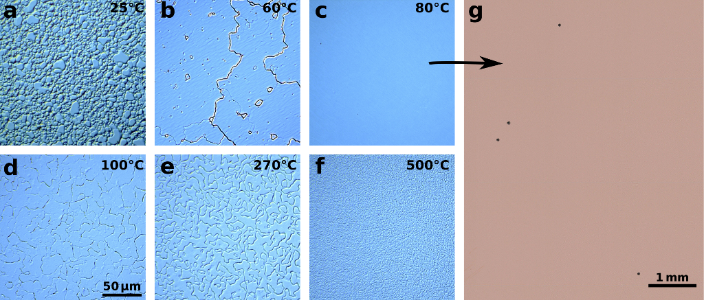
Figure 1 shows optical microscopy images of Cu films deposited at various temperatures and annealed at temperature for 40 min. The annealing conditions were chosen to be similar to those used for graphene CVD, but without the hydrocarbon precursor (see Methods). Images for additional values of and are shown in Supplementary Fig. S1. The dark lines apparent in Fig. 1b,d,e are thermal grooves that mark the edges of grain boundaries in the Cu film (see Miller:2012fk and Supplementary Fig. S2 for confirmation of this correspondence). Since these films are 450 nm thick, conventional grain growth stagnation would limit grains to roughly the film thickness, or . The actual grains are much larger than this limit, and for the grains exceed the image size. Figure 1g shows a larger area from a wafer, and the absence of thermal grooves in this image indicates there are no grain boundaries over the entire area. (See Supplementary Fig. S3 for EBSD maps of the rare grain boundaries that remain after annealing.) The dark spots in Fig. 1g are areas of dewetting, likely due to microscopic particles introduced during transfer between deposition and annealing steps. Examination of such films with the naked eye shows the Cu grains are typically across. We have observed such giant grain growth on several 50 mm wafers with .
It is evident from Fig. 1 that giant grain growth only occurs for a narrow range of near . In order to understand the conditions that lead to giant grain growth, we have examined the structure of the Cu films at various using XRD before and after annealing. The XRD results for the as-deposited films, Figs. 2a-c, reveal a sudden, qualitative change in film properties as increases. For , we observe: (1) a small (100) component to the film texture (Fig. 2a, note log scale), (2) broad tails in the rocking curve, which measures misalignment of the <111> vector (Fig. 2b), and (3) peaks corresponding to both OR I and OR II in the azimuthal scan (Fig. 2c). The peaks every instead of in the azimuthal scans indicate both OR I and OR II consist of twins that are related by an in-plane rotation of . This twinning, which is expected because the OR between a (111) cubic film and a hexagonal substrate is equivalent for a in-plane rotation, has limited the crystallinity of Cu(111) in several graphene CVD studies Miller:2012fk ; Reddy:2011kx ; Ishihara:2011kx ; Hu:2012vn . For , the film texture is purely (111), the rocking curve has no tails, and the azimuthal scan shows a single OR. The changes in these three features point to a sudden transition to improved epitaxy between and . Surprisingly, it is just below this transition where giant grain growth is most pronounced, i.e., better as-deposited epitaxy does not necessarily promote giant grain growth upon annealing.
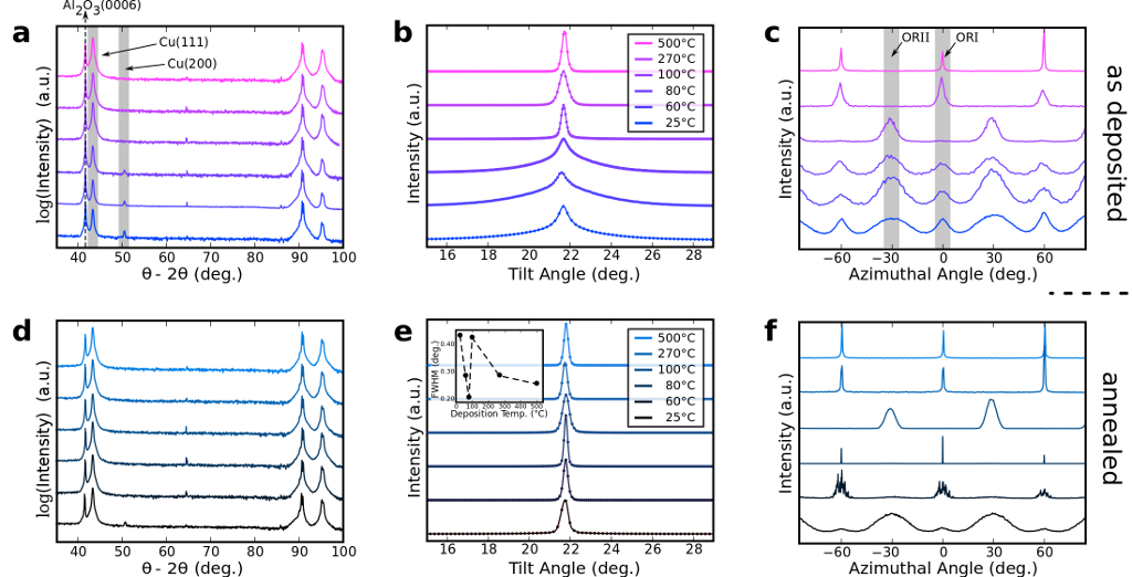
The XRD results for the annealed films, Figs. 2d-f, show that annealing decreases polycrystallinity for all films: the (100) component is reduced, the rocking curve tails for are eliminated, and the azimuthal scans show a clear preference for one OR in all cases. The width of the rocking curve peak (inset of Fig. 2e) shows a sharp minimum at the value of for which giant grain growth is most pronounced. The azimuthal scan for the film shows a complete absence of OR II grains, with sharp peaks at the OR I directions whose width matches the instrumental limit set by beam divergence (see Methods). The azimuthal scan for the film shows clusters of sharp peaks, indicating the presence of a few large grains with discrete orientations near the nominal OR I direction.
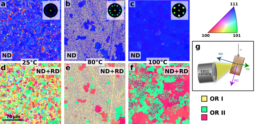
The XRD results point to a specific polycrystalline state of the as-deposited film that favors giant grain growth. We have used EBSD to study the microstructure of the Cu grains in this polycrystalline state. Texture maps for = , and are shown in Fig. 3a-f. The geometry of the EBSD measurement, with definitions of reference, transverse and normal directions (RD, TD, and ND), is shown in Fig. 3g. Figures 3a-c show ND maps, which indicate the out-of-plane direction according to the color scale defined at the right side of the figure, with a (111) pole figure as an inset to each map. Figures 3d-f show ND+RD maps where the in-plane component highlights the distinction between OR I and OR II, as shown by the colored squares at the right side of the figure. (For this choice of map, the OR II twins appear as two different colors but both OR I twins appear as a single color.) These maps show a microstucture that is consistent with the XRD results for the corresponding in Figs. 2a-c. For , the as-deposited film is mostly (111) with a small (100) component that appears as a few red grains in the ND map in Fig. 3a. The multiple shades of blue in the ND map indicate many grains are somewhat misaligned from (111), which is consistent with the broad XRD rocking curve tails. Both the pole figure and the ND+RD map (Fig. 3d) show grains distributed broadly near OR I and OR II in roughly equal proportion. For , only grains close to (111) appear in the ND map (Fig. 3c), and the ND+RD map shows only OR II grains (Fig. 3f). For , which favors giant grain growth upon annealing, the as-deposited film is marked by a nonuniform distribution of grain sizes: the ND map in Fig. 3b shows several (111) grains that are much larger than their neighbors, and the ND+RD map in Fig. 3e shows that these large grains are exclusively OR II. The pole figure has 12 spots due to twinning in both the OR II grains (pink and green in Fig. 3e) and in the smaller OR I grains (yellow in Fig. 3e). The variation of colors for OR II grains is due to in-plane misalignment about the nominal epitaxial direction of up to several degrees. This is consistent with the broad OR II peaks in the XRD azimuthal scans in Fig. 2c.
Although the large grain size for OR II in Fig. 3e indicates OR II is favored over OR I during deposition, the XRD data of Fig. 2f show the OR II grains are completely converted into OR I grains during annealing. This suggests the energy difference between OR I and OR II is small and changes sign as temperature is increased. Indeed, previous studies point to the same conclusion: ab initio, zero temperature calculations Hashibon:2005uq found OR I and OR II differ by 3%, with OR II favored, whereas measurements of the shape of individual Cu particles created by solid-state dewetting at indicate a 4% difference with OR I favored Curiotto:2011zr . The different in-plane strain expected for the two ORs, tensile for OR I and compressive for OR II Hashibon:2005uq , is qualitatively consistent with this finding: since Cu expands more rapidly than -Al2O3(0001) as temperature increases, the strain energy of an OR under tensile strain will decrease and that of an OR under compressive strain will increase.
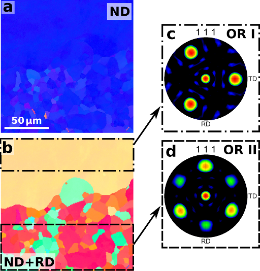
To examine the intermediate stages of giant grain growth, we used shorter annealing times and lower annealing temperatures. For a film annealed for at , we found exclusively OR II grains (Supplementary Fig. S4). After annealing for 20 min at , we found individual OR I grains starting to consume the surrounding matrix of OR II grains (Supplementary Fig. S2). Figure 4 shows the boundary between a giant OR I grain and the matrix for a film annealed at for 40 min, i.e., as grain growth is nearing completion. Separate pole figures for the upper and lower regions, Figs. 4c,d, show that the upper region is a single OR I grain (no twinning) whereas the matrix contains both OR II twins. It is clear that the process of giant grain growth involves OR I grains consuming OR II grains upon annealing. In order for this to occur, the as-deposited film must contain a fraction of both orientation relationships, because if there are no OR I seed grains present (as is the case with ) or if the film is already exclusively OR I (), the film will stagnate with the as-deposited orientation relationship, creating thermal grooves between twins and eventually severe dewetting (Supplementary Fig. S1). Deposition at provides a mix of grain orientations that promotes growth of giant OR I grains before significant dewetting occurs, thus stabilizing the Cu film and allowing it to survive graphene CVD conditions. Annealing of a film deposited through a shadow mask to create isolated Cu islands showed the density of OR I seed grains is only about one per mm2 (Supplementary Fig. S6).
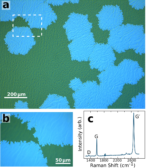
Graphene grown by CVD (see Methods) is shown in Fig. 5. We have optimized the growth parameters for large graphene domains and growth on thin films. Notably, we use an Ar overpressure of () to suppress Cu sublimation and maintain thin film stability. The image in Fig. 5a was taken after stopping growth before a complete graphene layer formed. The sample was baked in air at for 5 min to oxidize the bare Cu regions and thus provide optical contrast with unoxidized regions covered by graphene. The graphene islands are roughly 6-fold symmetric, as expected for a Cu(111) surface, and are across. Supplementary Fig. S7 contains additional images of graphene grown on giant Cu grains. The graphene domains appear to be aligned, suggesting epitaxy and consistent with other results Hu:2012vn . Since the Cu is epitaxial with the sapphire substrate, this enables alignment of macroscopic features such as sample edges with zig-zag and armchair directions in graphene nanostructures. Figure 5b shows the dendritic nature of the island perimeter. This type of growth is similar to graphene growth at low pressures where the H2/CH4 ratio is close to 1. Figure 5c is a Raman spectrum of the graphene after transfering a continuous graphene film to a 300 nm oxidized Si substrate using PMMA and thermal release tape. The IG’/IG peak ratio is 2.3, with Lorentzian FWHM peak widths of 12 cm-1 and 27 cm-1 for the G and G’ peaks, respectively, and the D peak is small. All these features indicate a high quality, monolayer graphene film.
We have demonstrated a route to single crystal Cu(111) films over centimeter length scales based on dramatic secondary grain growth of a favored orientation of Cu on -Al2O3(0001). Our XRD and EBSD results show in detail the particular as-deposited grain structure that promotes giant grain growth upon annealing. Although this work has focused on Cu films thick enough to survive graphene CVD conditions, we expect similar phenomena to occur at lower temperatures for thinner films, based on standard grain growth models. Furthermore, materials other than Cu should also be suitable for giant grain growth if the required as-deposited grain structure can be obtained. A promising candidate is Al on -Al2O3(0001), since films having a mixture of OR I and OR II have already been demonstrated Dehm:2005fk .
Methods
Cu film deposition and annealing.
Wafers of crystalline -Al2O3(0001), 50 mm in diameter, were annealed at in O2 at atmospheric pressure for 24 h to remove scratches due to polishing and give atomically flat terraces. Without further processing, wafers were mounted on a resistively heated Cu puck and placed in a vacuum sputter deposition system. Films of 450 nm nominal thickness were deposited by dc magnetron sputtering from 76 mm targets of 99.999% pure Cu at a rate of . Actual film thickness measured using a profilometer ranged from 430 nm to 500 nm across the wafer, but this variation had no discernable effect on the results. Films with were deposited in a load-locked, turbopumped chamber (base pressure ) with a target-to-substrate distance of and a sputtering power of in of Ar. Films deposited at were deposited in a cryopumped bell-jar-style chamber (base pressure ) with a target-to-substrate distance of and a sputtering power of in of Ar. The deposition temperature reported here was measured using a thermometer in contact with the sample puck. After deposition, each wafer was coated with PMMA and diced into chips. The chips were stripped of PMMA and cleaned by ultrasonic agitation in acetone and isopropanol before characterization and annealing. Annealing was performed in a hot-wall tube furnace with a base pressure of at temperatures ranging from to for a duration of 40 min. The temperature of the furnace was measured using a thermocouple mounted just outside the quartz tube. To suppress Cu sublimation, we maintained a total pressure of while flowing 500 sccm 99.999% pure Ar and 11 sccm of 0.2% H2 in Ar, yielding a H2 partial pressure of .
XRD and EBSD.
X-ray diffraction was performed using a Cu Kα source and a 4-circle goniometer with an instrument resolution of . All measurements were performed using parallel beam optics with a maximum beam divergence of , which sets the minimum rocking curve linewidth achievable in the experiment. A powder Si sample was used to correct any offsets in the angle. Symmetric scans were used to determine the out-of-plane crystalline axes. Once the (111) reflection was found, the tilt angle was scanned to generate the (111) rocking curve. In-plane azimuthal scans of the (220) reflection were taken with the grazing incidence angle adjusted to the value of maximum intensity (typically about above the critical angle). At this angle, the entire sample is illuminated by the x-rays. Once the (220) peak was located, an azimuthal scan about the sample normal axis was taken to determine the in-plane angular distribution of the [220] axes.
For EBSD measurements, all films were oriented with parallel to the RD direction. The SEM accelerating voltage was 20 kV, the chip was tilted towards the detector, and diffraction patterns were collected with 4 4 binning over a hexagonal array of 500 nm pixels.
Graphene growth, transfer, and characterization.
Before graphene growth, the Cu was annealed at for 1 h under 69.5 sccm of 0.2% H2 in Ar to form large grains that are less susceptible to dewetting at higher temperatures. The flow of 0.2% H2 in Ar was then decreased to 11 sccm, giving a H2 partial pressure of , and the temperature was ramped to and stabilized for 5 min. Growth was initiated by introducing 14 sccm of 0.2% CH4 in Ar, yielding a CH4 partial pressure of . Growth conditions were maintained for 40 min to achieve complete monolayer coverage over an entire chip or wafer. Partial growths were achieved by reducing the growth time. All gases were filtered at the mass flow controller inlets to remove H2O and O2 contaminants to . For transfer of graphene to oxidized Si, PMMA was spun onto the surface and baked at , and thermal release tape was applied to the PMMA. Chips were floated on the surface of an ammonium persulfate bath overnight to etch away the Cu. The Al2O3 substrate fell away, leaving the graphene/PMMA/tape layer on the liquid surface, and this was then rinsed in DI water and placed on a Si chip with of SiO2. The Si chip was heated to on a hot plate to release the tape, and then to to soften the PMMA and promote adhesion of graphene to the SiO2 Suk:2011vn . To remove the PMMA layer, the chips were submerged in glacial acetic acid for several hours at room temperature. Raman spectroscopy was performed using an excitation wavelength of 532 nm.
References
- (1) Mattox, D. The Foundations of Vacuum Coating Technology (William Andrew Publishing, 2003).
- (2) Pashley, D. W. A historical review of epitaxy. In Matthews, J. W. (ed.) Epitaxial Growth, Part A (Academic Press, 1975).
- (3) Piramanayagam, S. N. Perpendicular recording media for hard disk drives. J. Appl. Phys. 102, 011301 (2007).
- (4) van der Vliet, D. F. et al. Mesostructured thin films as electrocatalysts with tunable composition and surface morphology. Nature Materials 11, 1051–1058 (2012).
- (5) Tan, C. M. & Roy, A. Electromigration in ULSI interconnects. Mater. Sci. Engin. Rep. 58, 1 – 75 (2007).
- (6) Thompson, C. V., Floro, J. & Smith, H. I. Epitaxial grain growth in thin metal films. J. Appl. Phys. 67, 4099–4104 (1990).
- (7) Suk, J. W. et al. Transfer of CVD-grown monolayer graphene onto arbitrary substrates. ACS Nano 5, 6916–6924 (2011).
- (8) He, R. et al. Large physisorption strain in chemical vapor deposition of graphene on copper substrates. Nano Lett. 12, 2408–2413 (2012).
- (9) Nie, S., Wofford, J. M., Bartelt, N. C., Dubon, O. D. & McCarty, K. F. Origin of the mosaicity in graphene grown on Cu(111). Phys. Rev. B 84, 155425 (2011).
- (10) Wofford, J. M., Nie, S., McCarty, K. F., Bartelt, N. C. & Dubon, O. D. Graphene islands on Cu foils: The interplay between shape, orientation, and defects. Nano Lett. 10, 4890–4896 (2010).
- (11) Dehm, G., Edongué, H., Wagner, T., Oh, S. & Arzt, E. Obtaining different orientation relationships for Cu films grown on (0001) -Al2O3 substrates by magnetron sputtering. Inter. J. Mat. Res. 96, 249–254 (2005).
- (12) Scheu, C. et al. Bonding at copper–alumina interfaces established by different surface treatments: a critical review. J. Mater. Sci. 41, 5161–5168 (2006).
- (13) Oh, S. H., Scheu, C., Wagner, T., Tchernychova, E. & Rühle, M. Epitaxy and bonding of Cu films on oxygen-terminated -Al2O3(0001) surfaces. Acta Materialia 54, 2685 – 2696 (2006).
- (14) Oh, S. H., Scheu, C., Wagner, T. & Rühle, M. Control of bonding and epitaxy at copper/sapphire interface. Appl. Phys. Lett. 91, 141912 (2007).
- (15) Curiotto, S. et al. Orientation relationships of copper crystals on c-plane sapphire. Acta Materialia 59, 5320 – 5331 (2011).
- (16) Thompson, C. V. Structural evolution during processing of polycrystalline thin films. Annu. Rev. Mater. Sci. 30, 159–190 (2000).
- (17) Thompson, C. V. Secondary grain growth in thin films of semiconductors: Theoretical aspects. J. Appl. Phys. 58, 763–772 (1985).
- (18) Takewaki, T., Yamada, H., Shibata, T., Ohmi, T. & Nitta, T. Formation of giant-grain copper interconnects by a low-energy ion bombardment process for high-speed ULSIs. Mater. Chem. Phys. 41, 182 – 191 (1995). URL http://www.sciencedirect.com/science/article/pii/0254058495015124.
- (19) Vanstreels, K. et al. Increasing the mean grain size in copper films and features. J. Mater. Res. 23, 642–662 (2008). URL http://dx.doi.org/10.1557/JMR.2008.0080.
- (20) Deng, J. Phase field modeling of grain growth in thin films on rigid substrates. Phys. Stat. Sol. B 249, 564–574 (2012).
- (21) Thompson, C. V. Solid-state dewetting of thin films. Annu. Rev. Mater. Res. 42, 399–434 (2012).
- (22) Srolovitz, D. & Goldiner, M. The thermodynamics and kinetics of film agglomeration. JOM 47, 31–36 (1995).
- (23) Mullins, W. W. Theory of thermal grooving. J. Appl. Phys. 28, 333–339 (1957).
- (24) Miller, D. L., Keller, M. W., Shaw, J. M., Chiaramonti, A. N. & Keller, R. R. Epitaxial (111) films of Cu, Ni, and CuxNiy on - Al2O3 (0001) for graphene growth by chemical vapor deposition. J. Appl. Phys. 112, 064317 (2012).
- (25) Reddy, K. M., Gledhill, A. D., Chen, C.-H., Drexler, J. M. & Padture, N. P. High quality, transferrable graphene grown on single crystal Cu(111) thin films on basal-plane sapphire. Appl. Phys. Lett. 98, 113117 (2011).
- (26) Ishihara, M., Koga, Y., Kim, J., Tsugawa, K. & Hasegawa, M. Direct evidence of advantage of Cu(111) for graphene synthesis by using Raman mapping and electron backscatter diffraction. Mater. Lett. 65, 2864 – 2867 (2011).
- (27) Hu, B. et al. Epitaxial growth of large-area single-layer graphene over Cu(111)/sapphire by atmospheric pressure CVD. Carbon 50, 57 – 65 (2012).
- (28) Hashibon, A., Elsässer, C. & Rühle, M. Structure at abrupt copper–alumina interfaces: An ab initio study. Acta Materialia 53, 5323 – 5332 (2005).
Acknowledgements
The authors thank Carl Thompson for helpful discussions of grain growth phenomena. Optical microscope images were taken in NIST’s Precision Imaging Facility.
Author contributions
D.L.M. and M.W.K. designed the experiments, built custom equipment, and performed film deposition. J.M.S. performed XRD measurements and data analysis. K.P.R., R.R.K., and D.L.M. performed EBSD measurements and analysis. D.L.M. and K.M.D. performed annealing, optical microscopy, graphene growth, and graphene transfer. D.L.M. performed Raman spectroscopy. M.W.K. and D.L.M. wrote the manuscript. All authors discussed the data and commented on the manuscript.
Additional information
The authors declare no competing financial interests. Supplementary information accompanies this paper on www.nature.com/naturematerials. Reprints and permissions information is available online at http://npg.nature.com/reprintsandpermissions. Correspondence and requests for materials should be addressed to M.W.K.