McMillan-Rowell Oscillations in a Low Spin-Orbit SNS Semiconducting Junction
Abstract
The electronic transport properties of an SNS junction formed by an InN nanowire (N) and Al contacts (S) with a superconducting transition temperature T K were investigated. As a function of dc bias, superconducting quasiparticle transport resonance peaks at were observed, in agreement with BCS theory with 2=275eV. Several additional transport resonances scaling linearly in energy were observed at high-bias above 2, up to , consistent with McMillan-Rowell oscillations. The persistence of McMillan-Rowell oscillations at high-bias and under applied magnetic field were investigated.
pacs:
74.45.+c,73.23.-b, 73.63.-b,There has been recent intense interest in the properties of hybrid structures composed of a low-dimensional semiconductor coupled by proximity effect to superconducting metal contactsYJDohDelft ; RFrielinghaus ; TNishioKoji ; Spathis . Following seminal theoretical work proposing the existence of engineered Majorana fermions in proximity-coupled strong spin-orbit semiconductor devices FuKane ; JSauQW ; JAlicea ; JSauNW , recent reports have shown encouraging experimental evidence for zero-energy Majorana modesVMourikDelft ; ADasHeiblum ; LRokhinson . To observe Majorana modes, these studies have focused on large spin-orbit semiconductors such as InAs or InSb, and little attention has been devoted to similar devices fabricated with low spin-orbit material such as InN. We report here an extensive study of an SNS junction fabricated from an InN nanowire grown by molecular beam epitaxy (MBE). In addition to a zero-bias anomaly, non-linear transport resonances are clearly observed at bias energies up to fifteen times the superconducting gap . These resonances are consistent with McMillan-Rowell oscillations (MRO) Rowell within the semiconducting nanowire. The persistence of MRO at high bias implies the persistence of Andreev reflection to high bias energy, suggesting that Andreev reflection at the semiconductor - superconductor interface is not fully understood.
The density of states, energy gap and Fermi velocity of a superconductor can be determined experimentally by tunnelling spectroscopy. This is usually achieved in an ideal SN junction by measuring the differential resistance or conductance as a function of dc bias energy applied across the barrier. Generalized Andreev reflection in SNS tunnel junctions was described theoretically by Blonder, Tinkham, and Klapwijk (BTK)BTK ; Tinkham and has been successfully used to explain the tunnelling spectroscopy of junctions with a normal metal tunnelling barrier. However, in the case where a semiconductor takes the place of a normal metal, the band gap in the semiconductor density of states will modify the junction properties. In particular, the breakdown of the Andreev approximation will modify the Andreev reflection probability at the interface.
We performed electron transport measurements on devices made with InN nanowires coupled to Al leads. The devices were fabricated from nearly intrinsic (not intentionally doped) non-tapered InN nanowires grown on Si (111) substrates by a Veeco Gen-II radio frequency plasma-assisted MBE growth system. Photoluminescent and XPS measurements show a band gap of approximately 0.675 eV and minimal surface charge effect on the nanowires Mi1 ; Mi2 . The wire length is 0.9 m and the diameter of the investigated nanowire is 120 nm. The -axis is along the nanowire growth direction. To fabricate the ohmic contacts, the wires were transferred from the original (as-grown) substrate to an Si(100) wafer with a 100 nm thick SiO2 insulating layer. Transfer was accomplished by diluting nanowires into an acetone solution in an ultrasonic bath, followed by drop casting the solution onto the target substrate. The substrate was pre-patterned with a mark array by photolithography to locate and identify each individual nanowire by scanning electron microscopy (SEM). Contact electrodes of Ti(10 nm)/Al(100 nm) were deposited by e-beam evaporation and lithography to establish superconducting contacts to the InN nanowires. An SEM image of a representative device is shown in the inset of Fig. 1 (a), as well as the as-grown nanowires. Electrical transport measurements were performed in a dilution refrigerator equipped with a 9 T magnet down to temperatures of 23 mK. Magnetoresistance was measured by a constant-current source and a low-frequency ac and dc current bias technique. The differential resistance dependence on source-drain voltage was obtained by a lock-in technique with an ac current of = 50 nA, and the differential conductance was found by numerical inversion. In all data show in this work, a contact resistance was subtracted.
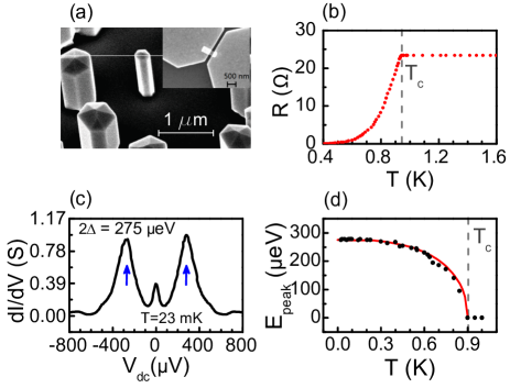
The contacts to the junction were verified to be ohmic. The two-point resistance was found to be less than 25 in the normal state. Nanowires grown under the same conditions have been measured to give two-point resistances on the order of 1 M in high-vacuum scanning probe experiments Mi3 . We attribute the discrepancy in resistance to electron doping of the nanowire. InN has a very high electron affinity (5.8 eV Ager ), and will thus be electron doped by the Al contacts and also possibly by surface contaminants introduced during lithography and wet processing. The temperature dependence of the resistance was determined from 0.3 to 150 K, and is shown in Fig.1 (b) in the range between 0.4 K and 1.6 K. The abrupt drop in resistance at 0.92 K is consistent with previous work based on superconducting aluminum thin films. The coherence length of the Al contact nm, assuming a diffusion coefficient for aluminum , which is of order of the Al contact separation. From the Fermi velovity in the nanowire, we estimate a temperature length at 1K, suggesting that our junction is always in the mesocopic regime.
The differential conductance measured by applying a mixed dc and ac current through the superconducting contacts is plotted in Fig.1 (c) at T = 23 mK. Quasiparticle (QP) resonant peaks at = 275 eV are observed symmetrically in vs at both positive and negative biases. A conductance peak at zero bias is observed, whose origin is presently unknown and requires further investigation. Measurements of the spectra dependence on were performed at several temperatures from 23 mK to 1 K. The QP peak position versus temperature is shown in Fig.1(d), fitting well to a BCS theory of the gapTinkham indicated by the red line. The QP peak energy at can be inferred from the BCS fit, from which we find eV. Our measurement is consistent with the expected BCS gap 2eV Tinkham determined from the superconducting transition temperature K of Fig. 1 (b). The InN nanowire junction thus behaves consistently within weak-coupling BCS theory.
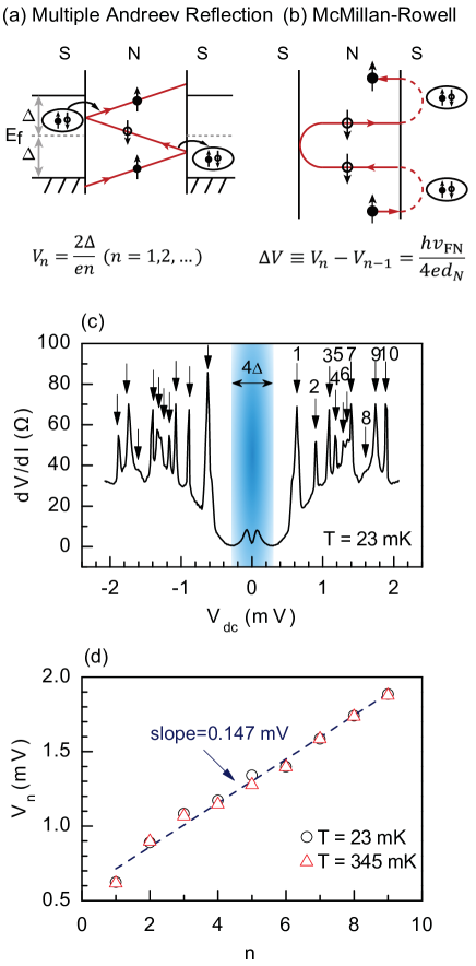
In addition to superconducting QP peaks at 2 = 0.275 meV, numerous other transport resonances are observed in at bias energies above 2 as shown in Fig. 2(c). The resonances beyond 2 are enumerated by , and the resonant bias voltage is plotted versus in Fig. 2(d) at 23 mK and 345 mK. A clear linear increase in resonant bias is observed with a slope 0.1470.007 mV, with a noticeable deviation occurring at . Notably, as the temperature is increased the resonances weaken in amplitude and eventually disappear as . This suggests that these features are directly related to a transport mechanism directly tied to the superconducting gap, implying important contributions from Andreev reflections.
We now turn to an interpretation of the transport resonances above the BCS gap. At temperatures below the superconducting transition temperature , transport resonances can occur due to Andreev reflection at SN interfaces. Multiple Andreev reflection (MAR) shown schematically in Fig. 2(a) results in transport resonances at sub-gap energies , where is the interference order. MAR is expected to be strong in SNS junctions where the transparency of each SN interface is similar, and greatly suppressed in junctions with significant SN interface asymmetry. Sub-gap transport resonances are notably absent in the InN nanowire junction, as seen in Fig. 2(c). On the other hand, MRO ONesher ; Rowell ; WJGallagher ; Ingerman are transport resonances that can occur in an asymmetric SNS junction, resulting from normal reflections at the opaque SN interface and Andreev reflection at the transparent SN interface, depicted in Fig. 2(b). The reflections establish a series of geometrical resonances leading to MRO, and were first observed by direct measurement of density of states. MRO also manifests itself in a series of equidistant peaks in the dynamic transport spectrum,
| (1) |
where is the Fermi velocity in the normal material, and is the effective length of the normal region of the junction. Note that contrary to the typical situation of an SNS junction with a metallic normal region, the Fermi velocity of a semiconducting normal region is tuneable with carrier density, and the Fermi energy much smaller. As shown in Fig. 2(b), the transport resonances in our SNS junction are observed to be equidistant, scaling linearly with with a slight deviation at , in good agreement with MRO. The clear observation of these sharp and well-defined MROs suggest a ballistic transport occurring in the nanowire. The slope of versus and the nanowire length together with Eq. 1 allows us to estimate an electron Fermi velocity in the InN nanowire of cm/s. Furthermore, assuming a three-dimensional density of states for the relatively large diameter nanowire we infer an electron density of order of . This density agrees within an order of magnitude with previous measurements using an electrical nanoprobing techniqueMi3 . Taking the effective mass of InN as , the corresponding Fermi energy is estimated to be above the conduction band edge. The ratio of Fermi energy to the superconducting gap is , which is several orders of magnitude smaller than can be typically achieved in an SNS junction with a metallic normal region. Importantly, BTK theory of the SNS junction is valid in the limit , a valid approximation for metallic normal regions but which is expected to break down for junctions with semiconducting normal regions of low carrier density. A surprising feature of the transport resonances is the persistence in resonance amplitude up to an energy of , in contradiction with the expected rapid collapse of Andreev reflection probability (less than ) at large bias in SNS junctions with metallic normal regions BTK . The persistence of MRO to high bias has however been experimentally observed in previous work with cuprates, up to energies ten times the superconducting gap ONesher .
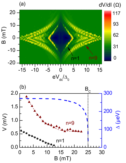
The persistence of MRO was further investigated in the presence of a magnetic field applied perpendicular to the substrate and nanowire. The measured is shown in Fig. 3 (a) as a two-dimensional contour plot of versus / over magnetic field ranging from 22.5 mT to -20.5 mT. The central dark diamond shaped region of low resistivity includes the QP peaks in (dips in ). The QP resonances disappear with applied magnetic field, as expected from the weakening of the BCS gap under magnetic field. The MRO peaks in , indicated by bright lines, evolve with magnetic field and eventually disappear at a critical field, thereby recovering the fully linear character of electron transport. The evolution of the first and last observed MRO peak, and , is plotted versus in Fig. 3 (b). For comparison, the scaling of the BCS gap with magnetic field is also illustrated by a dotted line. Although all features are seen to disappear at a critical field, the dispersion of and versus differ with each other and with the trend of the weak-coupled BCS gap. The dispersion in threshold may arise from a variety of magnetic field induced effects, such as the modulation of the coherence length , modulation of Andreev reflection probability, and magnetic confinement. Further experimental and theoretical work is required to better understand the magnetic field behaviour of low spin-orbit InN SNS junctions.
In conclusion, we have investigated the transport properties of a hybrid SNS device formed with a low spin-orbit InN nanowire. The sharp, non-linear transport resonances observed at energies well above the superconducting gap are attributed to MRO, and are amongst the most pronounced observations of MRO in electrical transport. The persistence of MRO to biases well above gap suggest that Andreev reflection at interfaces of semiconductors and conventional s-wave superconductors persist to high energies unlike the collapse of Andreev reflection probability at high bias at an interface of normal metal and semiconductor. The observed persistence and dispersion of MRO, and thus Andreev reflection, in an SNS junction with semiconducting normal region is presently not understood. In order to realize devices from heterostructures composed of semiconductor / superconductor junctions, further work is required to understand the nature of basic electron transport phenomena. In particular, an extension of BTK theory to account for situations of small Fermi energy may be required to describe Andreev processes in weakly doped semiconductors.
We thank S. Bohloul, H. Guo and A. Clerk for stimulating discussions. We acknowledge the technical assistance of Richard Talbot, Robert Gagnon and John Smeros. This work was supported by NSERC (Canada), FRQNT (Québec), and CIFAR. We also thank the McGill Nanotools Microfabrication Facility.
References
- (1) Y.J. Doh, J. A. van Dam, A. L. Roest, E. P. A. M. Bakkers, L. P. Kouwenhoven, and S. De Franceschi, Science, 309, 272, (2005).
- (2) R. Frielinghaus, I. E. Batov, M. Weides, H. Kohlstedt, R. Calarco and Th. Schäpers, Appl. Phys. Lett., 96, 132504, (2010).
- (3) T. Nishio, T. Kozakai, S. Amaha, M. Larsson, H. A. Nilsson, H. Q. Xu, G. Zhang, K. Tateno, H. Takayanagi, and K. Ishibashi, Nanotechnol., 22, 445701, (2011).
- (4) P. Spathis, S. Biswas, S. Roddaro, L. Sorba, F. Giazotto, and F. Beltram, Nanotechnol., 22, 105201, (2011).
- (5) L. Fu and C. L. Kane, Phys. Rev. Lett., 100, 096407, (2008).
- (6) J. D. Sau, R. M. Lutchyn, S. Tewari, and S. Das Sarma, Phys. Rev. Lett., 104, 040502, (2010).
- (7) J. Alicea, Phys. Rev. B, 81, 125318, (2010).
- (8) J. D. Sau, S. Tewari, R. M. Lutchyn, T. D. Stanescu, and S. Das Sarma, Phys. Rev. B, 82, 214509, (2010).
- (9) V. Mourik, K. Zuo, S. M. Frolov, S. R. Plissard, E. P. A. M. Bakkers, and L. P. Kouwenhoven, Science, 336, 1003, (2012).
- (10) A. Das, Y. Ronen, Y. Most, Y. Oreg, M. Heiblum, and H. Shtrikman, Nat. Phys., 8, 887, (2012).
- (11) L. P. Rokhinson, X. Liu, and J. K. Furdyna, Nat. Phys., 8, 795, (2012).
- (12) J. M. Rowell and W. L. Mcmillan, Phys. Rev. Lett., 16, 453, (1966).
- (13) G. E. Blonder, M. Tinkham, and T. M. Klapwijk, Phys. Rev. B, 25, 4515, (1982).
- (14) M. Tinkham, Introduction to Superconductivity, Second Edition, Dover Publications, 1996.
- (15) Y. L. Chang, Z. Mi, and F. Li, Adv. Funct. Mater. 20, 4146, (2010).
- (16) S. Zhao, S. Fathololoumi, K. H. Bevan, D. P. Liu, M. G. Kibria, Q. Li, G. T. Wang, Hong Guo, and Zetian Mi, Nano lett., 12, 2877, (2012).
- (17) S. Zhao, O. Salehzadeh, S. Alagha, K. L. Kavanagh, S. P. Watkins, and Z. Mi, Appl. Phys. Lett., 102, 073102, (2013).
- (18) J. W. Ager III, N. Miller, R. E. Jones, K. M. Yu, J. Wu, W. J. Schaff and W. Walukiewicz, phys. stat. sol. (b) 245, 873 (2008).
- (19) O. Nesher and G. Koren, Phys. Rev. B, 60, 9287, (1999).
- (20) W. J. Gallagher, Phys. Rev. B, 22, 1233, (1980).
- (21) Å. Ingerman, G. Johansson, V. S. Shumeiko, and G. Wendin, Phys. Rev. B, 64, 144504, (2001).