Double injection in graphene p-i-n structures
Abstract
We study the processes of the electron and hole injection (double injection) into the i-region of graphene-layer and multiple graphene-layer p-i-n structures at the forward bias voltages. The hydrodynamic equations governing the electron and hole transport in graphene coupled with the two-dimensional Poisson equation are employed. Using analytical and numerical solutions of the equations of the model, we calculate the band edge profile, the spatial distributions of the quasi-Fermi energies, carrier density and velocity, and the current-voltage characteristics. In particular, we demonstrated that the electron and hole collisions can strongly affect these distributions. The obtained results can be used for the realization and optimization of graphene-based injection terahertz and infrared lasers.
I Introduction
Due to unique properties, graphene-layer (GL) and multiple-graphene-layer (MGL) structures 1 with p-n and p-i-n junctions are considered as novel building blocks for a variety of electron, terahertz, and optoelectronic devices. Such junctions have been realized using both chemical doping 2 ; 3 ; 4 ; 5 ; 6 and ”electrical” doping in the gated structures 7 ; 8 ; 9 ; 10 . The formation of p-n and p-i-n junctions with the electrically induced p- and n-regions is possible even in MGL structures with rather large number of GLs 11 . Different devices based on p-i-n junctions in GL and MGL structures have been proposed recently. In particular, the GL and MGL structures with reversed biased p-i-n junctions can be used in infrared (IR) and terahertz (THz) detectors 12 ; 13 ; 14 ; 15 ; 16 ; 17 ; 18 ; 19 and the tunneling transit-time THz oscillators 20 ; 21 . The GL and MGL p-i-n junctions under the forward bias can be the basis of IR and THz lasers exploiting the interband population inversion 22 ; 23 ; 24 ; 25 (see also recent experimental results, 26 ; 27 ; 28 ), in which the injection of electrons and holes from the n- and p-regions is utilized 29 ; 30 instead of optical pumping. A simplified model of the GL and MGL injection lasers with the p-i-n junctions was considered recently 30 . The model in question assumes that the recombination of electrons and holes in the i-region and the leakage thermionic and tunneling currents at the p-i and i-n interfaces are relatively small. This situation can occur in the structures with sufficiently short i-regions or at relatively low temperatures when the recombination associated with the emission of optical phonons and thermionic leakage are weakened. In such a case, different components of the current can be considered as perturbations, and the spatial distributions of the electric potential and the carrier density along the i-region are virtually uniform. However, in the p-i-n structures with relatively long i-regions and at the elevated voltages the spatial distribution of the potential can be rather nonuniform, particularly, near the edges of the i-region, i.e. near the p-i and i-n interfaces. In this case, the electric field in the i-region can be sufficiently strong. Such an effect can markedly influence the density of the injected carriers, the conditions of the population inversion and current-voltage characteristics.
In this paper, we develop a model for the GL and MGL forward biased p-i-n structures which accounts for relatively strong recombination and consider its effect on the characteristics which can be important for realization of IR/THz injection lasers. The problem of the electron and hole injection (double injection) in GL and MGL p-i-n structures is complicated by the two-dimensional geometry of the device and the features of the carrier transport properties. This makes necessary to use two-dimensional Poisson equation for the self-consistent electric potential around the i-region and to invoke the hydrodynamic equations for carrier transport in GL and MGLs. Thus, the present model is a substantial generalization of the model applied in the previous paper 30 . To highlight the effects of strong recombination and the nonuniformity of the potential distributions, we, in contrast to Ref. 30 ; 31 , disregard for simplicity the effects of the carrier heating or cooling and the effects associated with the nonequilibrium optical phonons. This can be justified by the fact that the injection of electrons and holes from the pertinent contacts does not bring a large energy to the electron-hole system in the i-region unless the applied bias voltage is large.
The paper is organized as follows. In Sec. II, we present the GL and MGL p-i-n structures under consideration and the device mathematical model. Section III deals with an analytical solutions of the equations of the model for a special case. Here the general equations are reduced to a simple equation for the quasi-Fermi energies of electrons and holes as functions of the applied bias voltage. In Sec. IV, the equations of the model are solved numerically for fairly general cases. The calculations in Secs. III and IV provide the spatial distributions of the band edges, the quasi-Fermi energies and densities of electrons and holes, and their average (hydrodynamic) velocities. It is shown, that the obtained analytical distributions match well with those obtained numerically, except very narrow regions near the p-i and i-n interfaces. In Sec. V, the obtained dependences are used for the calculation of the current-voltage characteristics of the GL and MGL p-i-n structures. Sec. VI deals with the discussions of some limitations of the model and possible consequences of their lifting. In Sec. VII we draw the main conclusions.
II Model
II.1 The structures under consideration
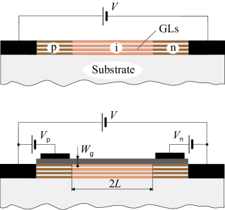
We consider the GL or MGL p-i-n structures with either chemically or electrically doped p- and n-region (see, the sketches of the structures on the upper and lower panels in Fig. 1). We assume that the p- and n-regions (called in the following p- and n-contacts) in single- or multiple-GL structures are strongly doped, so that the Fermi energy in each GL in these structures and hence, the built-in voltage are sufficiently large:
where is the temperature and is the Boltzmann constant. In the single-GL structures with the electrically induced p- and n-contact regions,
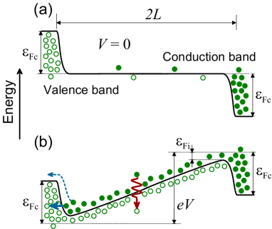
where and are the Planck constant and the dielectric constant, respectively, cm/s is the characteristic velocity of electrons and holes in GLs, is the gate layer thickness, and is the gate voltage ( and (see Fig. 1). Figure 2 shows the schematic views of the band profiles of a GL p-i-n structure at the equilibrium [see Fig. 2(a)] and at the forward bias [see Fig. 2(b)]. The Fermi energies of the holes and electrons in the contact p- and n-regions are assumed to be . It is shown that at , the densities of electron and hole (thermal) in the i-region are relatively small. But at the forward bias these density become rather large due to the injection. The injection is limited by the hole charge near the p-i junction and by the electron charge near the i-n junction. Due to this, the Fermi energy of the injected electrons and holes, , at the pertinent barriers is generally smaller than . However, at the bias voltages comparable with the build-in voltage , these Fermi energy can be close to each other. The qualitative band profiles of Fig. 2 are in line with the band profiles found from the self-consistent numerical calculation shown in Sec. IV.
Due to high electron and hole densities in the i-region under the injection conditions, the electron and hole energy distribution are characterized by the Fermi functions with the quasi-Fermi (counted from the Dirac point) and , respectively, and the common effective temperature , which is equal to the lattice temperature.
II.2 Equations of the model
The model under consideration is based on the two-dimensional Poisson equation for the self-consistent electric potential and the set of hydrodynamic equations describing the electron and hole transport along the GL (or GLs) in the i-region. The Poisson equation for the two-dimensional electric potential is presented as
| (1) |
where is the electron charge, and are the net electron and hole sheet densities in the system (generally consisting of GLs), and are the densities of donors and acceptors in the i-region (located primarily near the contact regions), and is the delta function reflecting the fact that the GL (MGL system) are located in a narrow layer near the plane . The axis is directed in this plane.
The transport of electrons and holes is governed by the following system of hydrodynamic equations 32 :
| (2) |
| (3) |
| (4) |
| (5) |
| (6) |
Here is the potential in the GL plane, , , , and are the quasi-Fermi energies and hydrodynamic velocities of electrons and holes, respectively, is the collision frequency of electrons and holes with impurities and acoustic phonons, is their collision frequency with each other, and is the fictitious mass, which at the Fermi energies of the same order of magnitude as the temperature can be considered as a constant. The recombination rate in the case of dominating optical phonon mechanism can be presented in the following simplified form (see, for instance, Refs. 30 ; 31 ; 33 :
| (7) |
Here is the equilibrium density of electrons and holes in the i-region in one GL at the temperature , is the characteristic time of electron-hole recombination associated with the emission of an optical phonon, is the rate of thermogeneration of the electron-hole pairs due to the absorption of optical phonons in GL at equilibrium, is the optical phonon energy, and .
II.3 Boundary conditions
The boundary conditions for the electron and hole velocities and Fermi energies are taken in the following form:
| (8) |
and
| (9) |
where is the spacing between p- and n-region (length of the i-region), is the recombination velocity of electrons and holes in narrow space-charge regions adjacent to the p- and n-region, respectively, due to the interband tunneling and due to the leakage over the barriers (edge recombination velocity) 7 ; 34 , and is the applied bias voltage (see Fig.1) . The quantity is the Fermi energy at the contact regions. The electric potential at the the contact regions is determined by the applied voltage :
| (10) |
| (11) |
where is the applied bias voltage. Combining Eqs. (9) - (11), one obtains
| (12) |
| (13) |
The dependence yields the coordinate dependence of the Dirac point or the band edge profile (with respect to its value in the i-region center, ).
II.4 Dimensionless equations and boundary conditions
To single out the characteristic parameters of the problem we introduce the following dimensionless variables: , , , , , , , , , , , , , and . Using these variables, Eqs. (1) (6) are presented as
| (14) |
| (15) |
| (16) |
| (17) |
| (18) |
| (19) |
| (20) |
Here and are the ”electrostatic” and ”diffusion” parameters given, respectively, by the following formulas:
Assuming, m, , , K, meV, s-1, s, we obtain , . The same values of one obtains if s -1 and s. The parameters and can also be presented as and , where and are the characteristic screening and the diffusion lengths in the i-region (in equilibrium when ), respectively, and is the diffusion coefficient.
The boundary conditions for the set of the dimensionless Eqs. (14) - (20) are given by
| (21) |
| (22) |
| (23) |
| (24) |
In the following we focus our consideration mainly on the structures with very abrupt p-i and i-p junction neglecting terms and in Eq. (14). The effect of smearing of these junctions resulting in and will be briefly discussed in Sec. VI.
III Injection characteristics (Analytical approach for a special case)
Consider the special case in which . When , Eq. (14) is actually a partial differential equation with a small parameter () at highest derivatives. Usually the net solution of such equations can be combined from their solutions disregarding the left side (valid in a wide range of independent variables) and the solution near the edges (which are affected by the boundary conditions) in the regions of width , where the derivatives are large, provided a proper matching of these solutions 35 . Hence, since parameter , for a wide portion of the i-region one can assume that and, consequently, .
In this case, Eqs. (15) and (16) yield
| (25) |
| (26) |
It is instructive that the condition , assumed above, is fulfilled only if the collisions with impurities and acoustic phonons are disregarded. Therefore, in this section we assume that . Considering this, we find
| (27) |
At the points , one can use the simplified matching conditions [see Fig. 2(b)] and obtain the following equation for :
| (28) |
or
| (29) |
If , one can expect that , so that , and Eq. (29) yields
| (30) |
At , (the electron and hole components are degenerate), from Eq. (29)
| (31) |
If formally (very long diffusion length or near ballistic transport of electrons and holes in the i-region), one can see from Eqs. (29) - (31) that tends to , i.e., the Fermi energies of electrons and holes tend to (as in the previous paper 30 ).
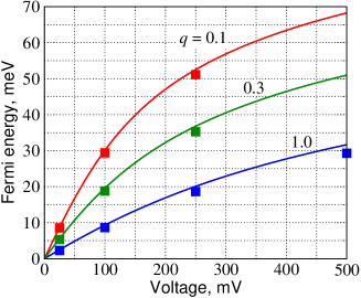
Figure 3 shows the voltage dependences of the Fermi energy, , of electrons and holes in the main part of the i-region calculated using Eq. (29) for different values of parameter . The dependences shown in Fig. 3 imply that the recombination leads to the natural decrease in the Fermi energies and the densities of electrons and holes in the i-region. These quantities increase with increasing applied voltage , but such an increase is a slower function of (logarithmic) than the linear one. The results of the calculations based on Eq. (29) (i.e., based on a simplified model valid for weak electron and hole collisions with impurities and acoustic phonons and the edge recombination) practically coincide with the results of numerical calculations involving a rigorous model (shown by the markers in Fig. 3). The results of these calculations are considered in the next Section.
IV Numerical results
Finding of analytical solutions of Eq. (14) coupled with Eqs. (15) - (20) in the near-edge region and their matching with the smooth solutions in the main portion of the i-region is a difficult problem due to the nonlinearity of these system of equations and its integro-differential nature. In principle, what could such solutions provide is an information on the width of the near-edge regions. The latter is not so important, because the main characteristics of the structures under consideration are determined by the electron-hole system in the structure bulk (in the main portion of the i-region). However, the net solution is particularly interesting to verify the results of the analytical model considered in Sec. III. For this purpose, we solved Eqs. (14) - (20) numerically by iterations.
Due to large values of parameter , one could expect very sharp behavior of and near the edges of the i-region, so that strongly nonuniform mesh was used. The potential was found by reducung the Poisson equation (14) to the following:
| (32) |
where
is the Green function, which corresponds to the geometry and the boundary conditions under consideration.
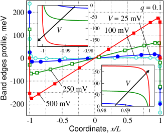
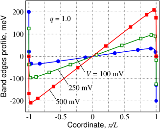
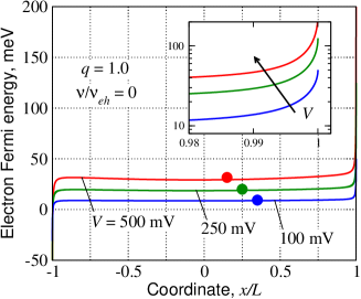
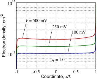
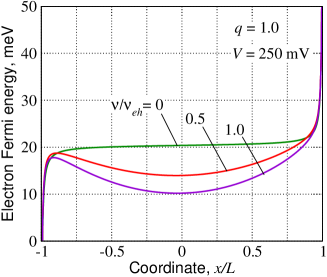
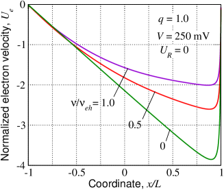
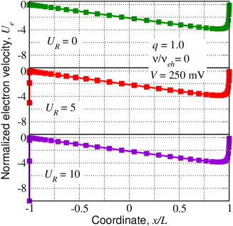
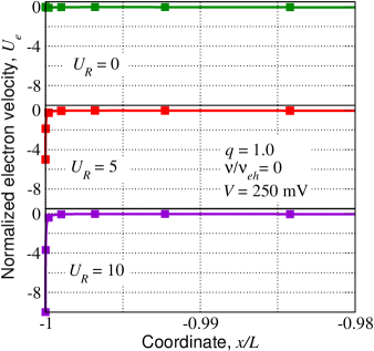
Figure 4 shows the profiles of the band edges, i.e.,the conduction band bottom (valence band top) in the i-region () obtained from numerical solutions of Eqs. (14) - (20) for different values of the bias voltage and parameter at (and as in Sec. III). As follows from Fig. 4, an increase in the bias voltage leads to the rise of the barrier for the electrons injected from the n-region and the holes from the p-region. These barriers are formed due to the electron and hole self-consistent surface charges localized in very narrow region (of the normalized width ) in the i-region near its edges. The electric field near the edges changes the sign. In the main portion of the i-region, the electric field is almost constant. Its value increases with increasing parameter , i.e., with reinforcement of the recombination. Figures 5 and 6 demonstrate the spatial distributions of the electron Fermi energy and the electron density in the i-region for at different bias voltages. The hole Fermi energy and the hole density are equal, respectively, to and .
One can see from Figs. 5 and 6 that the electron Fermi energy and the electron density steeply drop in fairly narrow region adjacent to the p-region. However, they remain virtually constant in the main portion of the i-region if the ratio of the collisions frequency of electrons and holes with impurities and acoustic phonons and the frequency of electron-hole collisions . In the latter case, the values of these quantities across almost the whole i-region coincide with those obtained analytically above with a high accuracy (see the markers in Figs. 3 and 5). This justifies the simplified approach used in the analytical model for the case developed in Sec. III. Nevertheless, at not too small values of parameter , the coordinate dependences of the electron (and hole) Fermi energy exhibit a pronounced sag (see Fig. 7). Similar sag was observed in the coordinate dependences of the electron and hole densities (not shown). As seen from Fig. 8, an increase in the ratio leads also to a pronounced modification of the coordinate dependences of the electron (hole) velocity: the absolute value of the electron velocity markedly decreases with increasing . However, the changes in the band edge profiles and, hence the electric field in the main portion of the i-region are insignificant.
Above, we have considered the cases of the p-i-n structures with sufficiently long i-region, so that the normalized edge recombination velocity . In such cases, in accordance with the boundary conditions (and tends to zero at the pertinent contact region (see Fig. 8).
The calculations of the spatial distributions of the band edge profiles, Fermi energies, and carrier concentrations showed that the variation of the edge recombination velocity (at least in the range from zero to ten) does not lead to any pronounced distinction even in the near-edge regions. In all cases considered, as seen from Fig. 9, the absolute value of steeply increases in a narrow region near the n-contact and the gradually drops (virtually linearly) across the main portion of the i-region. However, (and, hence, the electron hydrodynamic velocity ), being virtually independent of from the n-region to the near-edge region adjacent to the p-i interface, strongly depends on in the latter region [see Fig. 9 (both left and right panels)]. The hole velocity exhibits the same behavior with .
Due to rather short near-contact regions, the edge recombination does not affect substantially the integral characteristics of the p-i-n structures under consideration, in particular total number of the injected electrons and holes and their net recombination rate at least in the practical p-i-n structures with and not too large (i.e., not too short i-regions).
V Current-voltage characteristics
The current (associated with the recombination in the i-region) can be calculated as
| (33) |
Using the obtained analytical formulas derived above, in which , we find
| (34) |
or
| (35) |
where
| (36) |
Setting m and s at K, from Eq. (34) one obtains A/cm.
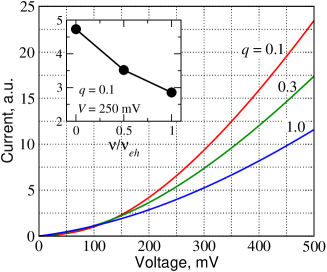
The current-voltage characteristics obtained for different parameters (using Eqs. (29) and (35) at ) are shown in Fig. 10. As follows from Fig. 10, the injection current superlinearly increases with increasing bias voltage . The steepness of such current-voltage characteristics decreases with increasing parameters . This is because a larger corresponds in part to larger , i.e, to a larger resistance. In the limit , the current-voltage dependence approaches to . Thus, at the transition from near ballistic electron ( and hole transport to collision dominated transport (), the current-voltage characteristics transform from exponential to superlinear ones.
However, at finite values of parameter , can be a prononced function of the coordinate as seen from Fig. 7. This results in a dependence of the current on the parameter in question. Inset in Fig. 10 shows the dependence of the current on parameter at fixed bias voltage. A decrease in the current with increasing parameter is associated with a sag in the spatial dependence of the Fermi energy (see Fig. 7), which gives rise to weaker recombination in an essential portion of the i-region and, therefore, lower recombination (injection) current.
VI Discussion
The rigorous calculation of the edge recombination current, particularly, its tunneling component and parameter requires special consideration. Here we restrict ourselves to rough estimates based of a phenomenological treatment. The characteristic velocity, , of the edge recombination due to tunneling of electrons through the barrier at the p-i-interface (and holes through the barrier at the i-n-interface) can be estimated as . Here is the effective barrier tunneling transparency, determined, first of all, by the shape of the barrier. The appearance of factor is associated with the spread in the directions of electron velocities in the GL plane. In the case of very sharp barrier, . But practically is less than unity, although due to the gapless energy spectrum of carriers in GLs and MGLs one can not expect that it is very small. The edge recombination velocity associated with the thermionic current of electrons (holes) over the pertinent barrier is proportional to , so that . The factor is very small when the contact n- and p-regions are sufficiently doped (), hence, . In the case of the electrically induced p- and n-regions in MGL structures, the condition can impose certain limitation on the number of GL 11 . As a result, parameter can be estimated as . At s, m, and we find that . As shown above, the edge recombination even at relatively large parameter markedly influences the carrier densities and their Fermi energies only in immediate vicinity of the p- and i-n interfaces (see Fig. 9). To find conditions when the surface (tunneling) recombination can be disregarded in comparison to the recombination assisted by optical phonons, we compare the contributions of this recombination to the net current. Taking into account Eq. (35) and considering that the edge recombination tunneling current , we obtain
| (37) |
Equation (37) yields the following condition when the edge recombination is provides relatively small contribution to the injection current:
| (38) |
Assuming that s, , and ( meV), from inequality (36) we obtain m. As follows from Eq. (38), the role of the edge recombination steeply drops when , i.e., the bias voltage increase. This is because the recombination rate , associated with optical phonons, rapidly rises with increasing . If s and ( meV), one can arrive at the following condition: m.
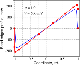
As demonstrated in Sec. IV, the spatial variations of the band edge profile, density of carriers and their Fermi energies are very sharp near the p-i and i-n interfaces. This is owing to large values of parameter and the assumption of abrupt doping profiles. In this case, the normalized width of the transition region is . In real GL and MGL p-i-n structures, the boundaries between p-, i-, and n-region are somewhat smeared (with the characteristic length ). This can be associated with the specifics of chemical doping or with the fringing effects. In the latter case, the length of the intermediate region is about the thickness of the gate layer (see Fig. 1). In both cases, this can result in a smoothing of the dependences in near-contact regions in comparison with those shown in Figs. 4 - 9 and in a marked decrease in the electric field in the p-i and i-p junctions and in the edge tunneling current. Figure 11 demonstrates examples of the band edge profiles calculated for the abrupt p-i and i-n junctions and for that with smeared junction. In the latter case, it was assumed that the acceptor and donor densities varied exponentially with the characteristic length : and , with , cm-2 (, ). As seen from Fig. 11, an increase in smearing of the dopant distributions leads to a natural increase in the widths of the transition regions and a decrease (relatively small) in the electrical field in the i-region.
At moderate number of GLs in the p-i-n structures under consideration, the net thickness of the latter , where nm is the spacing between GLs, is smaller than all other sizes. In such a case, the localization of the space charges of electrons and holes in the i-region in the -direction can be described by the delta function as in Eq. (1). In the case of large , the delta function should be replaced by a function with a finite localization width. This also should give rise to an extra smearing of the spatial distributions in the -direction. The pertinent limitation on the value can be presented as follows: , where is the screening length. At , assuming that and , one can obtain nm and arrive at the following condition . An increase in results in an increase in parameters and, hence, in some modification of the spatial distributions in near contact region, although the latter weakly affects these distributions in the main portion of the i-region. As a result, the injection current increases proportionally to (see Eq. (35)).
We disregarded possible heating (cooling) of the electron-hole system in the i-region. Under large bias voltages the electric field in this region can be fairly strong. In this case, the dependence of the drift electron and hole velocities on the electric field might be essential. However, relatively strong interaction of electrons and holes with optical phonons having fairly large energy prevents substantial heating 36 in the situations considered in the previous sections. Moreover, in the essentially bipolar system the recombination processes with the emission of large energy optical phonons provide a marked cooling of the system, so that its effective temperature can become even lower than the lattice temperature 30 ; 31 .
The above consideration was focused on the double injection in GL and MG p-in structures at the room temperatures. The obtained results are also applicable at somewhat lower temperatures if the recombination is primarily associated with optical phonons. However, at lower temperatures, other recombination mechanisms can become more crucial, for instance, the Auger recombination mediated by scattering mechanisms on impurities and acoustic phonons and due to trigonal warping of the GL band structure, which provide additional momentum and enables transitions to a broader range of final states 37 ; 38 ; 39 , i.e., the indirect Auger recombination 40 (see also Refs. 41 ; 42 ), acoustic phonon recombination, invoking the momentum transfer due to disorder 43 , radiative recombination 44 , tunneling recombination in the electron-hole puddles 45 and edge tunneling recombination (see Ref. 34 and Sec. IV). Relatively weak role of the optical phonon assisted processes at low temperatures can result in pronounced hot carrier effects (see, for instance, Refs. 46 ; 47 ). However, these effects are beyond the scope of our paper and require special consideration.
VII Conclusions
We studied theoretically the double electron-hole injection in GL and MGL p-i-n structures at the forward bias voltages using the developed device model. The mathematical part of the model was based on a system of hydrodynamic equations governing the electron and hole transport in GLs coupled with the two-dimensional Poisson equation. The model is characterized primarily by the following two parameters: the electrostatic parameter and the diffusion parameter . Large value of parameter in practical structures results in the formation of very narrow edge regions near p-i and i-n interfaces, in which all physical quantities vary sharply, and the formation of a wide region, which is stretched across the main portion of the i-region, where all spatial dependences are rather smooth. Using analytical and numerical solutions of the equations of the model, we calculated the band edge profiles, the spatial distributions of the quasi-Fermi energies, carrier density and velocity, and the current-voltage characteristics. It was demonstrated that the electron-hole collisions and the collisions of electrons and holes with impurities and acoustic phonons can strongly affect the characteristics of the p-i-n structures. In particular, such collisions result in a pronounced lowering of the injection efficiency (weaker dependences of the electron and hole Fermi energies and their densities on the bias voltage) and the modification of the current-voltage characteristics from an exponential to superlinear characteristics (at collision-dominated transport). It is also shown that for the case of relatively perfect GL and MGL structures, the developed analytical model provides sufficient accuracy in the calculations of spatial distributions in the main portion of the i-region and of the p-i-n structure overall characteristics. The effects associated with the edge recombination and smearing of the p-i and i-n junctions are evaluated.
The obtained results appear to be useful for the realization and optimization of GL- and MGL -based injection terahertz and infrared lasers.
Acknowledgments
The authors are grateful to M. S. Shur and V. Mitin for numerous fruitful discussions. The work was financially supported in part by the Japan Science and Technology Agency, CREST and by the Japan Society for Promotion of Science.
References
- (1) A. H. Castro Neto, F. Guinea, N. M.R. Peres, K. S. Novoselov, and A. K. Geim, REv. Mod Phys. 81, 109 (2009).
- (2) D. Farmer, Y.-M. Lin, A. Afzali-Ardakani, and P. Avouris, Appl. Phys. Lett. 94, 213106 (2009).
- (3) E. C. Peters, E. J. H. Lee, M. Burghard, and Klaus Kern, Appl. Phys. Lett. 97, 193102 (2010).
- (4) K. Yan, Di Wu, H. Peng, Li Jin, Q. Fu, X. Bao, and Zh. Liu, Nat. Comm. 3, 1280 (2012).
- (5) H. C. Cheng, R. J. Shiue, C. C. Tsai, W. H. Wang, Y. T. Chen, ACS Nano 5, 2051 (2011).
- (6) Yu Tianhua, C. Kim, C.-W. Liang, Yu Bin, Electron Device Lett. 32, 1050 (2011).
- (7) V. V. Cheianov and V. I. Falko, Phys. Rev. B 74, 041403 (2006).
- (8) B. Huard, J. A. Silpizio, N. Stander, K. Todd, B. Yang, and D. Goldhaber-Gordon, Phys. Rev. Lett. 98, 236803 (2007).
- (9) J. R. Williams, L. DiCarlo, and C.M. Marcus, Science 317, 638 (2007).
- (10) H-Y Chiu, V. Perebeinos, Y.-M. Lin, and P. Avouris, Nano Lett. 10, 4634 (2010).
- (11) M. Ryzhii, V. Ryzhii, T. Otsuji, V. Mitin, and M. S. Shur, Phys. Rev. B 82, 075419 (2010).
- (12) F. Xia, T. Mueller, Y.-M. Lin, A. Valdes-Garcia, and P. Avoris, Nature Nanotech, 4, 839 (2009).
- (13) V. Ryzhii, M. Ryzhii, V. Mitin, and T. Otsuji, J. Appl. Phys. 107, 054512 (2010).
- (14) T. Mueler, F. Xia, and P. Avouris, Nature Photon. 4, 297 (2010).
- (15) M. Ryzhii, T. Otsuji, V. Mitin, and V.Ryzhii, Jpn. J. Appl. Phys. 50, 070117 (2011).
- (16) N. M. Gabor, J. C. W. Song, Q. Ma, N. L. Nair, T. Taychatanapat, K. Watanabe, T. Taniguchi, L. S. Levitov, and P. Jarillo-Herrero Science, 334, 648 (2011).
- (17) V. Ryzhii, N. Ryabova, M. Ryzhii, N. V. Baryshnikov, V. E. Karasik, V. Mitin. and T. Otsuji, Optoelectronics Rev. 20, 15 (2012).
- (18) D. Sun, G. Aivazian, A. M. Jones, J. Ross, W. Yao, D. Cobden, X. Xu, Nature Nanotechnology 7, 114 (2012)
- (19) M. Freitag, T. Low, and P. Avouris, Nano Lett. 13 , 1644 (2013).
- (20) V. Ryzhii, M. Ryzhii, M. S. Shur, and V. Mitin, Appl. Phys. Express 2, 034503 (2009).
- (21) V. L. Semenenko, V. G. Leiman, A. V. Arsenin, V. Mitin, M. Ryzhii, T. Otsuji,and V. Ryzhii, J. Appl. Phys. 113, 024503 (2013).
- (22) V. Ryzhii, M. Ryzhii, and T. Otsuji, J. Appl. Phys. 101, 083114 (2007).
- (23) V. Ryzhii, M. Ryzhii, A. Satou, T. Otsuji, A. A. Dubinov, and V. Ya. Aleshkin, J. Appl. Phys. 106, 084507 (2009).
- (24) V. Ryzhii, A. A. Dubinov, T. Otsuji, V. Mitin, and M. S. Shur, J. Appl. Phys. 107, 054505 (2010).
- (25) A. A. Dubinov, V. Ya. Aleshkin, V. Mitin, T. Otsuji, and V. Ryzhii, J. Phys.: Condens. Matter 23, 145302 (2011).
- (26) S. Boubanga-Tombet, S. Chan, A. Satou, T. Otsuji, and V. Ryzhii Phys. Rev. B 85, 035443 (2012).
- (27) T.Otsuji, S. Boubanga-Tombet, A. Satou, M.Ryzhii, and V.Ryzhii, J. Phys. D 45, 303001 (2012).
- (28) T. Li, L. Luo, M. Hupalo, J. Zhang, M. C. Tringides, J. Schmalian, and J. Wang, Phys. Rev. Lett. 108, 167401 (2012).
- (29) M. Ryzhii and V. Ryzhii, Jpn. J. Appl. Phys. 46, L151 (2007).
- (30) V. Ryzhii, M. Ryzhii, V. Mitin, and T. Otsuji, J. Appl.Phys. 110, 094503 (2011).
- (31) V. Ryzhii, M. Ryzhii, V. Mitin, A. Satou, and T. Otsuji, Jpn. J. Appl. Phys. 50, 094001 (2011).
- (32) D. Svintsov, V. Vyurkov, S. O. Yurchenko, T. Otsuji, and V. Ryzhii, J. Appl. Phys. 111, 083715 (2012).
- (33) F. Rana, P. A. George, J. H. Strait, J. Dawlaty, S. Shivaraman, M. Chandrashekhar, and M. G. Spencer Phys. Rev. B 79, 115447 (2009).
- (34) V. Ryzhii, M. Ryzhii, and T. Otsuji, Phys. Stat. Sol. (a) 205, 1527 (2008).
- (35) Ali H. Nayfeh Perturbation Methods (WILEY-VCH, Weinheim, 2004).
- (36) R. S. Shishir and D. K. Ferry, J. Phys. Condens. Matter 21, 344201 (2009).
- (37) M. S. Foster and I. Aleiner, Phys. Rev. B 79, 085415 (2009).
- (38) L. E. Golub, S. A. Tarasenko, M. V. Entin, and L. I. Magarill, Phys. Rev. B 84, 195408 (2011).
- (39) A. Satou, V. Ryzhii, Y. Kurita, and T. Otsuji, J. Appl. Phys. 113, 143108 (2013).
- (40) E. Kioupakis, P. Rinke, K. T. Delaney, and C. G. Van de Walle, Appl. Phys. Lett. 98, 161107 (2011).
- (41) P. A. George, J. Strait, J. Davlaty, S. Shivaraman, M. Chandrashekhar, F. Rana, and M. G. Spencer, Nano Lett. vol. 8, 4248 (2009).
- (42) T. Winzer and E. Malic, Phys. Rev B, 85, 241404 (2012).
- (43) F. Vasko and V. Mitin, Phys. Rev. B 84, 155445 (2011).
- (44) V. Vasko and V. Ryzhii, Phys. Rev. B 77, 195433 (2008).
- (45) V. Ryzhii, M. Ryzhii, and T. Otsuji, Appl. Phys. Lett. 99, 173504 (2001).
- (46) O. G. Balev, F. T. Vasko, and V. Ryzhii, Phys. Rev. B 79, 165432 (2009).
- (47) O. G. Balev and F. T. Vasko, Phys. Rev. B 107, 124312 (2010).