Excitonic Collapse in Semiconducting Transition Metal Dichalcogenides
Abstract
Semiconducting transition metal dichalcogenides (STMDC) are two-dimensional (2D) crystals characterized by electron volt size band gaps, spin-orbit coupling (SOC), and d-orbital character of its valence and conduction bands. We show that these materials carry unique exciton quasiparticles (electron-hole bound states) with energy within the gap but which can “collapse” in the strong coupling regime by merging into the band structure continuum. The exciton collapse seems to be a generic effect in these 2D crystals.
pacs:
73.20.Mf, 78.67.-nI Introduction
Isolation of graphene in 2004 Novoselov et al. (2004) opened up a new field in condensed matter physics: 2D crystals Novoselov et al. (2005). Having found a stable 2D crystal, the scientific community began searching for other 2D systems with different properties Castro Neto and Novoselov (2011). A particularly interesting family of materials is the transition metal dichalcogenides (TMDC) with chemical formula MC2, where M is a transition metal and C a chalcogen (C = S, Se,Te) Wilson et al. (1975); Wang et al. (2012); Chhowalla et al. (2013). At their thinnest, these systems are composed of three atomic layers: one layer of M atoms is sandwiched by two C atom layers. In each layer, atoms form a triangular lattice so that the material resembles graphene where instead of A and B sublattices one has different types of atoms found in different planes. These materials show a large class of ground states that vary from metallic or semiconducting to superconducting or charge density wave (CDW) depending on the M atom.
Within this family, there are several members that are semiconducting (MoS2, MoSe2, WS2, WSe2, etc.) with a band gap with energy in the visible frequency range, between 1 eV to 3 eV, and with striking electronic Fuhrer and Hone (2013) and optical Mak et al. (2010) properties. Hence, because of their ultimate thinness and softness these materials can play an important technological role in flexible electronics and flexible photovoltaics, among others. Moreover, due to the d-nature of the orbitals, the valence and conduction bands are characterized by a large density of states. Aditionally, with the presence of heavy M atoms, the SOC can be enhanced allowing for unique physical phenomena in a truly 2D crystal.
A fascinating aspect of the band structure of several semiconducting TMDC’s (STMDC) is that the low-energy behavior, close to the band edges, can be described by a “massive” Dirac Hamiltonian where the band gap is proportional to the mass of the electrons Xiao et al. (2012). In this paper, we study the dielectric screening of these unique systems and the binding of electrons and holes into exciton quasiparticles (EQ). The energy of EQ resides within the gap of the STMDC but in the strong coupling regime (to be defined below) we find that EQs can actually merge with the valence (conduction) continuum leading to something akin to the “atomic collapse” or “fall to the center” effect. This phenomenon, predicted for heavily charged impurities in graphene in 2007 Pereira et al. (2007); Shytov et al. (2007), was only observed recently Wang et al. (2013). We show that the same situation can occur in STMDC without the need of impurities but as a result of the internal electron-hole interaction in these materials. Note that the numerical values used in this text are taken from Ref. Xiao et al., 2012. While these quantities vary in literature, our primary task is to demonstrate the behavior for the physically attainable gap and spin-orbit coupling.
This paper is structured as follows. The model is described in Sec. II. Next, we determine the screening in the system by computing the polarization function in Sec. III. The main calculations of the text concerning the excitonic collapse is contained in Sec. IV. Finally, we summarize our finding in Sec. V.
II Model
The starting point of our discussion is the low-energy Hamiltonian used to model the band structure close to and points in the Brillouin zone. Using arguments based on symmetry, the authors of Ref. Xiao et al., 2012 proposed the following form
| (1) |
where is the valley index, is the lattice constant, is the hopping energy, is the “mass” term, is the Pauli spin matrix, is a diagonal matrix with the diagonal , and is the SOC parameter. This simple, yet powerful Hamiltonian was introduced in Refs. Kane and Mele, 2005a, b in the context of graphene. The first terms is the familiar linear dispersion at the corners of the Brillouin zone. The second term of Eq. (1) is used to describe staggered lattice potential in graphene; the third term captures the spin-orbit interaction. Since the underlying lattice symmetry is the same for TMDC’s, this Hamiltonian is used to describe these materials. It is important to keep in mind, however, that unlike graphene, where the spinor components describe orbitals of and sublattices, here the spinor labels the conduction and valence bands. The conduction band is primarily composed of orbitals and the valence is based on and . Xiao et al. (2012) The difference of orbital energies results in the mass term.
In this model, the masses of electrons and holes are set to be equal and trigonal warping is neglected Rostami et al. (2013). These effects can be added to Eq. (1), but they do not affect qualitatively the results here. The values for the constants in Eq. (1) are given in Ref. Xiao et al., 2012. The Hamiltonian in Eq. (1) is block-diagonal and the spins are uncoupled. This allows us to treat the spin sub-Hamiltonians separately, leading to a simplified matrix:
| (2) |
where is the chemical potential (which can be tuned by an applied electric field), , and . Equation (2) is the Hamiltonian of a “massive” Dirac fermion with a finite chemical potential where both and depend on valley and spin indices.
The mass term in Eq. (1) breaks the “sublattice” symmetry leading to a gap of size between valence and conduction bands. The conduction, , and valence, , bands are given by , revealing the emergent low energy Lorentz invariance of these materials close to the band edge. Furthermore, the spin-up and spin-down Green’s functions are given by:
| (3) | ||||
| (4) |
III Polarization Function
In order to understand the electron-electron interactions, which eventually will lead to the exciton formation, it is important to study the behavior of the dielectric function. In the random phase approximation (RPA), the polarization function is given by the density-density correlation:
| (5) |
In the low temperature regime, , and long wavelength limit, , we find:
| (6) |
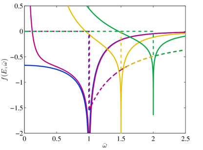
where , , and . For a vanishing gap, , the result approaches the graphene polarization function Kotov et al. (2012). One important difference is the fact that the imaginary part of the product , proportional to the low- conductivity, is not constant for . Instead, it has a maximum at which is the consequence of the high density of states at the extremal points of the bands. For undoped or ungated crystals, the chemical potential is located in the gap region, the conduction band is empty, and the conductivity becomes finite only for . As the system becomes n-doped, is nonzero at since interband transitions with smaller are forbidden. We plot the polarization function for several values of in Fig. 1. If the Fermi level is in the gap, the real part of polarization is always negative. This means that the dielectric function , where is the external dielectric constant, never changes sign and there are no collective charge excitations such as plasmons. Conversely, allowing electrons to populate the conduction band allows to pass through zero, giving rise to plasmonic behavior.
The screened Coulomb interaction between charge particles is given by the static polarization function. Since we are interested in excitons, we treat the case where the Fermi level is in the middle of the gap. Straightforward manipulations of Eq. (5) at yield:
| (7) | ||||
| (8) |
The asymptotic behavior of is given by:
| (9) |
The full system polarization is obtained by doubling Eq. (7) to account for the valley degeneracy and summing over to take care of both spins. Dividing the Coulomb term by the static gives the screened interaction potential. Taking the inverse Fourier transform of results in:
| (10) | ||||
| (11) |
where . For very small , we can use the large- approximation for in Eq. (10). This removes all -dependence from the denominator in (10) and results in a simple renormalization of the coupling constant which is identical to the static screening in undoped single layer graphene Kotov et al. (2012). In the opposite limit of large , there is no such renormalization and the Coulomb interaction remains unscreened.
To understand the nature of the screening, it is convenient to rewrie the polarization as
| (12) |
Next, we can obtain the charge induced by an external potential , with the Fourier transform . Using the simplest linear responce, one has . The second term in Eq. (12) yields
| (13) |
Integrating over in polar coordinates and multiplying by four to account for the degeneracy yields , located at the origin. This means that the external charge induces a screening charge located virtually at the same position. In fact, rewriting the screened energy at small as
| (14) |
shows that the screening arises from a number of induced charges with alternating signs located at the origin.
The first term in Eq. (12) has the sign opposite to the second term. It means that the charges induced from it are also opposite. Since the second term results in localized screening charges, those arising from the first term are compensating anti-screening. They are not localized and their effect becomes more pronounced at larger as the total sum enclosed in grows, eventually matching the screening one. A similar result was previously obtained for gapped graphene. Kotov et al. (2008) The authors showed that the anti-screening charge density has a logarithmic decay at smaller and drops off as at large distances. It was also demonstrated that most of the anti-screening charge is located at . Given that, according to Ref. Xiao et al., 2012, , the interaction becomes unscreened within a few lattice constants. Because of this, we will use the unscreened version, keeping in mind that the coupling constant may need to be adjusted from to include the screening at small enough distances.
IV Excitonic Collapse
Having established the nature of the Coulomb interaction in the system, we now turn our attention to the EQ. In order to keep the notation as simple as possible, we will dispense with the details of the SOC and simply denote the size of the gap by , keeping in mind that this quantity depends on the spin and the valley. It is convenient to perform a particle-hole transformation so that the electron and hole free Hamiltonians become:
| (15) |
Diagonalizing the Hamiltonian gives two branches with . Positive energies correspond to the states in the electron and hole bands while the negative ones represent the states in the electron and hole “seas”. The total Hamiltonian for two particles without interactions is given by the tensor product Sabio et al. (2010):
| (16) |
When dealing with excitons, one works in the center-of-mass frame of reference. Since in the model the masses of electrons and holes are the same, the momenta must be opposite. Setting results in four eigenvalues: and a doubly degenerate . The zero energy eigenstates arise from the cases when the system has a single electron or a hole and its complementary particle is in its sea. This way, since they have the same momentum, they give equal and opposite contributions to the total energy. The negative eigenvalue corresponds to the situation where both the electron and the hole are in their respective seas. Finally, the positive eigenvalue is what we are interested in. There, an electron is found in the electron band and the hole is the hole band. This can be regarded as an excitonic state with a vanishingly weak interaction. Therefore, the states of interest constitute a subspace of a full Hilbert space describing a two-particle system.
If we go back to the laboratory frame and investigate the kinetic energy of the exciton, and . Here, is the motion in the center of mass frame and is the momentum of the center of mass. Diagonalizing Eq. (16), one cannot separate the two momenta. However, assuming that , it is possible to estimate the kinetic energy as .
In principle, one can keep the masses of electrons and holes different. A particular case of interest is when one of these masses goes to infinity. In this case, the problem reduces to a particle moving in the field of a fixed charged impurity. Careful expansion of the two-particle eigenvalues gives for the excitonic energy, where is finite. The collapsing states of this system were treated in Ref. Pereira et al., 2008.
In the case of equal masses, the minimum energy of exciting an electron to the conduction band from the valence band is . We set up the bands in such a way that zero energy is located half-way between their extrema. This results in a reduced excitonic Hamiltonian:
| (17) |
where we have included the interaction term. Note that compared to the impurity problem Pereira et al. (2008), the momentum is doubled since the electron and hole are moving with the same momentum. We can perform a variable transformation , to preserve the commutation relation, yielding:
| (18) |
with . Notice that for the exciton problem the effective fine structure constant is half of the impurity case because of the doubling in the momentum. Equation (18) describes a massive Dirac particle in an attractive Coulomb potential of a single charge with coupling that is times stronger than the vacuum fine structure constant. The energies of the bound states are given by Pereira et al. (2008):
| (19) |
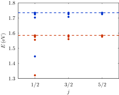
where is the principal quantum number and is the angular momentum quantum number. These determine the binding energies for the EQ and can be measured, say, by optical means. The optical absorption energies are given by the sum of and Eq. (19) since as , this sum approaches the size of the gap. Notice that for , some energies become imaginary. This is caused by the breakdown of the point-charge treatment of the center of the Coulomb well and is usually remedied by a regularization procedure, as we discuss below. For now, we avoid this problem by choosing to illustrate a particular case. As an example, we pick on a SiC substrate ( and )Xiao et al. (2012). Fig. 2 shows the absorption energies for this system. It is important to keep in mind that the exact system parameters depend strongly on experimental conditions. The nature of the substrate and the quality of the sample play a role. This means that these parameters need to be determined on a case-by-case basis.
For a regular Coulomb potential, the energies in Eq. (19) for the states are always positive. At sufficiently large , however, the energy “dives” to negative value until it eventually merges with the valence band at . To analyze this phenomenon, we need to introduce a regularization procedure to deal with the singularity of the Coulomb interaction. This entails imposing a potential cutoff at above which the interaction retains its usual form and for it becomes . The reason for choosing this particular length is that the physical lengths in the system are limited by the lattice spacing.
The form of the solution to Eq. (18) that we impose is:
| (20) |
Setting and solving Eq. (18) for yields Pereira et al. (2008):
| (21) | ||||
| (22) |
where , is a modified Bessel function, and is the normalization constant. Similarly, for , the result becomes Pereira et al. (2008):
| (23) | ||||
| (24) |
with . The solutions need to be matched at the boundary so that:
| (25) |
resulting in:
| (26) |
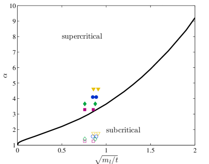
The cutoff point , while based on a physical quantity, might appear somewhat arbitrary. If one were to allow the cutoff to approach infinity, the critical coupling would approach the lowest root of . Therefore, the true value lies between these two limiting cases. In reality, one expects the cutoff to be closer to than to infinity.
The lowest energy levels, corresponding to , are the first to merge with the continuum. We determine the smallest values of that satisfy Eq. (26) for a given at and plot the result in Fig. 3. We also show where four STMDC’s are located in the phase diagram depending on the dielectric screening. Suspended samples with are all located in the supercritical regime. On the other hand, samples placed on BN with are located in the subcritical regime. Therefore, in order to possibly observe the excitonic collapse, for one needs to work substrates with .
V Conclusion
In conclusion, we have analyzed a long wavelength model for STMDC’s and obtained both the long-range and static polarization functions. We used the latter to determine the screening of Coulomb interactions in the system. This allowed us to solve for the energy levels of exciton quasiparticles. Most importantly, we obtained an equation which gives the critical coupling in a system that leads to a so-called excitonic collapse. Our results indicate that for strong enough coupling this phenomenon should be omnipresent in this class of materials.
We acknowledge DOE grant DE-FG02-08ER46512, ONR grant MURI N00014-09-1-1063, and the NRF-CRP award ”Novel 2D materials with tailored properties: beyond graphene” (R-144-000-295-281).
References
- Novoselov et al. (2004) K. S. Novoselov, A. K. Geim, S. V. Morozov, D. Jiang, Y. Zhang, S. V. Dubonos, I. V. Grigorieva, and A. A. Firsov, Science 306, 666 (2004).
- Novoselov et al. (2005) K. S. Novoselov, D. Jiang, F. Schedin, T. J. Booth, V. V. Khotkevich, S. V. Morozov, and A. K. Geim, Proc. Natl. Acad. Sci. USA 102, 10451 (2005).
- Castro Neto and Novoselov (2011) A. H. Castro Neto and K. Novoselov, Rep. Prog. Phys. 74, 082501 (2011).
- Wilson et al. (1975) J. A. Wilson, F. J. Di Salvo, and S. Mahajan, Adv. Phys. 24, 117 (1975).
- Wang et al. (2012) Q. H. Wang, K. Kalantar-Zadeh, A. Kis, J. N. Cole, and M. S. Strano, Nat. Nanotechnol. 7, 699 (2012).
- Chhowalla et al. (2013) M. Chhowalla, H. S. Shin, G. Eda, L.-J. Li, K. P. Loh, and H. Zhang, Nat. Chem. 5, 263 (2013).
- Fuhrer and Hone (2013) M. S. Fuhrer and J. Hone, Nat. Nanotech. 8, 146 (2013).
- Mak et al. (2010) K. F. Mak, C. Lee, J. Hone, J. Shan, and T. F. Heinz, Phys. Rev. Lett. 105, 136805 (2010).
- Xiao et al. (2012) D. Xiao, G.-B. Liu, W. Feng, X. Xu, and W. Yao, Phys. Rev. Lett. 108, 196802 (2012).
- Pereira et al. (2007) V. M. Pereira, J. Nilsson, and A. H. Castro Neto, Phys. Rev. Lett. 99, 166802 (2007).
- Shytov et al. (2007) A. V. Shytov, M. I. Katsnelson, and L. S. Levitov, Phys. Rev. Lett. 99, 246802 (2007).
- Wang et al. (2013) Y. Wang, D. Wong, A. V. Shytov, V. W. Brar, S. Choi, Q. Wu, H.-Z. Tsai, W. Regan, A. Zettl, R. K. Kawakami, S. G. Louie, L. S. Levitov, and M. F. Crommie, Science 340, 734 (2013).
- Kane and Mele (2005a) C. L. Kane and E. J. Mele, Phys. Rev. Lett. 95, 226801 (2005a).
- Kane and Mele (2005b) C. L. Kane and E. J. Mele, Phys. Rev. Lett. 95, 146802 (2005b).
- Rostami et al. (2013) H. Rostami, A. G. Moghaddam, and R. Asgari, Phys. Rev. B 88, 085440 (2013).
- Kotov et al. (2012) V. N. Kotov, B. Uchoa, V. M. Pereira, F. Guinea, and A. H. Castro Neto, Rev. Mod. Phys. 84, 1067 (2012).
- Kotov et al. (2008) V. N. Kotov, V. M. Pereira, and B. Uchoa, Phys. Rev. B 78, 075433 (2008).
- Sabio et al. (2010) J. Sabio, F. Sols, and F. Guinea, Phys. Rev. B 81, 045428 (2010).
- Pereira et al. (2008) V. M. Pereira, V. N. Kotov, and A. H. Castro Neto, Phys. Rev. B 78, 085101 (2008).