Integration and characterization of solid wall electrodes in microfluidic devices fabricated in a single photolithography step
Abstract
We describe the fabrication and characterization of solid 3-dimensional electrodes in direct contact with microfluidic channels, implemented using a single photolithography step, allowing operation in high-dielectric constant media. Incorporation and self-alignment of electrodes is achieved by combining microsolidic approaches with exploitation of the surface tension of low melting point alloys. Thus the metal forms the walls flanking the channel. We show that this approach yields electrodes with a well-defined, reproducible morphology and stable electronic properties when in contact with biochemical buffers. By combining calibration of the electric field with free-flow electrophoresis we quantify the net solvated charges of small molecules.
pacs:
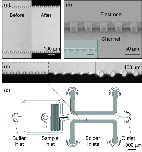
82.45.Tv, 84.37.+q, 87.15.-v, 87.15.TtThe ability to control electric fields within microfluidic devices is the foundation for many key applications of this technologyVoldman et al. (2002); Burg and Manalis (2003); Ahn et al. (2006); Burg et al. (2007); Kohlheyer et al. (2008); He and Herr (2009); Abate et al. (2010); Agresti et al. (2010); Mojarad and Krishnan (2012); O’Donovan et al. (2012); Song et al. (2013). Approaches exist to use microsolidics techniquesSiegel et al. (2007) in combination with soft lithography to generate electrodes within separate channels that are suitable for use in low-dielectric media such as oils utilized in digital microfluidicsAbate et al. (2010); however, strong electrostatic screening in conductive aqueous media from ionic species present in solution necessitates the use of fundamentally different approaches to generate strong fields in such media. Indeed, direct electric contact between the electrodes and the conductive sample media, such as aqueous buffer solutions, is required to prevent screening at the electrode interface. This requirement presents a challenge for micro-fabrication, and conventional methods for the integration of such elements rely on multistep processes and controlled alignment of such elements to ensure the accurate relative positioning of the fluidic and electronic components of the deviceKohlheyer et al. (2006); Kim et al. (2007); Ebina et al. (2009); Romanowsky et al. (2010); Köhler et al. (2011); Cheng et al. (2011). In this Letter, we combine microsolidics techniques with exploitation of the surface tension of molten InBiSn alloy to fabricate 3-dimensional (3D) electrodes in direct contact with aqueous media within microfluidic devicesSo and Dickey (2011); Li et al. (2012). We characterize the electronic properties of the devices and show that this approach allows a stable electrode/solvent interface to be positioned with micrometer precision as shown in Fig. 1(a) to (c). Furthermore, we demonstrate the use of such electrodes in free-flow micro-electrophoresis to determine accurately the charges of molecular species in solution.

In order to create a direct contact between the metal electrodes and electrolyte within microfluidic channels, we generated, using soft-lithography, arrays of pillars to define the position of the electrodes within the channelsSo and Dickey (2011). The corresponding sections at the sides of the channel were subsequently filled with a molten InBiSn alloy which was allowed to solidify within the device. Resulting in a large active area and a vertically homogeneous electric field. This is in contrast to conventional approaches where the electrodes are patterned onto the basis of the microchannels.
The microchannels were fabricated in polydimethylsiloxane (PDMS) on glass substrates using standard soft lithography techniquesMcDonald and Whitesides (2002). In order to minimize experimental noise, opaque devices were produced by mixing a small fraction of carbon nano powder, 0.2 % w/w, into the PDMS prior to curing. Electrodes, see Fig. 1(a) and (c), were incorporated by inserting a low melting point InBiSn alloy (51% In, 32.5% Bi, 16.5% Sn, Conro Electronics) through the designated channels of devices placed, glass slide down, on a hot plate set to . At this temperature, the alloy melts upon contact with the glass substrate and fills the designated channels upon light pressure, but is sufficiently viscous and possesses a sufficient surface tension so as not to flow between the pillars. The inserted electrodes then solidify at room temperature. The fabrication process therefore enables the production of microfluidic devices incorporating 3D electrodes automatically aligned with fluidic components and in direct contact with them.
This approach allows pillar arrays with a range of dimensions to be used in conjunction with the surface tension of molten solder to integrate electrodes in microfluidic devices, as demonstrated in Fig. 1(c). An upper limit to pillar size and spacing is given by the requirement to prevent the flow of the molten metal between the pillars; in practise effective containment is lost for spacings exceeding 75 m. The practical lower limit to pillar sizing is given by the soft lithography process used to define themMcDonald and Whitesides (2002) In the remainder of this Letter, we work with a pillar diameter and spacing of 25 m in each case.

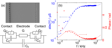
We characterized the stability of the electronic properties of the 3D electrodes in solution and their suitability for applying controlled electric fields in aqueous media within microfluidic devices by repeatedly measuring the frequency-dependent admittance of the device shown in Fig. 1(c) and comparing the results with a suitable circuit model. A scheme of an equivalent circuit for the device is presented in Fig. 2(a), where the fluid channel is modeled as a conductance in series between two solder-to-fluid contacts, characterized by a (low) conductance and a parallel capacitance , with an overall stray capacitance . To perform the calibration measurement, a AC voltage with variable frequency was applied over a device filled with a conductivity standard. The resulting current, and thus the admittance , was then measured as a voltage drop over a resistor using a lock-in amplifier and is shown in Fig. 2(b).
At very low frequencies, the overall conductance is limited by the low conductance of the contacts. At intermediate frequencies of approximately , the conductance through the contact capacitance exceeds the one through the contact resistance, leading to a linear increase of the admittance with the frequency. Above , the conductance of the channel itself becomes the limiting factor governing the overall current flow, and the absolute value of the admittance is constant with frequency until conductance through the stray capacitance becomes appreciable. Comparison to the modeled, complex frequency-dependent admittance (dashed lines in Fig. 2(b) allows for determination of the circuit parameters introduced above, and we obtain contact capacitances of the order of a few nF, stray capacitances in the range of a few pF and contact resistances much larger than . Moreover, using the given conductivity of the standard solution thus allows us also to determine the cell constant linking conductance and conductivity in each device.
Our model fits the experimental data very well, with noticeable deviations only at very low frequencies where conductance is low. Furthermore, since the value of is directly given by the constant part of the spectrum and is independent of the values of the other fit parameters. The values we obtain for the individual cell constants are highly reliable and reproducible between devices. The mean cell constant and standard deviation for 10 devices were found to be . These results also agree well with calculated valuesnot (a), but variation outside the overlap of error bounds were observed when investigating different devices in spite of the shared lithographic dimensions, highlighting the advantage of the direct experimental calibration afforded by this setup.
The functionality of these well-characterized electrodes can be explored by performing quantitative free-flow micro electrophoresis. A key requirement for charge quantification of molecular species by electrophoresis in free solution is the ability to determine accurately both the flow profile and the electric field strength across the solution where sample deflection occurs. In order to quantify the electric field inside the flow channel accurately, we use the calibrated cell constants for the individual devices and measure the conductivities of each of the buffers used. Recording of the DC current flowing through a given device upon application of a voltage then permits the effective voltage drop over the liquid to be determined via , which in turn yields the electric field through , with the effective width of the channelnot (b).
To study the electrophoretic mobility of analytes under controlled conditions of pH and ionic strength, simultaneous electric current and analyte deflection measurements were undertaken for a range of voltages in three common biochemical buffer systems. Measurements were made in HEPES, Tris and phosphate buffers, each at concentrations of 2.5, 5 and 10 mM, and all at pH 8.0. The fluorescent dyes fluorescein and rhodamine 6G were chosen as a model analytes.

Experiments were performed at a flow rate of . The flow velocity in the central wide section of the channel, averaged in the vertical direction, is to a good approximation constant with lateral position across the channel due to the high aspect ratio. We evaluated the average flow velocity in this areato be , resulting in a mean residence time between the electrodes of .
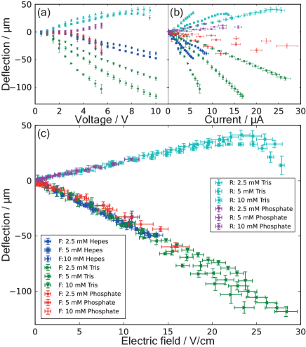
The position of the fluorescence intensity maximum of a flow-focused fluorescein or rhodamine beam in different buffer solutions upon application of a DC voltage to the electrodes is shown in Fig. 3(a). Data were recorded using a CCD camera operating through long working distance inverted optics with an integration time of and averaged over 25 pixels corresponding to along the flow direction, with four repeats.
Sample deflection of the order of tens of was observed in all buffer systems investigated. However the observed voltage threshold below which ionic screening at the electrode-liquid interface inhibits the current between them, and thereby analyte deflection, varies between the three buffers. Furthermore the voltage drop across the solution relative to that at the metal-liquid interface varies with buffer concentration, affecting the extent of analyte deflection. These observations emphasize that the electric field in the solution is not simply proportional to the overall voltage drop, and highlights the requirement for simultaneous current measurements to calculate the electric field strength from the effective voltage drop over the solution.
When moving close to the electrodes, reaction of the dyes with electrolysis products may result in loss of fluorescence, as seen from the apparent decrease in the deflection data for rhodamine 6G in 5 and 10 mM Tris at higher applied voltages in Fig. 3. This observation does not affect the dye at locations further from the electrodes, defining the dynamic operating range of the setup.
A near-linear dependence of analyte deflection on current is observed when the same deflection data is plotted against the simultaneously measured current in Fig. 3(b). However, due to the differences in buffer conductivities a range of deflections are seen for equal currents. We note that at these low voltages and currents the nucleation and bubble formation of electrolysis productsKohlheyer et al. (2006); Kim et al. (2007); Köhler et al. (2011) is avoided.

Remarkably, when the deflection is plotted as a function of calibrated electric field in Fig. 3(c), the data collapse accurately into an almost linear relationship, the slope of which defines the electrophoretic mobility . To avoid perturbation of by ion depletion due to the low flow velocities at channel edges or reaction with electrolysis products, linear fits were performed to data for field strengths below . In this manner, the electrophoretic mobility of the molecular species is found from division of the mean of these slopes by the residence time in the channel () to give electrophoretic mobilities of for fluorescein and in the case of rhodamine 6G. The main contribution to the error on the residence time is the height of the channel . All devices used in the experiments presented here were fabricated using the same lithography master, hence variation is not expected between devices.
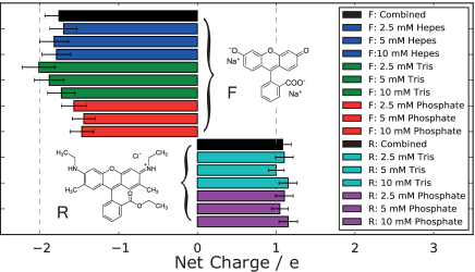
The measured electrophoretic mobilities can be converted to the corresponding solvated charge for molecules of known radii, here we used for the radius of fluoresceinMontermini et al. (2002) and for rhodamine 6GMüller et al. (2008). These values correspond to solvated charges of for fluorescein and for rhodamine 6G, see black bars in Fig. 4. These charges determined under solution conditions are in good agreement with those anticipated from the dissociation of the dyes and counter ions shown in the insets of Fig. 4.
In conclusion, an adaptable design and fabrication method for the incorporation of solid 3D electrodes of complex geometries into microfluidic devices is presented. A single photolithography step is required in the fabrication of inherently aligned solid electrodes in direct contact with sample solutions. Free-flow electrophoresis was performed in a voltage range where electrolysis products are carried away by the liquid flow through the device. Three buffer systems were characterized at low mM concentrations. Simultaneous measurements were made of both analyte deflection and current at the application of increasing voltages. The cell constants of the devices were calibrated using conductivity standards. Conductivity measurements of the individual buffer solutions were used to quantify the electric field strength within the electrolyte, enabling the determination of the electrophoretic mobility and the charge of molecules in solution.
Support from the Biotechnology and Biological Sciences Research Council (BBSRC), the Frances and Augustus Newman Foundation, the Engineering and Physical Sciences Research Council (EPSRC) and the Swiss National Science Foundation (SNF) is gratefully acknowledged.
References
- Voldman et al. (2002) J. Voldman, M. L. Gray, M. Toner, and M. A. Schmidt, Analytical C hemistry 74, 3984 (2002).
- Burg and Manalis (2003) T. P. Burg and S. R. Manalis, Applied Physics Letters 83, 2698 (2003).
- Ahn et al. (2006) K. Ahn, C. Kerbage, T. P. Hunt, R. Westervelt, D. R. Link, and D. Weitz, Applied Physics Letters 88, 024104 (2006).
- Burg et al. (2007) T. P. Burg, M. Godin, S. M. Knudsen, W. Shen, G. Carlson, J. S. Foster, K. Babcock, and S. R. Manalis, Nature 446, 1066 (2007).
- Kohlheyer et al. (2008) D. Kohlheyer, J. Eijkel, A. van den Berg, and R. Schasfoort, Electrophoresis 29, 977 (2008).
- He and Herr (2009) M. He and A. Herr, Analytical Chemistry 81, 8177 (2009).
- Abate et al. (2010) A. Abate, T. Hung, P. Mary, J. Agresti, and D. Weitz, Proceedings of the National Academy of Sciences 107, 19163 (2010).
- Agresti et al. (2010) J. Agresti, E. Antipov, A. Abate, K. Ahn, A. Rowat, J. Baret, M. Marquez, A. Klibanov, A. Griffiths, and D. Weitz, Proceedings of the National Academy of Sciences 107, 4004 (2010).
- Mojarad and Krishnan (2012) N. Mojarad and M. Krishnan, Nature Nanotechnology 7, 448 (2012).
- O’Donovan et al. (2012) B. O’Donovan, D. Eastburn, and A. Abate, Lab on a Chip (2012).
- Song et al. (2013) Y. Song, Z. Liu, T. Kong, and H. Shum, Chemical Communications (2013).
- Siegel et al. (2007) A. Siegel, D. Bruzewicz, D. Weibel, and G. Whitesides, Advanced Materials 19, 727 (2007).
- Kohlheyer et al. (2006) D. Kohlheyer, G. A. J. Besselink, S. Schlautmann, and R. B. M. Schasfoort, Lab on a Chip 6, 374 (2006).
- Kim et al. (2007) S. Kim, J. Kim, K. Kim, and T. Chung, Analytical Chemistry 79, 7761 (2007).
- Ebina et al. (2009) W. Ebina, A. Rowat, and D. Weitz, Biomicrofluidics 3,(2009).
- Romanowsky et al. (2010) M. B. Romanowsky, M. Heymann, A. R. Abate, A. T. Krummel, S. Fraden, and D. A. Weitz, Lab on a Chip 10, 1521 (2010).
- Köhler et al. (2011) S. Köhler, C. Weilbeer, S. Howitz, H. Becker, V. Beushausen, and D. Belder, Lab on a Chip 11, 309 (2011).
- Cheng et al. (2011) Y. Cheng, X. Luo, C. Tsao, H. Wu, J. Betz, G. Payne, W. Bentley, and G. Rubloff, Lab on a Chip 11, 2316 (2011).
- So and Dickey (2011) J.-H. So and M. D. Dickey, Lab on a Chip 11, 905 (2011).
- Li et al. (2012) S. Li, M. Li, Y. Hui, W. Cao, W. Li, and W. Wen, Microfluidics and Nanofluidics, 1 (2012).
- McDonald and Whitesides (2002) J. McDonald and G. Whitesides, Accounts of Chemical Research 35, 491 (2002).
- not (a) The calculation was performed by numerically iterating the Poisson equation with the potentials of rectangular electrodes apart as boundary conditions and comparing the applied voltage to the resulting electric field evaluated across the entire length of the device (extending well beyond the end of the electrodes).
- not (b) The measured width between the faces of the electrodes was . To account for the decreased channel area between the pillars their diameter of was counted twice and a generous error estimate of attributed to the conversion from effective voltage drop to electric field.
- Spiga M (1994) M. G. Spiga M, International Communications in Heat and Mass Transfer 21, 469 (1994).
- Montermini et al. (2002) D. Montermini, C. Winlove, and C. Michel, The Journal of Physiology 543, 959 (2002).
- Müller et al. (2008) C. Müller, A. Loman, V. Pacheco, F. Koberling, D. Willbold, W. Richtering, and J. Enderlein, Europhysics Letters 83, 46001 (2008).